STM32F767BIT6 vs STM32F767NIH6 Vergleich
Detaillierter Direktvergleich von STM32F767BIT6 von STMicroelectronics und STM32F767NIH6 von STMicroelectronics. Vergleichen Sie die wichtigsten Spezifikationen, elektrischen Parameter, Gehäuse, Lebenszyklusstatus, Preise und Verfügbarkeit, um das beste Bauteil für Ihre Designanforderungen zu ermitteln.
STMicroelectronics

STM32F767BIT6 - ARM Cortex-M7 MCU, 2MB Flash, 216MHz | STMicroelectronics
STM32F767BIT6 ✓ AktivSTMicroelectronics
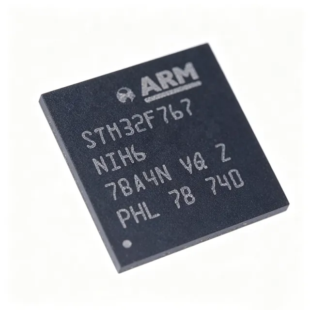
STM32F767NIH6 - 32-bit ARM Cortex-M7 MCU, 2MB Flash, 216MHz | STMicroelectronics
STM32F767NIH6 ✓ AktivSpezifikationsvergleich
| Parameter | STM32F767BIT6 | STM32F767NIH6 |
|---|---|---|
| Marke | STMicroelectronics | STMicroelectronics |
| Kategorie | Microcontrollers | Microcontrollers |
| Lebenszyklusstatus | Aktiv | Aktiv |
| Lagerstatus | In Stock | In Stock |
| Stückpreis (USD) | $11,85 | $10,85 |
| Core | ARM Cortex-M7 with FPU + DSP instructions | Arm 32-bit Cortex-M7 with double-precision FPU |
| Maximum CPU Clock | 216 MHz | — |
| DMIPS | 462 DMIPS (2.14 DMIPS/MHz, Dhrystone 2.1) | — |
| Program Flash | 2 MB (single-bank, 32-bit fetch) | — |
| SRAM | 384 KB DTCM + 128 KB SRAM + 4 KB backup SRAM | — |
| L1 Cache | 16 KB I-cache + 16 KB D-cache | — |
| ART Accelerator | Yes (0-wait-state execution from Flash) | — |
| Operating Voltage | 1.7 V to 3.6 V | — |
| Gehäuse | 208-LQFP (28x28 mm), 0.5 mm pitch | TFBGA-216 (13x13mm, 0.8mm pitch) |
| I/O Pins (max) | 162 GPIOs | — |
| ADC | 3 x 12-bit, up to 2.4 MSPS each | 16-bit, up to 3.6 MSPS |
| DAC | 2 x 12-bit | 12-bit |
| Timers | up to 18 channels incl. 32-bit, IC/OC, PWM | — |
| USB | USB 2.0 OTG FS + HS with integrated HS PHY | — |
| CAN | 2 x CAN 2.0B | — |
| Crypto / Hash | AES-256, SHA-1/2, TRNG (hardware) | — |
| External Memory Bus | SDRAM (up to 32-bit) + SRAM/PSRAM/NOR/NAND | — |
| Display Controller | LCD-TFT, up to 1024x768 + DMA2D | — |
| Octo-SPI / Quad-SPI | 1 x Octo-SPI / 1 x Quad-SPI | — |
| Betriebstemperatur | -40°C to +85°C (Grade 6) | — |
| Montageart | Surface Mount | — |
| MSL-Level | 3 (per JEDEC J-STD-020) | — |
| RoHS-Status | Compliant | Compliant |
| Maximale Taktfrequenz | — | 216 MHz |
| CoreMark / DMIPS | — | 462 DMIPS / 2.14 DMIPS/MHz (Dhrystone 2.1) |
| Cache | — | 16 Kbytes I/D L1-cache |
| Program Memory Size | — | 2 MB Flash (dual-bank) |
| RAM Memory Size | — | 512 KB SRAM |
| Operating Voltage Range | — | 1.7 V to 3.6 V |
| Betriebstemperaturbereich | — | -40 C to +85 C (industrial grade) |
| Number of I/O Lines | — | 159 |
| External Data Bus | — | 32-bit |
| External Address Bus | — | 26-bit |
| I2C Interfaces | — | 4 |
| UART / USART | — | 4 USART + 4 UART |
| SPI Interfaces | — | 6 |
| CAN Interfaces | — | 3 |
| USB Interfaces | — | 2x USB OTG |
| Ethernet | — | 1x 10/100 MAC |
| SDMMC | — | 1x |
| Cryptography | — | AES, DES, 3DES, TRNG |
| Graphics | — | Chrom-ART Accelerator, TFT LCD controller, JPEG codec |
| DSP | — | Yes (DSP instructions) |