XC7A100T-1CSG324C vs XC7A100T Comparison
Detailed side-by-side comparison of XC7A100T-1CSG324C by AMD and XC7A100T by AMD. Compare key specifications, electrical parameters, packaging, lifecycle status, pricing, and availability to determine the best component for your design requirements.
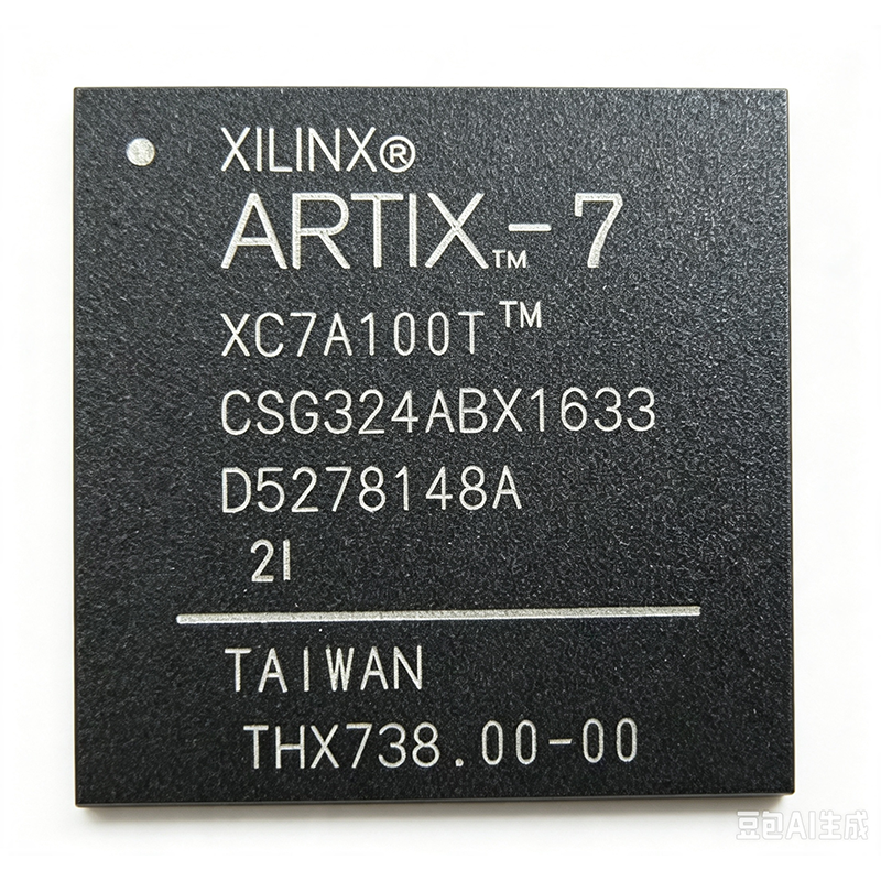

Specification Comparison
| Parameter | XC7A100T-1CSG324C | XC7A100T |
|---|---|---|
| Brand | AMD | AMD |
| Category | FPGA & CPLD | FPGA & CPLD |
| Lifecycle Status | Active | Active |
| Stock Status | In Stock | In Stock |
| Unit Price (USD) | $59.90 | $27.90 |
| Family | Artix-7 | Artix-7 |
| Logic Cells | 101,440 | 101440 |
| System Logic Cells (equivalent) | 285,000 | — |
| Block RAM | 4,860 Kb | 4860 Kb |
| DSP Slices | 240 | — |
| User I/O Pins | 210 | — |
| Package | CSG324 (324-ball Chip Scale BGA) | — |
| Speed Grade | -1 | — |
| Core Voltage (VCCINT) | 1.0 V | — |
| I/O Voltage (VCCO) | 1.2 V to 3.3 V | — |
| GTP Transceivers | 8 (up to 6.6 Gbps) | — |
| PCIe Blocks | 1 (Gen2 x4) | — |
| XADC | 1 (12-bit, 1 MSPS) | — |
| Operating Temperature | 0C to +85C (Commercial) | — |
| RoHS Status | Compliant | — |
| Slices | — | 15850 |
| DSP48E1 Slices | — | 240 |
| Clock Management Tiles (CMT) | — | 6 |
| Maximum User I/O (CSG324) | — | 210 |
| Process Technology | — | 28 nm |
| Speed Grades | — | -1, -2, -3 |
| Temperature Ranges | — | C: 0C to +85C, I: -40C to +100C |
| Packages | — | CSG324, FTG256, FGG484, FGG676 |
| I/O Standards | — | LVCMOS, LVDS, HSTL, SSTL |
| Bank I/O Voltage | — | 1.2 V to 3.3 V |
| Integrated Hard IP | — | PCIe, XADC (12-bit), DDR3 memory controller support |
| Transceiver Line Rate | — | Up to 6.6 Gbps (GTP, select packages) |
| Design Software | — | AMD Vivado Design Suite |
| Reference Datasheet | — | DS181 Artix-7 DC and AC Switching Characteristics |