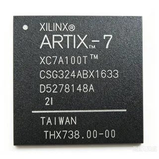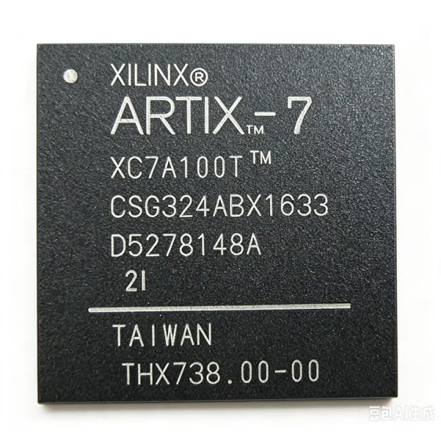
XC7A100T-1CSG324C - Artix-7 FPGA, 101K Logic Cells | AMD Xilinx
MPN: XC7A100T-1CSG324C ✓ Active| Qty | Unit Price | Extended |
|---|---|---|
| 1 | $89.5 | $89.50 |
| 10 | $82.3 | $823.00 |
| 100 | $74.1 | $7,410.00 |
| 500 | $66.8 | $33,400.00 |
| 1,000 | $59.9 | $59,900.00 |
XC7A100T-1CSG324C Overview
An FPGA (Field-Programmable Gate Array) is an integrated circuit that can be configured by the designer after manufacturing, allowing for custom digital logic implementations. FPGAs sit within the broader category of programmable logic devices (PLDs), which are part of the semiconductor industry. They offer a balance between the flexibility of software and the performance of fixed-function ASICs, enabling rapid prototyping and hardware acceleration.
Key features include 285,000 system logic cells (equivalent), 240 DSP48E1 slices for digital signal processing, and 4,860 Kb of fast block RAM. The device supports a wide range of I/O standards including LVCMOS, LVDS, and HSTL, with up to 210 user I/O pins in the CSG324 package. The -1 speed grade provides a balance of performance and power, with a maximum clock frequency of approximately 400 MHz for internal logic.
The Artix-7 architecture is built on a 28nm high-k metal gate (HKMG) process, offering low static power consumption and high logic density. The device includes integrated PCIe Gen2 blocks, XADC for analog-to-digital conversion, and GTP transceivers (up to 6.6 Gbps) for high-speed serial communication. These features make it a versatile choice for a wide range of applications.
Typical applications include software-defined radio, motor control, industrial networking, and video processing. The XC7A100T-1CSG324C is particularly well-suited for applications requiring high I/O count and moderate logic resources, such as interface bridging and protocol conversion.
When designing with this FPGA, careful attention must be paid to power supply decoupling and thermal management. The device requires multiple supply rails (VCCINT, VCCAUX, VCCO) and a proper power-up sequence. Use the Xilinx Power Estimator (XPE) to calculate power consumption and design an appropriate thermal solution.
This page synthesizes distributor pricing, drop-in alternatives, and practical design notes not found in the AMD Xilinx datasheet, providing a comprehensive resource for engineers evaluating the XC7A100T-1CSG324C.
Drop-in alternatives for XC7A100T-1CSG324C — same package, pin-to-pin compatible. Different-package parts requiring PCB rework are excluded.
Variants in this series
Same-series models that are drop-in compatible with XC7A100T-1CSG324C (same form factor and footprint) — differing in Block RAM, Logic Cells, Package, Speed Grade, DSP Slices.
Quick Comparison Tool — Select alternative parts for side-by-side comparison:
XC7A100T-2CSG324C
✓ In Stock
$59.5 / Unit
View Datasheet →XC7A100T-1CSG324I
✓ In Stock
$59.9 / Unit
View Datasheet →XC7A100T-2CSG324I
✓ In Stock
$105 / Unit
View Datasheet →XC7A100T-1CSG324C Maximum Ratings & Electrical Characteristics
| Family | Artix-7 |
| Logic Cells | 101,440 |
| System Logic Cells (equivalent) | 285,000 |
| Block RAM | 4,860 Kb |
| DSP Slices | 240 |
| User I/O Pins | 210 |
| Package | CSG324 (324-ball Chip Scale BGA) |
| Speed Grade | -1 |
| Core Voltage (VCCINT) | 1.0 V |
| I/O Voltage (VCCO) | 1.2 V to 3.3 V |
| GTP Transceivers | 8 (up to 6.6 Gbps) |
| PCIe Blocks | 1 (Gen2 x4) |
| XADC | 1 (12-bit, 1 MSPS) |
| Operating Temperature | 0C to +85C (Commercial) |
| RoHS Status | Compliant |
XC7A100T-1CSG324C Pin Configuration
| Pin A1 | IO_L1N_T0 — User I/O (LVDS pair negative) |
| Pin A2 | IO_L1P_T0 — User I/O (LVDS pair positive) |
| Pin B1 | GND — Ground |
| Pin B2 | VCCINT — Core voltage 1.0V |
| Pin C1 | IO_L2N_T0 — User I/O |
| Pin C2 | IO_L2P_T0 — User I/O |
| Pin D1 | VCCAUX — Auxiliary voltage 1.8V |
| Pin D2 | GND — Ground |
| Pin E1 | IO_L3N_T0 — User I/O |
| Pin E2 | IO_L3P_T0 — User I/O |
| Pin F1 | VCCO_0 — I/O bank 0 supply voltage |
| Pin F2 | GND — Ground |
Typical Applications
XC7A100T-1CSG324C is suitable for 6 applications: Software-Defined Radio, Motor Control, Industrial Networking, Video Processing, Test and Measurement, Aerospace and Defense.
Software-Defined Radio
The XC7A100T-1CSG324C is ideal for software-defined radio (SDR) systems due to its 240 DSP slices and 8 GTP transceivers. In an SDR, the FPGA performs digital down/up conversion, filtering, and modulation/demodulation. The DSP slices handle high-speed multiply-accumulate operations for FIR filters and FFTs, while the GTP transceivers interface with high-speed ADCs/DACs and Ethernet backhaul. The 4,860 Kb of block RAM provides buffering for continuous data streams. With a -1 speed grade, the device can sustain sample rates up to 100 MSPS for wideband signals. Designers can implement a complete SDR signal chain in a single FPGA, reducing component count and latency. Power consumption is manageable with proper clock gating and resource utilization, making it suitable for portable and fixed SDR platforms.
Recommended
Motor Control
The XC7A100T-1CSG324C is well-suited for advanced motor control applications, such as servo drives and robotics. Its 240 DSP slices enable high-speed PID loops and space-vector modulation (SVM) algorithms. The FPGA can generate PWM signals with precise timing, and its 210 user I/O pins allow direct connection to encoder interfaces and current sensors. The -1 speed grade provides sufficient performance for control loop rates up to 20 kHz. The device's low static power and commercial temperature range make it cost-effective for industrial drives. Designers can implement safety features like overcurrent protection and fault handling in hardware, ensuring deterministic response. The GTP transceivers can be used for real-time communication with higher-level controllers via EtherCAT or PROFINET.
Recommended
Industrial Networking
The XC7A100T-1CSG324C is an excellent choice for industrial networking equipment, such as managed Ethernet switches and protocol converters. Its 8 GTP transceivers support multiple Gigabit Ethernet ports, and the integrated PCIe block enables host processor interfaces. The FPGA can implement Layer 2 switching, VLAN tagging, and QoS in hardware, achieving wire-speed performance. The 4,860 Kb of block RAM is sufficient for packet buffering and forwarding tables. The -1 speed grade is adequate for 1Gbps line rates, and the commercial temperature range covers typical industrial environments. The device's high I/O count allows connection to PHY chips and management interfaces. Designers can also implement custom protocols like PROFINET or EtherCAT for real-time control networks.
Recommended
Video Processing
The XC7A100T-1CSG324C is suitable for video processing applications, including image scaling, color space conversion, and frame buffering. Its 240 DSP slices can implement filters and transforms, while the 4,860 Kb of block RAM supports line buffers and frame storage. The device supports various video standards via its I/O pins, including LVDS and TMDS for HDMI. The -1 speed grade can handle 1080p60 video streams with moderate processing. The GTP transceivers can be used for SDI (Serial Digital Interface) video transport. Designers can implement custom video pipelines with low latency, making it ideal for broadcast and medical imaging. The commercial temperature range is suitable for consumer and professional equipment.
Recommended
Test and Measurement
The XC7A100T-1CSG324C is well-suited for test and measurement instruments, such as logic analyzers, signal generators, and data acquisition systems. Its high I/O count and GTP transceivers enable high-speed data capture and generation. The XADC block provides on-chip analog-to-digital conversion for monitoring voltages and temperatures. The DSP slices can implement digital signal processing for waveform analysis. The -1 speed grade is sufficient for sample rates up to 1 GSPS using deserialization techniques. The device's flexibility allows designers to create custom triggering and measurement logic. The commercial temperature range is adequate for benchtop instruments. Designers can also implement USB or Ethernet interfaces using the GTP transceivers for remote control.
Recommended
Aerospace and Defense
The XC7A100T-1CSG324C is used in aerospace and defense applications, including radar processing, secure communications, and electronic warfare. Its DSP slices and block RAM enable real-time signal processing, while the GTP transceivers support high-speed data links. The device's commercial temperature range limits it to ground-based or controlled environments; for harsh environments, consider the industrial (-I) variant. The FPGA's reprogrammability allows for field upgrades and adaptive algorithms. The -1 speed grade provides a balance of performance and power for battery-powered systems. Designers can implement encryption and anti-tamper features in hardware. The device is also used in UAV payloads for video and sensor processing.
Recommended
Recommended Products Summary
Engineering reference data for XC7A100T-1CSG324C — comparison, design guidance, and compliance information.
Selection Guide
Comparison with Alternatives
| Parameter | This Product | XC7A100T-2CSG324C | XC7A100T-1CSG324I | XC7A100T-2CSG324I |
|---|---|---|---|---|
| Package | CSG324 | CSG324 - same | CSG324 - same | CSG324 - same |
| Speed Grade | -1 | -2 | -1 | -2 |
| Temperature Range | 0C to +85C | 0C to +85C | -40C to +100C | -40C to +100C |
| Logic Cells | 101,440 | 101,440 | 101,440 | 101,440 |
| Block RAM | 4,860 Kb | 4,860 Kb | 4,860 Kb | 4,860 Kb |
| DSP Slices | 240 | 240 | 240 | 240 |
| User I/O Pins | 210 | 210 | 210 | 210 |
| GTP Transceivers | 8 | 8 | 8 | 8 |
Key Differentiators
- Lower cost and power consumption (vs XC7A100T-2CSG324C)
- Commercial temperature range (vs XC7A100T-1CSG324I)
- Balanced performance and I/O count (vs XC7A100T-1FTG256C)
Design Notes
The XC7A100T-1CSG324C requires multiple power rails: VCCINT at 1.0V, VCCAUX at 1.8V, and VCCO for each I/O bank (1.2V to 3.3V). Use low-dropout regulators or DC-DC converters with proper decoupling. Place 100nF capacitors near each power pin and bulk capacitors (10uF) on the board. Follow the power-up sequence: VCCINT, then VCCAUX, then VCCO to avoid latch-up.
The CSG324 package has a thermal resistance (theta_JA) of approximately 20C/W without airflow. For typical designs consuming 2-3W, the junction temperature rise is 40-60C above ambient. Ensure adequate airflow or a heatsink for high-utilization designs. Use the Xilinx Power Estimator (XPE) to calculate power and verify thermal margins.
For the CSG324 BGA package, use a 4-layer or more PCB with dedicated power and ground planes. Route high-speed GTP transceiver signals with controlled impedance (100 ohm differential). Place decoupling capacitors as close as possible to the FPGA power pins. Follow AMD Xilinx PCB design guidelines for BGA escape routing and via placement.
Compliance Information
RoHS compliant per AMD Xilinx environmental data. Not AEC-Q100 qualified as it is not an automotive-grade device.