XC7A100T-1CSG324C vs XC7A100T-1FTG256C Comparison
Detailed side-by-side comparison of XC7A100T-1CSG324C by AMD and XC7A100T-1FTG256C by AMD. Compare key specifications, electrical parameters, packaging, lifecycle status, pricing, and availability to determine the best component for your design requirements.
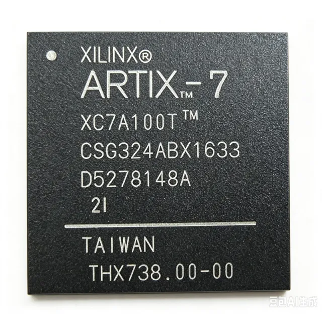

Specification Comparison
| Parameter | XC7A100T-1CSG324C | XC7A100T-1FTG256C |
|---|---|---|
| Brand | AMD | AMD |
| Category | FPGA & CPLD | FPGA & CPLD |
| Lifecycle Status | Active | Active |
| Stock Status | In Stock | In Stock |
| Unit Price (USD) | $59.90 | $215.00 |
| Family | Artix-7 | Artix-7 |
| Logic Cells | 101,440 | 101,440 |
| System Logic Cells (equivalent) | 285,000 | — |
| Block RAM | 4,860 Kb | — |
| DSP Slices | 240 | — |
| User I/O Pins | 210 | — |
| Package | CSG324 (324-ball Chip Scale BGA) | 256-ball FTBGA (FTG256) |
| Speed Grade | -1 | -1 |
| Core Voltage (VCCINT) | 1.0 V | — |
| I/O Voltage (VCCO) | 1.2 V to 3.3 V | — |
| GTP Transceivers | 8 (up to 6.6 Gbps) | — |
| PCIe Blocks | 1 (Gen2 x4) | — |
| XADC | 1 (12-bit, 1 MSPS) | — |
| Operating Temperature | 0C to +85C (Commercial) | — |
| RoHS Status | Compliant | Compliant |
| Block RAM (bits) | — | 4,976,640 |
| Block RAM (Kb) | — | 4,860 |
| DSP Slices (DSP48E1) | — | 240 |
| Temperature Grade | — | Commercial (C): 0 C to +85 C |
| Package Size | — | 17 mm x 17 mm, 1.0 mm pitch |
| User I/Os | — | 170 |
| User IO Banks | — | [DATA_NEEDED: bank count per HR/HP breakdown] |
| GTX Transceivers | — | [DATA_NEEDED: not present on FTG256 speed grade -1] |
| CMTs (PLL + MMCM) | — | 6 |
| Process Node | — | 28 nm HPL HKMG |
| Core Voltage (Vccint) | — | 1.0 V nominal |
| Auxiliary Voltage (Vccaux) | — | 1.8 V nominal |
| Configuration Mode | — | Master Serial / Slave Serial / SPI / BPI / JTAG |
| Mounting Type | — | Surface Mount (BGA) |