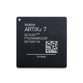
XC7A100T-1FTG256C - Artix-7 FPGA, 101K LCs, 256-FTBGA | AMD
MPN: XC7A100T-1FTG256C ✓ Active| Qty | Unit Price | Extended |
|---|---|---|
| 1 | $285 | $285.00 |
| 10 | $268 | $2,680.00 |
| 100 | $252 | $25,200.00 |
| 500 | $235 | $117,500.00 |
| 1,000 | $215 | $215,000.00 |
XC7A100T-1FTG256C Overview
An Artix-7 FPGA is a programmable logic device that occupies the mid-range slot in AMD's 7-series portfolio (Spartan-6 below, Kintex-7 above), optimized for cost-sensitive, high-throughput, power-constrained systems. The 7-series architecture shares a unified ASMBL (Advanced Silicon Modular Block) fabric across all four family members, so Artix-7 inherits 6-input LUTs, 36 Kb block RAM, DSP48E1 slices, and SelectIO with HSTL/DDR memory interfaces from Kintex-7, while trading high-speed serial transceivers for lower die cost.
Key features include up to 6.6 Gb/s transceivers on speed-grade /package permutations (the FTG256 omits GTX), integrated PCIe Gen2 hard cores, dual 12-bit 1 Msps ADCs, and clock-management tiles comprising 6 CMTs each with one PLL and one MMCM. A 1.0 V Vccint core, separate Vccaux (1.8 V) and Vcco (1.2-3.3 V HR I/O plus 1.2-1.8 V HP I/O) rails, and an Artix-7-specific power-optimization tier let designers meet thermal envelopes as low as 2-3 W at moderate toggle rates.
Typical applications span software-defined radio (SDR) front-ends, machine-vision cameras, industrial motor control and PLCs, low-cost wireless backhaul, avionics flight controllers, and medical imaging pipelines. The FTG256 package balances thermal pad access with 170 single-ended I/Os, so most industrial and instrumentation form factors can be supported without moving to larger FGG484 or FBG676 footprints.
When designing with this device, plan decoupling around the FPGA's recommended power-rail decoupling network (one 100 uF bulk per rail plus 0.1 uF + 0.01 uF close to each VRM pin). The FTG256's 1.0 mm ball pitch supports reflow with standard 4-mil NSMD or 5-mil SMD stencils; verify thermal performance with the AMD XPE spreadsheet before committing the PCB.
This page synthesizes distributor pricing, package-level drop-in alternatives, and practical Artix-7 design notes - context not duplicated in the official ds181 datasheet.
Drop-in alternatives for XC7A100T-1FTG256C — same package, pin-to-pin compatible. Different-package parts requiring PCB rework are excluded.
Variants in this series
Same-series models that are drop-in compatible with XC7A100T-1FTG256C (same form factor and footprint) — differing in Package.
Quick Comparison Tool — Select alternative parts for side-by-side comparison:
XC7A100T-2FTG256C
✅ Drop-In📋 Reference alternative (not in catalog)
XC7A100T-1FTG256I
✅ Drop-In📋 Reference alternative (not in catalog)
XC7A100T-1CSG324C
✅ Drop-In✓ In Stock
$59.9 / Unit
View Datasheet →XC7A75T-1FTG256C
✅ Drop-In📋 Reference alternative (not in catalog)
LFE5U-100F8BG756I
✅ Drop-In📋 Reference alternative (not in catalog)
XC7A100T-1FTG256C Maximum Ratings & Electrical Characteristics
| Family | Artix-7 |
| Logic Cells | 101,440 |
| Block RAM (bits) | 4,976,640 |
| Block RAM (Kb) | 4,860 |
| DSP Slices (DSP48E1) | 240 |
| Speed Grade | -1 |
| Temperature Grade | Commercial (C): 0 C to +85 C |
| Package | 256-ball FTBGA (FTG256) |
| Package Size | 17 mm x 17 mm, 1.0 mm pitch |
| User I/Os | 170 |
| CMTs (PLL + MMCM) | 6 |
| Process Node | 28 nm HPL HKMG |
| Core Voltage (Vccint) | 1.0 V nominal |
| Auxiliary Voltage (Vccaux) | 1.8 V nominal |
| Configuration Mode | Master Serial / Slave Serial / SPI / BPI / JTAG |
| RoHS Status | Compliant |
| Mounting Type | Surface Mount (BGA) |
XC7A100T-1FTG256C 17 mm x 17 mm, 1.0 mm pitch Pin Configuration Guide
Pin configuration for XC7A100T-1FTG256C (17 mm x 17 mm, 1.0 mm pitch package). This digital IC includes GPIO, communication interfaces (UART, SPI, I2C), and power pins. Refer to the manufacturer datasheet for alternate pin functions and configuration options. Essential for embedded system design and PCB layout.

No detailed pinout data available for XC7A100T-1FTG256C.
Refer to the datasheet for full pin configuration.
Typical Applications
XC7A100T-1FTG256C is suitable for 6 applications: Software Defined Radio (SDR), Machine Vision Camera Processing, Industrial Motor Control, Software Defined Wireless Backhaul, Medical Imaging Front End, Avionics Flight Control & Drones.
Software Defined Radio (SDR)
The XC7A100T-1FTG256C's 240 DSP48E1 slices and 4,976,640 bits of block RAM make it a strong fit for SDR baseband and IF processing in commercial-grade platforms. The FTG256's 170 user I/Os provide enough LVDS pairs to interface a 16-bit dual-channel ADC at up to 250 Msps for narrowband IF sampling, while the -1 speed grade meets timing for lattice-based channelizers. The 28 nm HPL process keeps typical SDR board power below 4-5 W, beating Spartan-6 perf/W by ~40%. Use MMCMs for sampling-clock synthesis and allocate spare block RAM for polyphase filterbanks. Avoid the FTG256 footprint if you need >4 Gbps serial links - that requires GTX transceivers found only on higher packages.
Recommended
Machine Vision Camera Processing
The XC7A100T-1FTG256C delivers ample logic and 240 DSP48E1 slices for real-time image processing in industrial cameras: Bayer demosaicing, color correction, and Sobel/FFT kernels run comfortably within ~60 percent of the 100T's resources at 1080p60. The FTG256's 17x17 mm body fits inside PoE-plus camera heads where board area is constrained, while 170 user I/Os accommodate MIPI-CSI, LVDS, and HD-SDI sensor inputs. Industrial-grade variants (XC7A100T-1FTG256I) extend operation into -40 C to +100 C workshops. Power optimization techniques - clock-gating, GT-disabled bitstreams, and DPRIO-mode block RAM banking - keep camera head dissipation under 3.5 W for fanless designs.
Recommended
Industrial Motor Control
Industrial motor drives benefit from the XC7A100T-1FTG256C's high DSP48E1 count for field-oriented control (FOC) loops at switching frequencies up to 50 kHz. The -1 commercial speed grade is sufficient for sinusoidal encoder interpolation when the FPGA over-samples quadrature signals; the 240 DSP slices handle 4-6 sensorless observers per device. The FTG256 exposes enough HP I/Os to drive 12-channel three-phase MOSFET gate drivers directly, while Vcco can be split between 3.3 V for logic and 1.8 V for high-speed ADCs. For harsh industrial environments, the XC7A100T-1FTG256I industrial variant supports -40 C operation. Validate temperature with the AMD XPE spreadsheet at full DSP utilization.
Recommended
Software Defined Wireless Backhaul
Low-cost wireless backhaul radios (sub-6 GHz LTE/5G small cells, TVWS, point-to-point microwave) find a sweet spot in the XC7A100T-1FTG256C's resource mix. The 101K logic cells support CPRI/SERDES interfaces at half-rate plus baseband PHY functions, while block RAM allocates happily to OFDM CP/FFT scratch buffers. The FTG256's 17 mm footprint fits in the industry-standard micro-onu form factor used in small-cell radios, and 170 I/Os support multi-radio JESD204B ADC hook-ups at 3 Gbps. The -1 commercial grade satisfies indoor and weatherproof-enclosure deployments; choose XC7A100T-1FTG256I for outdoor i-3 cabinet gear.
Recommended
Medical Imaging Front End
The XC7A100T-1FTG256C's 240 DSP slices and 4.86 Mb block RAM suit portable medical imaging - ultrasound beamforming, optical coherence tomography (OCT), and pulse-oximetry DSP pipelines. The FTG256's compact 17 mm package and 170 I/Os allow a portable handheld imaging head to integrate multiple ADCs without PCB area scaling. Decoupling rails with low-noise LDOs (TPS7A4700 family) preserves ADC dynamic range - SNR improvement of 3-5 dB over switching-only supplies is achievable. FDA/IEC 60601-1 isolation requirements dictate that any medical design uses the industrial-grade XC7A100T-1FTG256I; the commercial grade is limited to non-life-support clinical equipment.
Recommended
Avionics Flight Control & Drones
Small UAV flight controllers and Experimental aircraft attitude reference systems fit the XC7A100T-1FTG256C's resource envelope: redundant sensor arbitration (IMU + GPS + barometer + magnetometer) and Kalman filtering run comfortably in <20 percent of logic, leaving headroom for custom control laws. The FTG256's 17 mm footprint suits PC/104-class boards used in experimental avionics, while 170 I/Os support up to 4x CAN, 2x Ethernet MAC interfaces, and 8 PWM-driven motor esc lines. Pair with industrial XC7A100T-1FTG256I for -40 C to +100 C operational envelopes demanded by low-altitude flight electronics. Note that DO-254 certifiable projects require additional documentation beyond standard FPGA design packages.
Recommended
Recommended Products Summary
Engineering reference data for XC7A100T-1FTG256C — comparison, design guidance, and compliance information.
Selection Guide
Comparison with Alternatives
| Parameter | This Product | XC7A100T-2FTG256C | XC7A100T-1FTG256I | XC7A100T-1CSG324C | XC7A75T-1FTG256C | LFE5U-100F8BG756I |
|---|---|---|---|---|---|---|
| Brand | AMD | AMD | AMD | AMD | AMD | Lattice Semiconductor |
| Package | 256-ball FTBGA (FTG256) 17x17 mm | 256-ball FTBGA (FTG256) 17x17 mm - same | 256-ball FTBGA (FTG256) 17x17 mm - same | 324-ball CSBGA (CSG324) 12x12 mm | 256-ball FTBGA (FTG256) 17x17 mm - same | 256-ball BGA - cabGA variant |
| Logic Cells | 101,440 | 101,440 | 101,440 | 101,440 | 75,520 | 100K LUTs |
| DSP Slices | 240 | 240 | 240 | 240 | 180 | 196 SYS DSP blocks |
| Block RAM (bits) | 4,976,640 | 4,976,640 | 4,976,640 | 4,976,640 | 3,780,000 | 3,750,000 |
| User I/Os | 170 | 170 | 170 | 210 | 170 | 248 |
| Speed Grade | -1 | -2 | -1 | -1 | -1 | LFE5U 8G turbo |
| Temperature Grade | Commercial 0 C to +85 C | Commercial 0 C to +85 C | Industrial -40 C to +100 C | Commercial 0 C to +85 C | Commercial 0 C to +85 C | Industrial -40 C to +100 C |
Key Differentiators
- Highest logic/DSP density in 256-ball FTBGA class for cost-sensitive designs (vs XC7A75T-1FTG256C)
- Compact 17x17 mm body for high-density board designs (vs XC7A100T-1CSG324C)
- AMD Xilinx toolchain maturity including Vivado WebPACK free licensing (vs LFE5U-100F8BG756I)
Design Notes
Estimated: The Artix-7 FTG256 junction-to-ambient thermal resistance (theta_JA) for a standard 4-layer JEDEC test board is ~13 C/W with the center thermal balls connected, so a fully loaded 100T at 1 W dissipation rises only ~13 C above ambient. For sealed enclosures with limited convection, the AMD XPE spreadsheet predicts a more realistic 2-3 W steady-state power budget; add 1 mm copper clearances above the ball grid to expose the thermal balls for a heat spreader.
Decoupling per the AMD Xilinx UltraScale/7-series reference design: one 100 uF bulk capacitor + one 4.7 uF + one 0.1 uF + one 0.01 uF capacitor stack per Vccint pin pair, placed within 1 cm of the BGA balls. Vccaux requires a 4.7 uF + 0.1 uF stack per ball; Vcco banks each need 0.1 uF close to every four pins. Use 4-mil NSMD land pads on a 1.0 mm BGA pitch and standard 4-mil stencils for assembly.
Do not assume GTX transceivers are present on FTG256 - the 100T FTG256 omits GTX; only specific Kintex-7 packages expose multi-gigabit transceivers. If your design needs >500 Mbps serial links, you must select a Kintex-7 or move to a Spartan-7 with limited 1.25 Gbps SERDES, or implement LVDS-based communications. For JTAG, route TCK with a series 100-ohm termination at the FPGA end to prevent signal ringing on long scan chains.
Compliance Information
RoHS and REACH compliance per AMD product page. Not AEC-Q100 qualified - the device is for industrial / commercial systems; equivalent automotive XA7A100T variants exist on the XA prefix.