XC7K325T-2FFG900I vs XC7K410T-2FFG900I Comparison
Detailed side-by-side comparison of XC7K325T-2FFG900I by AMD and XC7K410T-2FFG900I by AMD. Compare key specifications, electrical parameters, packaging, lifecycle status, pricing, and availability to determine the best component for your design requirements.
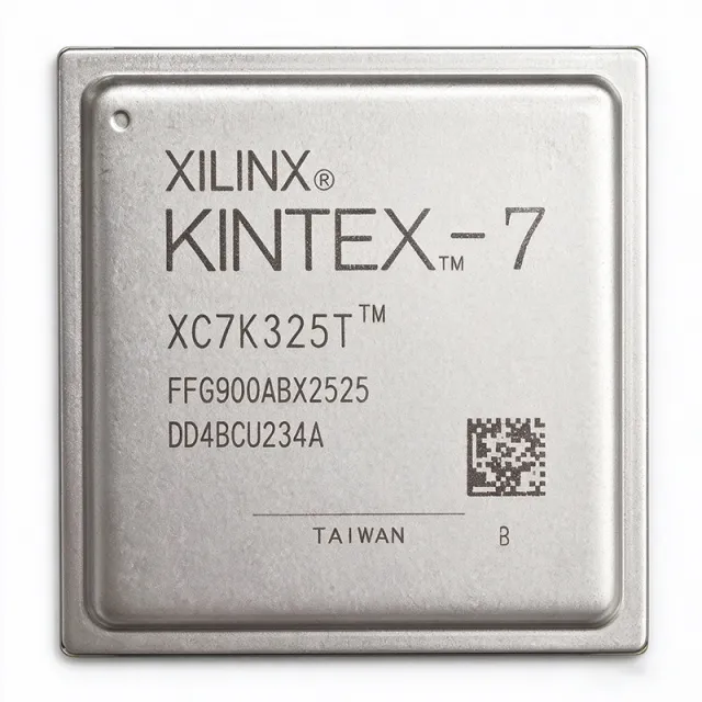

Specification Comparison
| Parameter | XC7K325T-2FFG900I | XC7K410T-2FFG900I |
|---|---|---|
| Brand | AMD | AMD |
| Category | FPGA & CPLD | FPGA & CPLD |
| Lifecycle Status | Active | Active |
| Stock Status | In Stock | In Stock |
| Unit Price (USD) | $65.00 | $920.00 |
| Family | Kintex-7 | — |
| Logic Cells | 326080 | 406,720 |
| Block RAM | 16404480 bits | 29,306,880 bits |
| DSP Slices | 840 | 1,540 |
| User I/O | 500 | — |
| Package | 900-BBGA, FCBGA | 900-BBGA, FCBGA (FFG900) |
| Speed Grade | -2 | -2 |
| Temperature Grade | Industrial (-40°C to +100°C) | — |
| Process Technology | 28nm | 28nm HPL HKMG |
| Core Voltage (VCCINT) | 1.0V | — |
| I/O Standards | LVCMOS, LVDS, HSTL, SSTL | — |
| Transceivers | 16 (GTX) | 32 (GTX) up to 12.5 Gbps |
| PCIe Support | Gen3 | Gen3 x8 |
| RoHS Status | Compliant | Compliant |
| Mounting Type | Surface Mount | Surface Mount |
| User I/O Count | — | 500 |
| Temperature Range | — | -40°C to +100°C (industrial) |
| Configuration Memory | — | SRAM-based |
| I/O Standards Supported | — | LVCMOS, LVDS, HSTL, SSTL, etc. |
| Clock Management | — | MMCM and PLL |