Verstärker-ICs
Produkte (510)

OPA827 - Low-Noise JFET Op Amp | Texas Instruments
The OPA827 is a low-noise, high-precision, JFET-input operational amplifier from Texas Instruments. It combines outstanding DC precision with excellent AC performance, featuring a maximum input offset voltage of 150 µV, a typical drift of 0.5 µV/°C, a typical input bias current of 3 pA, and very low 0.1-Hz to 10-Hz noise of 250 nVPP. The device is unity-gain stable and operates from a single or dual supply, with a wide supply range of ±4 V to ±18 V (or 8 V to 36 V single supply). It is available in 8-pin SOIC and 8-pin VSSOP packages, specified for operation from -40°C to +125°C. An operational amplifier (op amp) is a high-gain voltage amplifier with differential inputs and a single-ended output, used in signal conditioning, filtering, and instrumentation. The OPA827 belongs to the JFET-input op amp family, which offers very high input impedance and low input bias current, making it ideal for interfacing with high-impedance sources such as sensors and photodiodes. Within the hierarchy of analog ICs, it is a precision amplifier, a subset of linear amplifiers, and part of the broader signal chain IC category. Key features of the OPA827 include its low offset voltage (150 µV max), low drift (0.5 µV/°C typ), low bias current (3 pA typ), and low noise (4 nV/√Hz at 10 kHz, 250 nVPP 0.1-10 Hz). It also offers a high open-loop gain of 120 dB, a gain bandwidth product of 22 MHz, and a slew rate of 28 V/µs. The device is fully specified over the extended temperature range and is RoHS compliant. Technically, the OPA827 uses a JFET input stage to achieve its low bias current and high input impedance, while a precision bipolar output stage provides low output impedance and high drive capability. The amplifier is internally compensated for unity-gain stability, simplifying design. Its low distortion and high linearity make it suitable for high-performance audio and precision instrumentation. Typical applications include high-end audio preamplifiers and DAC output buffers, precision data acquisition systems, active filters, and sensor signal conditioning. The low noise and low bias current are particularly beneficial in photodiode amplifiers and medical instrumentation. When designing with the OPA827, ensure proper decoupling of the power supply pins with 0.1 µF ceramic capacitors placed close to the device, as recommended in the datasheet. Also, consider the input common-mode range and output swing limitations for your specific supply voltages.

OPA828 - 45MHz 36V JFET Op Amp, 4nV Noise | TI
The Texas Instruments OPA828 is a high-speed JFET-input operational amplifier delivering 45 MHz gain bandwidth product, 150 V/us slew rate, and 36 V operation with rail-to-rail output (RRO) in SOIC-8 and HVSSOP-8 (DGN) packages. It is the next-generation successor to the industry-standard OPA627 and OPA827, combining high speed with high DC precision. A JFET-input operational amplifier is a linear amplifier IC whose input stage uses junction field-effect transistors, giving it extremely low input bias current (picoampere level) while preserving the voltage-noise performance of a bipolar front end. Within the power management and signal-chain hierarchy, op amps form the core of analog signal conditioning between sensors and data converters. Key features include 4 nV/Hz input voltage noise density at 1 kHz, only 60 nVRMS of noise from 0.1 Hz to 10 Hz, 50 uV input offset voltage, and 0.45 uV/C offset drift. JFET inputs draw just 1 pA typical bias current, and MUX-friendly inputs simplify multiplexed signal chains. The wide supply range of +/-4 V and above supports 36 V single-supply operation. Architecturally, the OPA828 pairs a precision JFET input stage with a rail-to-rail output stage, enabling maximum output swing into ADCs and loads on low supply rails. Compared with the OPA627, TI documents wider bandwidth, higher slew rate, and rail-to-rail output as the key upgrade paths (per the TI comparison tool). Typical applications include photodiode transimpedance amplifiers, precision ADC driver front ends, high-fidelity audio stages, and test-and-measurement signal conditioning where low bias current, low noise, and high speed must coexist. Design consideration: ensure headroom for the JFET common-mode input range, and decouple supply pins with 0.1 uF ceramics placed within 2 mm; for TIA use, compensate feedback capacitance against input capacitance to preserve phase margin.
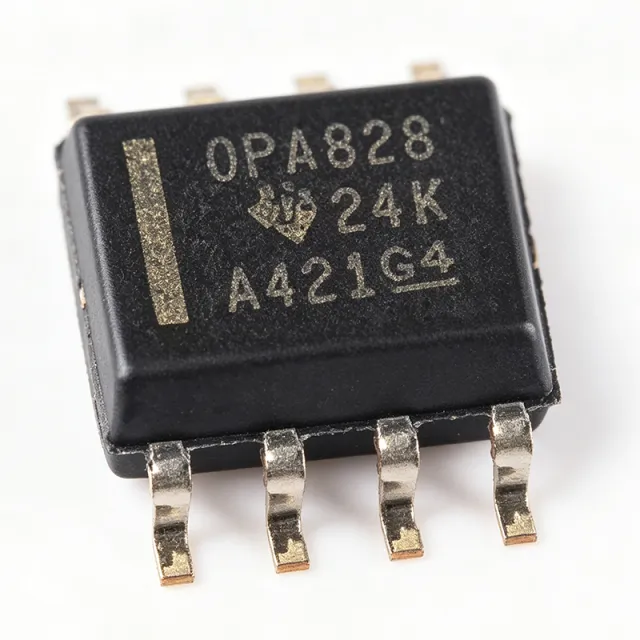
OPA828IDR - 45MHz JFET Op Amp, 4nV/√Hz | TI | Precision Amplifier
The Texas Instruments OPA828IDR is a high-speed, JFET-input operational amplifier delivering 45 MHz gain bandwidth, 150 V/us slew rate, and 4 nV/√Hz voltage noise in an 8-pin SOIC package. It operates over a wide supply range of ±4 V to ±18 V (36 V total) with rail-to-rail output (RRO), positioning it as the next-generation successor to the legendary OPA627 and OPA827 op amps. A JFET-input operational amplifier is a type of precision amplifier whose input stage uses junction field-effect transistors, providing extremely low input bias current (picoampere range) and high input impedance. Within the signal-chain hierarchy, op amps sit between sensors and data converters, serving as the general-purpose analog building block for amplification, filtering, buffering, and transimpedance conversion. Key features include 50 uV input offset voltage, 0.45 uV/C offset drift, 1 pA typical input bias current, and only 60 nVRMS of noise from 0.1 Hz to 10 Hz. These DC precision specifications make the OPA828 suitable for applications where both speed and accuracy are demanded simultaneously - a rare combination. MUX-friendly inputs allow multiplexed signal chains without settling artifacts or charge-injection damage. Architecturally, the OPA828 pairs a JFET input stage with a rail-to-rail output stage, combining classic precision topology with modern output swing. The RRO output maximizes dynamic range in low-voltage systems while the 36 V supply rating supports traditional ±15 V industrial analog rails without redesign. Typical applications include photodiode transimpedance amplifiers (TIA), high-fidelity audio front ends, precision ADC and DAC buffer stages, and active filters in test and measurement instrumentation. The wide 36 V supply range is particularly valuable for industrial designs retaining legacy ±15 V rails. For design, ensure supply decoupling with 0.1 uF ceramic capacitors placed within 3 mm of each supply pin. When replacing an OPA627, verify compensation and bias-current paths, as community feedback shows some legacy TIA circuits require adjustment despite pin compatibility. This page synthesizes distributor pricing, drop-in alternatives, and practical design notes not found in the manufacturer datasheet.

OPA858QIDSGRQ1 - 5.5GHz FET-Input TIA Op-Amp Q1 | TI
The Texas Instruments OPA858QIDSGRQ1 is an automotive-qualified (AEC-Q100), wideband, low-noise decompensated operational amplifier with FET (CMOS) inputs, delivering a 5.5-GHz gain bandwidth product (GBWP) while remaining stable at a minimum gain of 7 V/V. It is supplied in a compact 8-pin WSON (2x2 mm) surface-mount package. A decompensated amplifier is an operational amplifier internally compensated for stable operation only above a minimum closed-loop gain (here 7 V/V). By removing the compensation for unity-gain stability, the decompensated topology achieves dramatically higher bandwidth and lower input-referred noise than unity-gain-stable amplifiers of comparable process technology. In the signal-chain hierarchy, the OPA858-Q1 sits as a wideband voltage-feedback amplifier serving transimpedance amplifier (TIA) and high-gain voltage amplifier roles in high-speed analog front ends. Key features include the 5.5-GHz GBWP that enables high closed-loop bandwidths at transimpedance gains in the range of tens to hundreds of kilo-ohms, FET inputs that minimize input bias current effects on photodiode and high-impedance nodes, and single-ended single-channel configuration optimized for high-speed signal paths. The Q1 variant is manufactured on TI automotive flows and is qualified per AEC-Q100, supporting automotive lidar, imaging, and test applications that demand supply-chain traceability and automotive-grade reliability. The architecture combines CMOS input devices with wideband voltage-feedback internals, yielding low input capacitance that is critical in TIA designs because photodiode plus amplifier input capacitance directly limits achievable bandwidth per unit of transimpedance gain. TI provides the OPA858 together with a companion evaluation module and application collateral covering feedback resistor selection, compensation capacitor sizing, and stability analysis. Typical applications include automotive lidar receiver TIAs, wideband photodiode amplification in optical sensing, high-speed voltage amplification stages, and wideband test and measurement front ends. The device suits any signal chain that requires gain of 7 V/V or higher with multi-hundred-megahertz to gigahertz-class bandwidth. Design consideration: because the amplifier is only stable at gain >= 7 V/V, noise-gain analysis must be performed at all frequencies, including input capacitance effects at the inverting node; verify phase margin with the TI datasheet stability curves before finalizing feedback-network values.

PAM8302A - 2.5W Filterless Class-D Mono Audio Amplifier | Diodes Incorporated
The Diodes Incorporated PAM8302A is a 2.5 W filterless Class-D mono audio amplifier housed in an 8-pin MSOP package, with an additional SOP-8 option. Its CMOS architecture drives 4 ohm or 8 ohm speakers directly without low-pass output filters, saving PCB area and BOM cost while delivering high-quality, low-THD audio reproduction. An audio amplifier is an electronic integrated circuit that boosts a low-power audio input signal to a level capable of driving a loudspeaker or headphones. The Class-D topology uses pulse-width modulation (PWM) to switch the output transistors fully on or fully off, achieving much higher efficiency (typically >85%) than linear Class-AB amplifiers (typically <60%). Within the broader taxonomy, the PAM8302A sits in the audio amplifier IC category, a subset of amplifier ICs, which belong to the signal chain and power management product families. Filterless Class-D amplifiers are particularly valued in portable, battery-powered designs because they eliminate bulky LC output filter networks, reducing both board area and cost. Key specifications include a 2.5 W continuous output power into 4 ohm at 10% THD from a 5.5 V supply, low THD+N of 0.10% at 1 W into 8 ohm, a wide 2.0 V to 5.5 V supply range, integrated undervoltage lockout at 2.1 V, and a low shutdown current. The MSOP-8 (with thermal pad) footprint offers a compact 3.0 mm x 3.0 mm outline suitable for handheld devices, while the SOP-8 (PAM8302AADCR) variant serves designs requiring through-hole-compatible footprints. Built-in short-circuit protection and thermal shutdown further enhance robustness in consumer applications. The PAM8302A employs a fully-differential PWM modulator with proprietary filterless modulation, which eliminates the traditional LC reconstruction filter while maintaining acceptable EMI through controlled edge-rate switching and spread-spectrum techniques. The differential input topology also rejects common-mode noise from upstream audio DACs or PWM sources. Typical applications include portable Bluetooth speakers, handheld gaming consoles, alarm clocks, intercom systems, toys, and any cost-sensitive battery-powered device requiring moderate audio output. Designers frequently choose this part for retrofit audio upgrades in retro gaming hardware, single-board computers, and IoT devices where PCB area is at a premium. When designing with the PAM8302A, ensure adequate power supply bulk decoupling (typically 10 uF) close to the AVDD/PVDD pins to minimize THD. The SD pin (active-low shutdown) must be tied high for normal operation or controlled via a GPIO for power sequencing. Reserve sufficient copper pour on the exposed thermal pad to dissipate Class-D switching losses, especially at full 2.5 W output. This page synthesizes distributor pricing, verified drop-in alternatives, and application-specific design notes not found in the manufacturer datasheet alone, making it a practical engineering reference for sourcing and design.

PAM8403 - 3W Filterless Class-D Stereo Audio Amplifier | Diodes Incorporated
The Diodes Incorporated PAM8403 is a 3 W filterless Class-D stereo audio amplifier delivered in a 16-pin SOP package, operating from a 2.5 V to 5.5 V single supply. Each channel delivers 3 W into a 4 ohm load at 10% THD+N with a 5 V power supply, while maintaining efficiency up to 90% thanks to the Class-D switching topology. The device integrates a bridge-tied load (BTL) output stage that removes the need for external LC low-pass filters on the speaker lines, saving PCB area and BOM cost in stereo and mono consumer audio designs. A Class-D audio amplifier is a switching amplifier topology that uses pulse-width modulation at a switching frequency far above the audio band to recreate the input waveform. Compared with Class-AB linear amplifiers, Class-D parts achieve much higher efficiency (often >85%), which reduces power dissipation in portable and battery-powered applications. The PAM8403 belongs to the audio amplifier IC family, which itself sits inside the broader amplifier IC and integrated circuit hierarchy used in consumer and prosumer audio products. Key features include low THD+N for high-quality sound reproduction, a typical 90% efficiency figure that extends battery life in portable applications, and integrated protection such as short-circuit and thermal shutdown. The shutdown pin (SD) can drive the amplifier into a low-current mute state, and the device also provides a noise-free power-up/power-down cycle that eliminates audible pops. Available only in the SOP-16 package, the part is aimed at compact stereo speaker implementations where board real estate is at a premium. Typical applications include LCD TV and monitor speaker drivers, portable and Bluetooth speaker enclosures, laptop docking stations, DVD and game console line outputs, and phone / speakerphone accessories. Its filterless architecture allows very short, direct PCB traces from the IC outputs to the speakers, simplifying the layout versus traditional Class-D solutions that need an LC reconstruction filter. When designing with the PAM8403, place the supply decoupling capacitors as close to the VDDP and VDDL pins as possible, use a ferrite bead on the speaker outputs if extra EMI suppression is required, and respect the maximum junction temperature rating to avoid thermal shutdown during sustained high-output conditions. This page synthesizes distributor pricing, verified drop-in alternatives, and practical design notes that are not found in the standalone manufacturer datasheet PDF, including PCB layout and EMI considerations specific to filterless Class-D designs.

PGA206UA - 5MHz FET-Input Programmable Gain In-Amp | TI
The Texas Instruments PGA206UA is a high-speed digitally programmable gain instrumentation amplifier (PGA) delivering a 5 MHz bandwidth, 100 pA maximum FET-input bias current, and digitally selectable gains of 1, 2, 4, and 8 V/V in a 16-pin SOIC (SOL-16) surface-mount package. A programmable gain instrumentation amplifier is a precision differential amplifier whose closed-loop gain is set by digital control inputs rather than external resistors. It sits within the amplifier hierarchy as an instrumentation amplifier -> precision op amp -> analog front-end (AFE) -> signal chain IC, combining a true three-architectural-input instrumentation amplifier front end with internally switched gain networks. PGAs are essential in data acquisition systems where a single amplifier must handle sensor signals spanning several orders of magnitude without manual range switching. Key features include fast settling to 0.01% after a gain change, +/-40V input protection that survives overrange faults common in industrial field wiring, and a low maximum offset voltage of 1.5 mV. The FET input stage keeps bias current at 100 pA max, preserving accuracy with high-impedance sources such as pH probes, photodiodes, and piezoelectric sensors. Technically, the PGA206 uses internally switched precision resistor networks controlled by two digital gain-select lines, a scheme the datasheet notes pairs naturally with an external logic latch to acquire gain data from a high-speed digital bus. Slew rate is 25 V/us and the supply range is +/-4.5V to +/-18V, allowing operation from standard +/-5V, +/-12V, or +/-15V analog rails. Operation is specified from -40C to +85C. Typical applications include multi-range data acquisition front ends, programmable sensor interfaces, test and measurement instrumentation, and dynamic signal conditioning where gain must change on-the-fly between measurements. Design consideration: total response time after a gain change equals the switching time plus the settling time to the new output voltage, so budget for settling in high-throughput scanning systems. This page synthesizes distributor pricing, drop-in alternatives, and practical design notes not found in the manufacturer datasheet.
PGA207UA - 5MHz Programmable Gain Instrumentation Amp | TI
The Texas Instruments PGA207UA is a high-speed digitally programmable gain instrumentation amplifier offering a 5 MHz bandwidth, 100 pA maximum FET-input bias current, and digitally selectable gains of 1, 2, 5, and 10 V/V, housed in a 16-pin SOIC (SOL-16) surface-mount package. A programmable gain instrumentation amplifier (PGIA) is a precision differential amplifier whose closed-loop gain is set digitally rather than by external resistors. In the signal-chain hierarchy it sits between sensors and data converters, combining the true instrumentation-amplifier input stage (high common-mode rejection, balanced high-impedance inputs) with gain-switching logic, so a single ADC channel can resolve signals spanning several orders of magnitude. Key features of the PGA207 include two CMOS/TTL-compatible address lines for gain selection, analog inputs internally protected against overloads up to +/-40V even with the supplies off, and laser-trimmed offset voltage for low drift. A fast 0.01% settling specification allows the gain to be switched between conversions in high-throughput data-acquisition systems without dead time. Architecturally, the device uses a three-amplifier instrumentation topology with FET input transistors, giving negligible input bias current (100 pA max) for high-source-impedance sensors, a 25 V/us slew rate, and 18 nV/sqrt(Hz) input noise with 75 dB CMRR. Laser trimming at the Burr-Brown production line holds offset voltage to 1.5 mV max, preserving accuracy at the lowest gains. Typical applications include programmable data-acquisition front ends, dynamic signal ranges from PT100 sensors and strain-gauge bridges, test and measurement instrumentation, and industrial process-control analog front ends feeding 12- to 16-bit ADCs. When designing, remember the gain lines are logic-level inputs: tie them to clean CMOS/TTL levels and route away from the input traces. The +/-40V input protection removes the need for external clamp diodes in most industrial environments. This page consolidates distributor pricing, drop-in family alternatives, and engineering design guidance not found in a single manufacturer datasheet page.
PGA207UA/1K - 5MHz Programmable Gain In-Amp | Texas Instruments
The Texas Instruments PGA207UA/1K is a high-speed, digitally programmable gain instrumentation amplifier delivering gains of 1, 2, 5, and 10 V/V with a 5 MHz bandwidth, a FET input stage with 100 pA maximum bias current, and a 16-pin SOL-16 SOIC surface-mount package. A programmable gain instrumentation amplifier (PGIA) is a precision differential amplifier whose closed-loop gain is set digitally rather than by external resistors. Within the signal-chain hierarchy, it sits between raw transducers and ADCs as a front-end conditioning device, combining the high input impedance and CMRR of a true three-op-amp instrumentation amplifier with gain-switching logic that lets one device serve multiple transducer full-scale ranges. Key features of the PGA207UA/1K include digitally selectable gains (1, 2, 5, 10 V/V) via two CMOS/TTL-compatible address lines, fast settling to 0.01%, a FET input with maximum bias current of 100 pA, and internal input protection rated for plus/minus 40V overloads even with power supplies off. The device is laser-trimmed for low offset voltage (1.5 mV max) and low drift, eliminating manual calibration in most data acquisition designs. Technically, the PGA207 architecture uses a true instrumentation amplifier input stage whose gain is switched by the two digital address lines, so no external gain resistors are needed and gain accuracy is factory-determined. The 5 MHz bandwidth at higher gains supports multiplexed data acquisition channels, while the FET input minimizes loading on high-impedance sources such as photodiodes and piezoelectric sensors. Supply operation spans plus/minus 4.5V to plus/minus 18V, with a slew rate of approximately 25 V/us. Typical applications include multiplexed data acquisition front ends, programmable test and measurement signal conditioning, and industrial sensor interfaces where input channels of different amplitude must share one ADC. Fast settling allows channel-to-channel switching without long dead time, improving system throughput. Design consideration: ensure supply headroom within the plus/minus 4.5V to plus/minus 18V range and route the digital gain-select lines away from the high-impedance inputs to prevent digital noise coupling into the analog front end. This page synthesizes distributor pricing, drop-in family alternatives, comparison data, and practical design notes not found in the manufacturer datasheet.

PGA281 - Zero-Drift Programmable Gain Instrumentation Amplifier | TI
The PGA281 is a high-precision instrumentation amplifier from Texas Instruments featuring digitally-controllable gain and signal-integrity test capability. It uses proprietary autozeroing techniques to achieve low offset voltage, near-zero offset and gain drift, excellent linearity, and nearly no 1/f noise. The device is available in a 16-pin TSSOP package (PW) and operates over a wide supply range, making it suitable for precision sensor interfaces and data acquisition systems. An instrumentation amplifier (INA) is a type of differential amplifier that amplifies the difference between two input signals while rejecting common-mode voltages. It is characterized by high input impedance, high common-mode rejection ratio (CMRR), and low offset voltage. The PGA281 belongs to the family of programmable gain instrumentation amplifiers (PGIAs), which allow the gain to be set digitally or via external resistors, providing flexibility in signal conditioning chains. This category sits within the broader hierarchy of analog amplifiers, which are essential building blocks in electronic systems for signal conditioning and measurement. Key features of the PGA281 include gain programmable from G = 0.2 to 10,000 using an external resistor, fully differential outputs with integrated clamping, low offset voltage of 10 µV (typ) and 35 µV (max), low offset drift of 0.1 µV/°C (typ) and 0.3 µV/°C (max), and low input bias current of 5 pA (typ). These specifications make it ideal for high-accuracy applications where drift and noise are critical. The PGA281 employs a zero-drift architecture that continuously corrects offset and drift, achieving near-zero temperature coefficients. The integrated clamping circuitry protects the outputs from overvoltage conditions, enhancing system robustness. The device supports a wide supply range, typically ±5V, and provides rail-to-rail output swing, maximizing dynamic range. Typical applications include precision current sensing (10 µA to 100 mA), sensor signal conditioning for bridge sensors, thermocouple amplifiers, and data acquisition front-ends. Its low offset and drift make it suitable for medical instrumentation, industrial process control, and test and measurement equipment. When designing with the PGA281, ensure proper decoupling of the power supply pins and consider the thermal performance of the TSSOP package. The gain-setting resistor should be a precision resistor to maintain gain accuracy. The device's signal-integrity test capability allows for system-level diagnostics, which is valuable in safety-critical applications.

SGM8955XN5G - Zero-Drift Op Amp, 1-Ch, SOT-23-5 | SG Micro
The SG Micro SGM8955XN5G is a single-channel, micro-power, CMOS zero-drift operational amplifier housed in a 5-pin SOT-23-5 (XN5) surface-mount package. It delivers a 22 µV (MAX) offset voltage with 80 nV/°C offset drift, 100 dB open-loop gain, and 130 pA input bias current, optimized for precision signal chains operating from low-voltage rails. An operational amplifier (op amp) is a high-gain differential DC amplifier that uses external feedback components to set gain, bandwidth, and transfer characteristics. Zero-drift op amps employ either chopper or auto-zero (chopper-stabilized) architectures to continuously correct offset voltage, eliminating the 1/f flicker noise and offset drift that plague conventional CMOS and bipolar input stages. The SGM8955 belongs to the precision amplifier category within the broader linear IC hierarchy: operational amplifier → amplifier IC → analog signal chain → semiconductor. Key features of the SGM8955XN5G include a 20 µA typical quiescent supply current, 180 V/ms slew rate, rail-to-rail input and rail-to-rail output (RRIO) swing, EMI filtering/RF suppression on the inputs, and an integrated auto-zero calibration loop. The SOT-23-5 (XN5) package operates across -40 °C to +125 °C and supports supply voltages suitable for 2.7 V-5.5 V single-supply systems. The combination of low offset, low drift, low power, and RRIO makes the part a strong fit for battery-powered instrumentation, transducer conditioning, and precision ADC front ends. The SGM8955/6 architecture uses a chopper-stabilized CMOS input stage to achieve sub-50 µV offset, eliminating the periodic recalibration required by conventional CMOS amplifiers in precision applications. The internal EMI/RF input filter rejects high-frequency interference, simplifying PCB layout for sensor applications in electrically noisy environments. The 20 µA quiescent current and low shutdown leakage allow the part to remain continuously powered in battery applications without significantly reducing runtime. Typical applications include high-precision ADC driver circuits, weigh scale and strain gauge signal conditioning, thermocouple and bridge sensor amplifiers, portable medical instrumentation, battery-powered industrial sensors, and zero-drift transducer interfaces. The RRIO capability allows the part to operate at unity gain in single-supply systems where input and output signals swing close to either supply rail. When designing with the SGM8955XN5G, place the input capacitor as close to the op-amp input pins as possible, ensure the feedback network uses 1% or better resistors to maintain gain accuracy, and add an anti-aliasing RC network at the output when driving a downstream ADC. Estimated: total supply current is the sum of the 20 µA quiescent plus the load-dependent output stage current. This page synthesizes distributor pricing, drop-in alternatives, and practical design notes not found in the manufacturer datasheet.

SI8921BD-IS4 - ±250 mV Isolated Amplifier, 5 kV | Skyworks
The Skyworks Solutions SI8921BD-IS4 is a galvanically isolated analog amplifier with a ±250 mV differential input range, 5.0 kV RMS isolation rating, and differential output, housed in a wide-body stretched SOIC-8 package. Key headline specifications include 0.8 µs signal delay, ±0.40 µV typical input offset, ±0.06% typical gain error, 0.5 µV/°C offset drift, and -9 ppm/°C typical gain drift, providing accurate current-shunt measurement across industrial temperature ranges. An isolated amplifier is a type of analog amplifier that combines a precision front-end differential amplifier with a galvanic isolation barrier, transferring the signal across the barrier through capacitive or transformer coupling. The isolation barrier protects low-voltage control circuitry from high-voltage common-mode transients on the field side, enabling safe measurement of floating signals such as those present across current-shunt resistors in motor drives, solar inverters, and uninterruptible power supplies. Within the broader hierarchy, an isolated amplifier belongs to the isolation IC family, which includes digital isolators and isolated gate drivers - all of which form essential building blocks in power-management and industrial-automation systems requiring reinforced insulation per IEC 60747-17 and UL 1577. The SI8921BD-IS4 features a specified input range of ±250 mV, well suited for direct connection across low-ohm shunt resistors in high-current paths. Its differential output swings to a 2.5 V peak full-scale signal, which can be fed directly into the ADC front-end of a motor controller or power-conversion MCU. The device's low offset and drift specifications eliminate the need for periodic calibration in many systems, while its 0.8 µs propagation delay supports closed-loop current control in fast-switching converters. Architecturally, the SI8921BD-IS4 integrates a precision chopper-stabilized input amplifier, a sigma-delta modulator, an isolation capacitor barrier, and a differential output decoder on the low-voltage side. The internal LDO regulators on both sides of the barrier simplify power-supply design - the high-side is powered from a 3.0 V to 5.5 V supply, and the low-side is powered independently from 3.0 V to 5.5 V. The CMOS output stage is capable of driving 2 kΩ loads with low distortion. Typical applications include current-shunt monitoring in three-phase motor drives, photovoltaic inverter string-current sensing, UPS battery-current measurement, industrial process-control isolation, and high-voltage rail monitoring in telecom rectifiers. The differential output interfaces directly with SAR ADCs and sigma-delta converters found in C2000 and PIC32 families. When designing with this device, place bypass capacitors of 0.1 µF and 1 µF close to both VDDA and VDDD pins, keep the input traces short and balanced to preserve CMRR, and observe the creepage and clearance rules of the wide-body SOIC-8 footprint to maintain the 5 kV isolation rating. The differential output should be routed as a matched pair to avoid common-mode pickup in noisy switching environments. This page synthesizes distributor pricing, drop-in alternatives, and practical design notes not found on a single manufacturer product page or distributor listing.

SSM2141PZ - Differential Line Receiver, 100dB CMR, 3MHz | ADI
The Analog Devices SSM2141PZ is an integrated differential line receiver (audio amplifier, Class AB) designed to receive balanced line inputs in professional audio applications requiring high noise immunity and optimum common-mode rejection. Housed in an 8-pin PDIP (PZ) package, it operates from dual supplies of ±6V to ±18V and typically achieves 100 dB of common-mode rejection (CMR) at DC and 60 Hz, far exceeding the ~40 dB CMR achievable with a generic op amp and four discrete precision resistors. The device delivers 0.001% typical THD, a fast 10 V/us slew rate, and a wide 3 MHz small-signal bandwidth. A balanced line receiver is a specialized analog building block that accepts a differential signal riding on a common-mode voltage (such as the long cable run from a stage to a mixing console) and converts it to a single-ended, ground-referenced output while rejecting the common-mode noise picked up along the way. In the audio signal chain hierarchy, the SSM2141 sits between the input connector / XLR stage and downstream ADC or line-level processing; it is part of the broader family of audio amplifiers and instrumentation amplifiers used in pro-audio and broadcast equipment. Key differentiating specifications include 100 dB CMR (DC, typ), 70 dB CMR at 20 kHz and 62 dB at 40 kHz, 0.001% THD+N, 10 V/us slew rate, 3 MHz bandwidth, and a 600 ohm minimum load. Internal thin-film resistor networks are laser-trimmed to deliver matching that no off-the-shelf 0.1% discrete resistor approach can match at production volume, which is what enables the headline CMR figure. Typical applications include balanced audio line receivers in mixing consoles and stage boxes, AES3 / EBU receiver front-ends, audio distribution amplifiers, and instrumentation front-ends where high DC and AC common-mode rejection is required. The 600 ohm load rating and +22 dBu headroom make it directly compatible with broadcast and studio analog line-level standards. When designing with the SSM2141PZ, treat the gain-setting resistor (typically 10 kohm between pins 1 and 8 for unity gain) as a low-noise, low-drift metal-film part to preserve CMR. Add 100 ohm series output resistors plus 10 nF to ground at each output if cable capacitance will exceed ~1000 pF, to prevent oscillation. Decouple both supply pins with 0.1 uF ceramic in parallel with 10 uF tantalum or electrolytic, placed within 5 mm of the package. This page synthesizes distributor pricing, drop-in alternatives, and practical PCB layout notes not found in the manufacturer datasheet alone, including cross-brand substitutes from Texas Instruments and Maxim that share the same 8-pin PDIP footprint and equivalent CMR-class performance.
SSM2142 - Balanced Audio Line Driver, 10 Vrms/600Ω | Analog Devices
The Analog Devices SSM2142 is an integrated differential-output buffer amplifier that converts a single-ended input signal to a balanced (differential) output pair with high output drive capability. Housed in a 16-pin SOIC (or PDIP variant) package, it delivers a transformer-like balanced output capable of driving 10 V RMS into a 600 Ω load, making it a single-chip replacement for discrete audio line-driver circuits that historically required audio output transformers. A balanced line driver, or differential-output audio amplifier, is a specialized analog IC that takes an unbalanced single-ended input and produces two anti-phase outputs whose common-mode noise is rejected by the downstream differential receiver. The SSM2142 belongs to the audio amplifier IC category and sits inside the broader signal-chain taxonomy of op-amps / buffers → line drivers → audio interface ICs → mixed-signal semiconductors. By generating a true differential signal on-chip, it eliminates the need for bulky, expensive audio output transformers while preserving the common-mode rejection benefits that transformers provided in professional audio. Key features include a transformer-like balanced output, 10 V RMS drive capability into 600 Ω, low distortion suitable for professional audio distribution, and excellent common-mode rejection when paired with the complementary SSM2141 receiver. The 16-pin SOIC footprint is industry-standard, allowing direct PCB integration into existing professional audio designs without layout rework. The differential architecture also improves immunity to ground loops when running audio over long cable runs in studio, broadcast, and stage environments. The SSM2142 uses internal thin-film resistor networks laser-trimmed during production to achieve tight gain matching between the positive and negative output legs, which directly determines how well the common-mode noise of the line is rejected by the paired receiver. This integrated matched-resistor approach eliminates manual trimming and provides stable performance over temperature. The amplifier can drive the full pro-audio level of +24 dBu (12.28 V RMS) into balanced loads when powered from appropriately split ±V rails, while still operating cleanly from standard ±15 V laboratory supplies. Typical applications include balanced audio line drivers for pro-audio mixing consoles, broadcast studio and stage equipment, audio interfaces with XLR outputs, and differential signal transmission across factory-floor instrumentation lines where ground isolation is critical. The datasheet also documents its use in pairs (SSM2142 transmitter with SSM2141 receiver) over long cable runs. When designing with the SSM2142, pay attention to power-supply decoupling (low-ESR caps at both ±V pins are mandatory for low distortion) and to the recommended external feedback network that sets the closed-loop gain. PCB layout should keep the input trace short and symmetrical, since mismatched routing directly degrades the common-mode rejection performance measured at the receiver end.
SSM2143PZ - Audio Differential Line Receiver, 90dB CMR | Analog Devices
The Analog Devices SSM2143PZ is an integrated differential amplifier (line receiver) intended to receive balanced audio line inputs in professional and prosumer audio applications requiring high common-mode noise immunity. Housed in an 8-pin PDIP (PZ) through-hole package, it is specified for a typical common-mode rejection of 90 dB at DC and 60 Hz, dropping to 85 dB at 20 kHz, achieved by laser-trimming on-chip resistors to better than 0.005%. An audio line receiver is the front-end gain stage that converts a balanced, twisted-pair analog signal — typically carried on XLR or TRS cable runs — into a single-ended ground-referenced signal that downstream ADC, mixing, or amplifier stages can use. Its defining role is rejecting common-mode noise (mains hum, RF pickup, ground-loop voltage) that appears equally on both signal lines while preserving the differential audio content. Receivers such as the SSM2143PZ therefore sit at the top of the analog signal-path hierarchy: transducer -> line receiver -> ADC/mixer -> power amplifier -> speaker. Key features include an ultra-low total harmonic distortion of 0.0006% typical at 1 kHz (less than 0.004% across the full audio band), a fast 10 V/us slew rate, and a wide 7 MHz small-signal bandwidth. The device operates from dual supplies of ±6 V to ±18 V (single supply 6 V to 36 V) and draws only 2.7 mA quiescent supply current. The input stage handles signals as large as +28 dBu at the nominal G = 1/2 configuration, allowing direct connection to professional +4 dBu consoles without external attenuation. Although optimized for G = 1/2, a gain of 2 is realized by reversing the +IN/-IN and SENSE/REFERENCE connections. The SSM2143 architecture combines a precision operational front-end with four on-chip laser-trimmed thin-film resistors that set the gain and provide the matched impedance ratio required for high CMR. Internal overdrive clamping protects downstream stages when large common-mode or differential transients appear on the line, eliminating the need for external protection diodes in most studio and stage installations. Typical applications include balanced audio line receivers in mixing consoles, microphone preamplifier inputs, A/D converter driver stages in audio digitizers, broadcast and recording-studio equipment, and stage-box interfaces for live sound. Its high CMR also makes it well suited to industrial instrumentation where long cables carry small analog signals in electrically noisy environments. When designing with the SSM2143PZ, route input traces as a tightly coupled, length-matched pair and place 0.1 uF supply-decoupling capacitors within 5 mm of the supply pins. The device is specified for operation from -40 C to +85 C and remains RoHS-compliant; the SOIC-8 (S) variant should be selected for reflow-compatible SMT designs. This page synthesizes distributor pricing, parametric cross-references, and PCB-level design guidance for the SSM2143PZ beyond what the manufacturer datasheet alone provides.

SSM2166SZ - Microphone Preamplifier w/ Variable Compression | ADI
The Analog Devices SSM2166SZ is a complete microphone conditioner IC that integrates a low-noise microphone preamplifier, a voltage-controlled amplifier (VCA), and a variable compression/noise-gate control loop in a single 14-pin narrow-body SOIC (NSOIC) package. The part provides a unity-gain microphone preamp front-end with adjustable gain followed by a dynamic compression block whose compression ratio and rotation point are user-programmable via external resistors, plus an adjustable-threshold noise gate that mutes the output below a settable floor to suppress ambient hum and breath noise. A microphone preamplifier with variable compression and noise gating is a specialized audio signal-chain block used to capture speech or instrument signals with wide dynamic range and deliver them at a controlled level to downstream ADCs, codecs, mixers, or transmitters. Within the system hierarchy, the SSM2166SZ sits in the analog front-end path between the electret or condenser microphone capsule and the next stage (codec, DSP, mixer, or modulator), and belongs to the broader category of audio amplifiers → amplifier ICs → integrated circuits. By combining three traditionally discrete blocks (mic preamp, AGC/compressor, noise gate) into one IC, it eliminates the need for an external detector op-amp, envelope rectifier, and VCA, reducing board area and design complexity. Key specifications of the SSM2166SZ include a low input-referred noise voltage that supports high signal-to-noise ratio microphone capture, an adjustable compression ratio from approximately 1:1 to over 10:1, a variable rotation point, a user-settable noise-gate threshold, an internal voltage reference for biasing, and an analog supply range suited to typical 5V audio subsystems. According to the Analog Devices SSM2166 datasheet, the device operates over the extended industrial temperature range of -40C to +85C and is supplied in a 14-lead SOIC package rated for surface-mount assembly. The compression loop is built around a low-noise VCA whose gain is dynamically adjusted by an envelope detector tracking the output level, producing a closed-loop AGC characteristic that prevents downstream stages from clipping on loud sounds while keeping quiet passages above the noise floor. Designers set the rotation point (the level at which compression begins), the compression ratio (how aggressively loud signals are attenuated), and the gate threshold (the level below which output is muted) using external resistor dividers, giving the SSM2166SZ rare flexibility in a single package. Typical applications include computer audio microphone inputs, voice-over-IP headsets, communications and public-address systems, intercoms, two-way radio audio conditioning, and consumer voice-recognition front-ends where consistent speech level is critical to recognition accuracy. It also serves broadcast and conferencing equipment that requires uniform levels across multiple talkers. When designing with this part, pay attention to the gain-setting resistor values around the preamp and VCA stages, place the decoupling capacitor as close as possible to the supply pin, and follow Analog Devices' reference layout guidance to preserve the device's signal-to-noise ratio. Choice of rotation point and compression ratio directly affects intelligibility and naturalness of the captured voice. This page synthesizes distributor pricing, drop-in alternatives, and practical design notes not found in the manufacturer datasheet alone, with cross-references verified against the latest DigiKey and Mouser listings as of 2026-10-10.
STK443 - 2Ch 5-25W AF Power Amp Hybrid IC | SANYO
The SANYO STK443 is a 2-channel (stereo) audio-frequency power amplifier built as a thick-film hybrid integrated circuit, delivering 5 W to 25 W minimum per channel into typical loudspeaker loads. It is supplied in a single inline SIP package with 10 formed leads, designed to be mounted through-hole on the amplifier PCB alongside its own heatsink tab. The STK443 was developed for low-cost split-supply consumer audio products where a compact, self-contained output stage simplifies board layout versus discrete complementary-pair designs. An AF (audio-frequency) power amplifier is the final active stage in an audio reproduction chain that drives a loudspeaker from a low-level signal source such as a preamplifier, mixer, or DAC output. Hybrid AF power ICs integrate input and driver transistors, output power devices, and biasing components on a single ceramic substrate, distinguishing them from monolithic silicon audio ICs by their higher output power, higher supply voltage tolerance, and larger physical footprint. Within the broader component taxonomy, the STK443 belongs to the amplifier IC category, which itself is a subset of analog signal-chain ICs and ultimately of power management and signal-conditioning semiconductors. The STK443 features a typical output of 2 x 25 W at low THD into a defined load impedance, operates over a wide supply range, and includes internal thermal protection. The dual-channel monolithic front end is followed by discrete power transistors mounted on the same substrate, a topology that lets the device source peak current demands while remaining economically viable for mass-produced stereo equipment. Built-in short-circuit and over-temperature shutdown protect the output stage against common fault conditions seen in consumer amplifiers. Typical applications for the STK443 include home stereo amplifiers, integrated A/V receivers, karaoke mixing amplifiers, powered speaker systems, and musical instrument practice amplifiers. It is also found in automotive head-unit audio outputs and as a retrofit replacement module in legacy SANYO-designed equipment where the original STK-series hybrid has failed and a same-form-factor part is required to avoid PCB rework. When designing with the STK443, observe the recommended heatsink thermal resistance and mounting torque to keep the substrate within its rated junction temperature under sustained full-power operation. Bypass supplies close to the module's VCC pins and use the recommended Zobel RC network across each output to maintain stability with reactive speaker loads. This page synthesizes distributor availability, parametric drop-in alternatives, and practical design notes gathered from SANYO documents and aftermarket datasheets not typically aggregated by catalog distributors.

SY88803VKG - 155Mbps PECL Limiting Post Amplifier | Microchip
The Microchip Technology (formerly Micrel) SY88803VKG is a 3.3V/5V, 155Mbps PECL low-power limiting post amplifier with a TTL Loss-of-Signal (LOS) output, housed in a 10-pin MSOP package. It is designed specifically for fiber-optic receiver front ends that follow a transimpedance amplifier (TIA). A limiting post amplifier is the second stage in an optical receiver signal chain. The linear signal output from a TIA can contain significant amounts of noise and may vary widely in amplitude; a limiting amplifier converts this small, noisy differential signal into a clean, fixed-amplitude logic-level PECL data stream, restoring signal integrity before clock-and-data-recovery (CDR) circuitry. In the hierarchy of optical receiver electronics, it sits between the TIA and the CDR/serializer, and is a form of special-purpose high-speed amplifier IC. Key features include single 3.3V or 5V supply operation to 155Mbps, low-noise PECL differential data outputs, a chatter-free TTL Loss-of-Signal output, a TTL /EN enable input for power management, and a programmable LOS assertion threshold. Low power consumption suits compact optical modules such as OC-3/STM-1 and Fast Ethernet transceivers. Architecturally, the device uses a cascade of wideband differential gain stages with automatic offset compensation; the saturating output stages guarantee constant output swing regardless of input amplitude above sensitivity. The programmable LOS threshold lets designers match the trip point to the optical module sensitivity budget, and the chatter-free hysteresis design prevents false LOS toggling near threshold. Typical applications include 155Mbps fiber-optic receivers, SDH/SONET OC-3 line cards, Fast Ethernet (100Base-FX) optical modules, and industrial fiber links. It connects directly to typical TIAs, making it a drop-in signal-chain element. Design consideration: route the differential PECL outputs as 50-ohm controlled-impedance pairs and decouple the supply pins close to the package to keep jitter low; verify the LOS threshold setting against the TIA output amplitude range. This page synthesizes distributor pricing, drop-in alternatives, and practical design notes not found in the manufacturer datasheet.

TAS5827 - 47W Stereo Closed-Loop Class-D Amp | TI
The TAS5827 is a stereo high-performance, closed-loop Class-D audio amplifier with an integrated audio processor and support for up to 192-kHz audio. It delivers 47W per channel in BTL mode and is housed in a 32-pin VQFN (5x5 mm) package. The device features a digital input interface, making it ideal for modern digital audio systems. A Class-D amplifier is a switching amplifier that uses pulse-width modulation to achieve high efficiency, often exceeding 90%, compared to linear amplifiers. It is a key component in the audio signal chain, converting digital audio data into high-power analog output while minimizing heat dissipation. The TAS5827 integrates a closed-loop architecture, which improves linearity and reduces distortion, and an audio processor for advanced signal processing. Key features include a delay buffer up to 5ms in BTL mode or 10ms in PBTL mode, Class-H control for enhanced efficiency, and hardware control mode for selecting switching frequency, analog gain, BTL/PBTL mode, and cycle-by-cycle current limit threshold via pin configuration. The device also supports software control mode with classic BQs, 3-band DRC, AGL, and proprietary audio envelope tracking Class-H control. The TAS5827 uses a closed-loop feedback design that reduces power supply noise and improves audio quality. It integrates a high-performance audio processor capable of executing complex DSP algorithms, making it suitable for applications requiring EQ, DRC, and dynamic range compression. The device operates from a single supply and includes comprehensive protection features. Typical applications include smart speakers, soundbars, home theater systems, and active speakers. Its high efficiency and low power dissipation make it ideal for battery-powered and energy-conscious designs. The integrated audio processor reduces external component count, simplifying system design. When designing with the TAS5827, ensure proper PCB layout for thermal management and minimize parasitic inductance in the output stage. Use appropriate decoupling capacitors on the power supply pins and follow the recommended layout in the datasheet for optimal performance.
TAS5827RHBR - 43W Stereo Digital Class-D Amp | Texas Instruments
The Texas Instruments TAS5827RHBR is a 43-W stereo, digital-input, closed-loop Class-D audio amplifier with integrated audio processing and Class-H control. Housed in a 32-pin VQFN (RHB) package measuring 5x5 mm, this device delivers high-efficiency amplification for a wide range of consumer and professional audio applications. It supports a supply voltage range of 4.5V to 26.4V and operates over a temperature range of -40°C to 85°C. A Class-D amplifier is a switching amplifier that uses pulse-width modulation (PWM) to achieve high efficiency, often exceeding 90%, compared to linear amplifiers. The TAS5827 integrates a closed-loop architecture that reduces distortion and improves power supply rejection, making it suitable for high-fidelity audio systems. The digital input interface accepts I2S, TDM, and other digital audio formats, simplifying system design by eliminating the need for external DACs. Key features include a 43-W output power per channel into 4-ohm loads, integrated audio processor with biquad filters and dynamic range compression, and Class-H control that optimizes power supply voltage for efficiency. The device also supports multiple switching frequencies and offers cycle-by-cycle current limit protection. Its closed-loop design ensures low THD+N and high signal-to-noise ratio, critical for premium audio performance. The TAS5827 uses a digital audio processing core that can be configured via I2C or hardware control mode. In hardware mode, switching frequency, analog gain, BTL/PBTL mode, and current limit threshold are set via pins, eliminating the need for software driver integration. This flexibility makes it easy to deploy in systems where firmware development is not desired. Typical applications include smart speakers, soundbars, home theater systems, and automotive audio. The high efficiency reduces heat dissipation, enabling compact designs without large heatsinks. The integrated audio processor allows designers to implement EQ, crossover, and dynamic range control without external DSP. When designing with this device, ensure proper PCB layout with adequate ground planes and decoupling capacitors near the power pins. The thermal pad must be soldered to a copper area for heat dissipation. Also, consider the input signal format and configure the device accordingly for optimal performance.
TAS6754QDKQRQ1 - Automotive 4-Ch Class-D Audio Amp | TI
The TAS6754QDKQRQ1 is an automotive-grade, four-channel digital-input Class-D audio amplifier from Texas Instruments, offered in a 56-pin HSSOP (DKQ) package with exposed thermal pad. It implements 1L modulation, requiring only one inductor per BTL channel, and operates from a 19V supply with a 2MHz switching frequency. The device integrates current sense and real-time DC/AC load diagnostics for robust automotive speaker fault detection. A Class-D audio amplifier is a switching amplifier that converts a digital or analog audio signal into a high-frequency pulse-width modulated square wave, which is then low-pass filtered to reconstruct the audio. Class-D topologies achieve high efficiency (typically 80-90%) because the output transistors operate as switches, minimizing power dissipation compared to linear Class-AB amplifiers. In automotive audio systems, this efficiency reduces heat-sinking requirements and extends the available audio power from the vehicle's electrical system. Key features include four independent audio channels, 1L modulation that removes four inductors versus traditional designs, 2MHz switching for compact output filters, integrated current sense, and DC/AC real-time load diagnostics. The 19V rated supply is aligned with automotive audio power rails, and the AEC-Q100 Q1 suffix qualifies the device for automotive applications. The 56-pin HSSOP package supports surface-mount assembly with an exposed thermal pad for heat removal. 1L modulation is a proprietary Class-D scheme that uses a single inductor per bridge-tied-load channel, reducing system cost and size. The 2MHz switching rate moves the switching fundamental well above the audio band, simplifying the output low-pass filter and lowering out-of-band emissions. Integrated current sense and real-time load diagnostics monitor speaker health, enabling fault detection for shorts, opens, and degradation. The digital input accepts common automotive digital audio formats, eliminating the need for a separate DAC and analog front end. Typical applications include automotive infotainment head units, external amplifier modules, EV pedestrian warning (AVAS), telematics/eCall audio, rear-seat entertainment, and commercial-vehicle audio. The device is especially suited for designs where four channels of clean audio must be delivered from a 19V rail with minimal inductor count and integrated diagnostic coverage. When designing with the TAS6754QDKQRQ1, provide sufficient copper area on the exposed thermal pad and keep the output LC filter close to the device to minimize EMI. Verify the digital audio source timing and protocol against the datasheet before PCB layout.

TDA18214AHN/C1,557 - Silicon TV Tuner IC DVB-T | NXP
The NXP Semiconductors TDA18214AHN/C1,557 is a high-performance silicon tuner IC designed for digital terrestrial and digital cable TV reception, controlled via an I2C serial interface and housed in a 40-pin HVQFN (6x6 mm) exposed-pad package. The part delivers a Low IF (LIF) output signal to an external demodulator and supports all major digital TV standards including DVB-T. A silicon tuner is an integrated RF receiver front-end that replaces the can-tuned varactor modules used in legacy analog televisions. Within the receiver signal chain hierarchy, it sits at the top: antenna or cable input -> silicon tuner (RF amplification, image-reject mixing, channel filtering) -> Low IF output -> demodulator IC -> transport stream. Because tuning, gain control, and filtering are all implemented on-chip, the TDA18214 family dramatically reduces board area, BOM count, and factory alignment effort compared with discrete tuner designs. Key features of the TDA18214AHN include single-conversion architecture delivering a Low IF signal, full I2C bus control for channel selection and gain programming, support for all digital terrestrial and cable TV standards (DVB-T, DVB-C, ISDB-T, ATSC, DTMB families), and an exposed-pad 40-HVQFN package suitable for compact set-top box and TV main boards. Surface-mount construction supports standard reflow assembly. Architecturally, the TDA18214 integrates a low-noise RF amplifier, image-reject downconversion mixer, broadband synthesizer, and channel-selection filtering in a single CMOS/BiCMOS die. Delivering LIF directly to the demodulator eliminates SAW-filter-heavy IF stages in many designs, and the digital-controlled gain distribution optimizes linearity versus noise figure across the received channel. Typical applications include digital set-top boxes, integrated digital TV (iDTV) main boards, USB TV tuner dongles, PC-TV capture cards, and cable/terrestrial hybrid receivers. Its broad standards support lets one design serve multiple regional markets with firmware changes only. Design consideration: as a 6x6 mm HVQFN with exposed pad, the thermal and ground path depends on the PCB land pattern; the exposed pad must be soldered to a solid ground plane with thermal vias, and the I2C bus requires proper pull-up sizing for reliable 100/400 kHz communication. This page synthesizes distributor availability data, drop-in alternatives, and practical design notes not found in the manufacturer datasheet. Note that this part is marked Obsolete (last buy March 31, 2016; last delivery June 30, 2016), so availability is limited to remaining distributor and broker stock as of 2026-10-11.

TDA2009A - 10W+10W Stereo Class-AB Audio Amplifier | STMicroelectronics
The STMicroelectronics TDA2009A is a class-AB dual Hi-Fi audio power amplifier assembled in a Multiwatt® package, delivering 10 W + 10 W of continuous output power per channel into 8 Ω loads (stereo operation from 8 V to 28 V supply). The device is specially designed for high quality stereo applications such as Hi-Fi music centers, mini-component stereos, multimedia speaker systems, and instrument amplifiers that demand dual-channel output from a single, well-protected IC. What is a class-AB audio power amplifier? A class-AB amplifier is the most common bipolar topology used in mid-power audio reproduction; it biases its output stage so that push and pull transistors each conduct for slightly more than half a cycle. This eliminates the crossover distortion of pure class-B designs while keeping efficiency far higher than class-A. The TDA2009A instantiates that topology with on-chip short-circuit protection, thermal shutdown, and AC short-circuit protection of the load, integrating a complete stereo driver into one Multiwatt-11 power package with the heatsink tab on the back. Key features include 10 W + 10 W continuous output into 4 Ω with THD = 10 % at 14 V / 4 Ω (per ST datasheet), 1 % THD typical at lower levels, an operating supply range of 8 V to 28 V, 3 A peak output current per channel, very low harmonic and crossover distortion, and internal protection against short circuits, thermal overload, and DC voltage on the load. The Multiwatt-11 (Pentawatt-style) package exposes a metal tab so the part itself forms the heatsink, simplifying PCB mechanical design. The architecture uses a vertical bipolar power process with quasi-complementary NPN/PNP output pairs, a unity-gain inverting topology per channel, and internal bias generators that minimize quiescent crossover glitch. The result is a flat frequency response from 20 Hz to 20 kHz with low 0.1 % harmonic content, suitable for full-range music reproduction without complex external compensation networks. Typical applications include stereo Hi-Fi music centers, multimedia speaker systems, TV audio output stages, guitar and instrument practice amplifiers, automotive radios (with 14 V supply), and self-powered USB speakers where dual-channel audio from a single chip replaces two single-channel modules. When designing with this device, place a 100 nF decoupling capacitor on the supply pin as close as possible to the IC, use feedback resistors of 39 kΩ for closed-loop gain near 35 dB, and provide adequate heatsinking through a clip-on or bonded tab. The package tab is electrically tied to the -Vs pin (or to the substrate in some legacy datasheets) - consult the datasheet pinout before insulating the heatsink. This page synthesizes distributor pricing, drop-in compatible alternatives, and practical design notes for the TDA2009A, providing information not consolidated on any single distributor product page.
TDA7297 - 15W+15W Dual Bridge Amplifier | STMicroelectronics
The STMicroelectronics TDA7297 is a dual bridge Class-AB audio amplifier delivering 15W+15W output power in a 15-pin Multiwatt package, designed specifically for TV and portable radio applications. It operates from a wide 6V to 18V supply range and uses an internally fixed gain topology that eliminates the need for SWR capacitors, bootstrap networks, and Boucherot cells. A Class-AB (dual bridge) audio amplifier is a topology that combines two push-pull output stages in a bridge-tied-load (BTL) configuration, allowing higher output swing across a speaker load without large DC-blocking capacitors. The TDA7297 belongs to the broader category of integrated audio power amplifiers, which sit within the analog signal chain and power management domains in a typical consumer electronics design. Dual-bridge configurations are especially valued in compact consumer devices because they double the voltage swing across the speaker and remove the need for a bulky output coupling capacitor. Key features include 15W per channel continuous output into 8 ohm loads, low standby current with a dedicated Standby pin, and a Mute function for click-free power-up sequencing. The device integrates all output transistors in the same silicon die and requires only a few external resistors and a power supply bypass network, enabling very compact PCB designs. Typical THD at 1W output is in the 0.1%-0.5% range, making it suitable for entry-level TV audio, multimedia monitors, and portable boombox designs. The internally fixed gain topology simplifies board layout but limits design flexibility compared to externally adjustable amplifiers like the TDA7294. Thermal performance is handled through the Multiwatt-15 package, which exposes the die tab to a vertical heatsink profile with through-hole pins for robust mechanical mounting. Designers must still respect the safe operating area at high ambient temperatures where sustained 2x15W output can push the junction close to thermal limits without adequate heatsinking. Typical applications include flat-panel TV stereo speaker drivers, portable radio boombox amplifiers, LCD monitor audio outputs, PC motherboard sound subsystems, and DIY audio upgrade kits. The part is commonly found in 2.1-channel subwoofer + satellite systems where a third mono channel can be derived by bridging the two outputs in parallel. When designing with the TDA7297, always provide adequate heatsinking through the Multiwatt tab and respect the 6V-18V supply range. The Standby and Mute pins should be sequenced with a 10kohm/10uF RC network as recommended in the datasheet to achieve click-free power transitions.