Speicher-ICs
Unterkategorien
Produkte (459)

MT41K64M16TW-107 AUT:J - 1Gbit DDR3L SDRAM 933MHz | Micron
The Micron Technology MT41K64M16TW-107 AUT:J is a 1Gbit DDR3L SDRAM memory IC organized as 64M x 16 bits, operating at 933 MHz with 20 ns access time, housed in a 96-ball FBGA (8 x 14 mm) package. The AUT:J suffix denotes Micron's automotive-grade temperature offering, making this part suitable for extended-temperature designs. DDR3L SDRAM (Low-Voltage Double Data Rate 3 Synchronous Dynamic Random Access Memory) is a type of volatile memory IC that stores data dynamically and requires periodic refresh. Within the memory hierarchy, DDR3L sits between legacy DDR2 and DDR4, offering higher bandwidth and lower operating voltage (1.35 V nominal, backward compatible with 1.5 V DDR3 operation) at reduced power consumption. It remains one of the most widely deployed DRAM standards in embedded and industrial systems. Key features of the MT41K64M16TW-107 include the 1Gbit density in a x16 organization, a 933 MHz clock rate corresponding to DDR3L-1866 speed grade, and the compact 96-ball FBGA footprint that conserves PCB area. The parallel interface supports burst lengths of 8 with on-die termination (ODT) and 8-bit prefetch architecture per the DDR3L protocol. Technically, the device uses Micron's DRAM core process with a bank architecture supporting concurrent activation, CAS latency programming, and programmable refresh rates. The AUT grade option extends operating temperature capability beyond the commercial range for automotive and harsh-environment applications. Typical applications include automotive infotainment and ADAS buffer memory, industrial control HMI memory, networking equipment line-card buffering, and embedded processor (FPGA or MPU) main memory where DDR3L controllers are integrated. A key design consideration is signal integrity: DDR3L fly-by routing, length matching, and ODT calibration are essential at 933 MHz; refer to the manufacturer datasheet for IBIS models and layout guidelines. This page synthesizes distributor pricing, drop-in alternatives, and practical design notes not found in the manufacturer datasheet.

MT42L16M32D1HE-18 - 512Mb LPDDR2 SDRAM 134-VFBGA | Micron
The Micron Technology MT42L16M32D1HE-18 is a 512Mbit Mobile LPDDR2 SDRAM memory IC organized as 16M x 32, operating from a 1.2V supply at data rates up to 1066 MT/s (533 MHz clock) and housed in a 134-ball VFBGA package measuring 10 x 11.5 mm. LPDDR2 (Low Power Double Data Rate 2) is a JEDEC-defined memory standard derived from the DDR SDRAM family, optimized for battery-powered and thermally constrained systems. As a class of DRAM (itself a subclass of volatile memory within the broader power-management-aware memory hierarchy), LPDDR2 reduces core and I/O voltage, adds low-power states such as self-refresh and deep power-down, and integrates initialization and calibration features on-die. Key features of the MT42L16M32D1HE include its x32 bus width for high peak bandwidth per package, 1.2V VDD and VDDQ operation that minimizes dynamic power, and support for clock-stop, power-down, and self-refresh modes that cut standby consumption. The -18 speed grade corresponds to a 533 MHz clock / 1066 MT/s data rate, and the die-level LPDDR2 command interface (CA bus) reduces pin count versus conventional DDR interfaces. Architecturally, the device uses an internal bank organization with on-chip DLL-off operation support and voltage-temperature derating logic, allowing reliable operation across automotive-grade temperature ranges. Micron implements the LPDDR2 S2 die (1.2V core) with AC timing tuned for the -18 bin; signal integrity is supported by on-die termination strategies defined in the JEDEC LPDDR2 specification. Typical applications include smartphone and tablet application-processor memory, automotive infotainment and ADAS buffering (with the AUT:E AEC-Q100 variant), industrial HMI buffers, and networking line-card frame buffers. The 16M x 32 organization suits systems needing wide bursts per row activation. Design consideration: LPDDR2 fly-by-free point-to-point routing still requires length-matched CA/DQ traces and careful VDDQ decoupling; always confirm the speed-grade derating tables at your maximum junction temperature. This page synthesizes distributor availability, same-package family alternatives, and practical design notes not found in the manufacturer datasheet. Pricing references are as of 2026-09-02.
MT42L32M32D1HE-18 - 1Gbit LPDDR2 SDRAM 533MHz | Micron
The Micron Technology MT42L32M32D1HE-18 IT:D is a 1Gbit mobile LPDDR2 SDRAM memory IC organized as 32M x 32, operating at 533 MHz from a 1.2V core supply (with 1.8V I/O option), housed in a 134-ball VFBGA package measuring 10 x 11.5 mm. This industrial-grade (IT) DRAM delivers high-bandwidth parallel memory for embedded systems. LPDDR2 (Low Power Double Data Rate 2) is a JEDEC-standard SDRAM family derived from mobile DDR memory, optimized for low power consumption and high density in battery-powered and thermally constrained systems. Within the memory hierarchy, LPDDR2 sits between classic LPDDR1 and LPDDR3, introducing a 1.2V core voltage and CA (command/address) pin multiplexing that reduces pin count and simplifies PCB routing. Key features of this device include the 1Gbit density in a single x32 organization, 533 MHz data rate operation (LPDDR2-1066 class), the compact 134-VFBGA (10 x 11.5 mm) footprint, and an industrial operating temperature range appropriate for the IT grade suffix. The D suffix in the ordering code indicates lead-free, RoHS-compliant manufacturing. From an architectural standpoint, the device implements LPDDR2-S4 (standard DRAM) protocol with multiplexed command/address inputs, programmable burst lengths, and multiple low-power modes including deep power-down, self-refresh, and partial-array self-refresh, allowing system designers to trade standby current against wake-up latency. Bank interleaving sustains effective bandwidth close to the theoretical peak during real workloads. Typical applications include industrial controllers requiring high-speed working memory, embedded computing modules, automotive infotainment platforms (using the AAT automotive variant), networking equipment buffers, and test and measurement instrumentation. The x32 bus width provides wide, low-latency access well suited to processors without memory controllers optimized for narrow x16 DRAM. A key design consideration is signal integrity at 533 MHz: match CA and DQ trace lengths within the processor memory controller guidelines, and follow the VFBGA ball-map fan-out recommendations in the Micron datasheet. Power delivery must support simultaneous switching currents with adequate bulk and ceramic decoupling on both VDD1 (1.2V) and VDD2 rails. This page synthesizes distributor pricing tiers, drop-in alternatives, comparison tables, and practical design notes not found in the manufacturer datasheet, providing engineers with sourcing and design context in a single reference.

MT47H32M16NF-25E:H - 512Mb DDR2 SDRAM 400MHz FBGA-84 | Micron
The Micron Technology MT47H32M16NF-25E:H is a 512 Mbit DDR2 SDRAM organized as 32M x 16, operating at 400 MHz clock frequency with 400 ps data-output jitter specification, supplied in an 84-ball FBGA (8 x 12.5 mm) package. DDR2 SDRAM (Double Data Rate Type Two Synchronous Dynamic Random Access Memory) is a class of DRAM that transfers data on both the rising and falling edges of the clock, doubling effective bandwidth relative to SDR SDRAM at the same clock rate. In the memory hierarchy, DDR2 SDRAM sits between DDR1 and DDR3, forming part of the broader DRAM -> volatile memory -> semiconductor memory family used as main memory in embedded and computing systems. Key features of the MT47H32M16NF-25E family include a 1.8V core supply, 400 MHz operation (DDR2-800 data-rate class given the -25E speed grade), on-die termination (ODT), auto-precharge functionality, and a data mask (DM) function for write masking. The x16 organization with 16-bit data bus simplifies board-level routing in cost-sensitive embedded designs that do not need the full 64-bit wide memory bus of PC-class DIMMs. The architecture uses a 4-bank organization with burst lengths of 4 and 8, programmable CAS latency, and Posted CAS with additive latency to improve command bus efficiency. Differential strobes (DQS/DQS#) provide precise data capture timing at the controller, and the 400 ps output jitter figure supports reliable source-synchronous timing closure at full speed. Temperature variants include commercial (0C to +85C), industrial IT (-40C to +95C), automotive AAT/AIT grades, with the :H suffix denoting lead-free/RoHS-friendly ball metallurgy. Typical applications include legacy industrial controllers, networking equipment line cards, set-top boxes, medical instrumentation, and embedded processor memory subsystems built around controllers that support DDR2-800 x16 devices. Design consideration: FBGA ball packages require X-ray or acoustic inspection for solder-joint quality and exact footprint adherence to JEDEC ball maps; verify controller ODT settings against the datasheet termination table. This page synthesizes distributor pricing, drop-in alternatives, and practical design notes not found in the manufacturer datasheet.
MT47H64M16NF-25E - 1Gb DDR2 SDRAM 400MHz x16 | Micron
The Micron Technology MT47H64M16NF-25E is a 1Gbit DDR2 SDRAM memory IC organized as 64M x 16, operating at a 400 MHz clock (DDR2-800 data rate, 400 ps) in an 84-ball FBGA (8 mm x 12.5 mm) package. DDR2 SDRAM (Double Data Rate 2 Synchronous Dynamic Random Access Memory) is a type of DRAM that transfers data on both rising and falling edges of the clock, doubling bandwidth compared to DDR1 at the same clock frequency. Within the memory hierarchy it sits as a main-memory component: DRAM -> synchronous DRAM -> DDR SDRAM -> DDR2 SDRAM, used between a processor/memory controller and mass storage. DDR2 introduced a 4n-bit prefetch architecture and on-die termination (ODT) relative to DDR1. Key features of the MT47H64M16NF-25E include 8 internal banks, a 4n-bit prefetch architecture, VDD and VDDQ of 1.8V +/-0.1V with JEDEC-standard SSTL_18-compatible I/O, differential data strobe (DQS/DQS#) support, duplicate output strobe (RDQS) option, data mask (DM) functionality, auto precharge, and dynamic on-die termination that reduces signal reflections on high-speed buses. Technically, the -25E speed grade runs at DDR2-800 (CL5 at 400 MHz), with the x16 organization giving a 16-bit wide data bus for a peak bandwidth of 1.6 GB/s per device. The E die revision and FBGA (NF) package provide reliable ball-bond interconnects suitable for automated assembly. The IT suffix on the industrial variant extends the operating range to -40C to +95C. Typical applications include embedded processor and SoC main memory, industrial control and networking equipment, set-top boxes, test instrumentation, and legacy DDR2 controller designs requiring proven JEDEC DDR2 interface compatibility. When designing with this device, use SSTL_18 terminated layouts with length-matched address/command traces and reference VREF at VDD/2; the ODT settings must be programmed to match board impedance to preserve signal integrity at 400 MHz. This page synthesizes distributor pricing, drop-in DDR2 alternatives from Micron, SK Hynix, Samsung and Nanya, and practical DDR2 design notes not found in the manufacturer datasheet.
MT53B128M32D1DS-053 AUT:A - 4Gbit LPDDR4 1.866GHz | Micron
The Micron Technology MT53B128M32D1DS-053 AUT:A is a 4Gbit automotive-grade LPDDR4 SDRAM memory IC organized as 128M x 32, operating at up to 1.866 GHz (1866 MHz data rate, 3.5 ns clock cycle) from a 1.1V core supply, housed in a 200-ball WFBGA (10 mm x 14.5 mm) package rated from -40C to +125C. LPDDR4 (Low Power Double Data Rate 4) is a JEDEC-defined mobile DRAM standard optimized for low operating voltage and low power consumption. Within the memory hierarchy, LPDDR4 SDRAM sits under the volatile DRAM family as the power-optimized branch of synchronous DRAM, widely used where battery life and thermal budgets dominate design decisions. Unlike DDR4 for servers, LPDDR4 reduces interface voltage and adds deep power-down and per-bank refresh features. Key features of this device include the 4Gbit density in a x32 organization suited to processors without 16-bit memory controllers, the -053 speed bin supporting 1866 MHz operation, and automotive AEC-Q100 qualification indicated by the AUT prefix with a -40C to +125C operating range. Micron characterizes the LPDDR4 family for ultra-low power consumption to extend battery life. Architecturally, the device uses a dual-channel-capable LPDDR4 interface with dynamic frequency scaling support, low-voltage swing termination (LVSTL) I/O, and programmable drive strengths. The 1.1V VDD core with a separate 1.1V VDDQ interface minimizes I/O switching power, and self-refresh modes retain data during system idle states. Typical applications include automotive infotainment and ADAS platforms, industrial HMI and edge-compute modules, and high-performance embedded processors requiring 32-bit wide memory buses. Design consideration: LPDDR4 requires controller-side training of read/write leveling and DQS oscillator counts during initialization; verify your SoC memory controller supports the -053 (1866 MHz) speed bin timing parameters before layout. This page synthesizes distributor availability, same-family drop-in speed-grade and temperature-grade alternatives, and practical design notes not consolidated in the manufacturer part catalog.
MT53B128M32D1DS-062 - 4Gbit LPDDR4 SDRAM 1.6GHz | Micron
The Micron Technology MT53B128M32D1DS-062 is a 4Gbit mobile LPDDR4 SDRAM memory IC organized as 128M x 32, operating at 1600 MHz (DDR-3200 data rate) from a 1.1V core supply, housed in a 200-ball WFBGA (10 x 14.5 mm) package. LPDDR4 (Low Power Double Data Rate 4) is a JEDEC-defined synchronous DRAM interface standard optimized for mobile and battery-powered systems. Compared with standard DDR4 SDRAM, LPDDR4 lowers the core voltage to 1.1V, uses a point-to-point channel architecture, and introduces features such as deep power-down, per-bank refresh, and low-power idle states that reduce standby current. In the memory hierarchy, it sits within the SDRAM family of volatile semiconductor memories, falling under the broader categories of DRAM and memory ICs. Key features of this device include the 4Gbit density in a x32-wide organization that simplifies 32-bit bus designs, the -062 speed grade supporting a 1600 MHz clock for high memory bandwidth, and a compact 200-ball fine-pitch BGA footprint suited to space-constrained boards. Micron speed-grade and temperature suffixes define operating ranges across commercial and industrial conditions. Architecturally, the die implements LPDDR4 bank groups, burst lengths of 8 and 16, and programmable refresh schemes that balance bandwidth against power. The 1.1V VDD core, combined with VDDQ I/O termination optimization, minimizes dynamic power during burst transfers, while DPD (deep power down) allows microamp-level standby in always-on mobile designs. Typical applications include smartphone and tablet application-processor memory, embedded Linux gateways and routers, automotive infotainment and ADAS compute modules (using the AUT variant), and industrial edge-AI vision modules where 4Gbit capacity and LPDDR4 bandwidth are required. Design consideration: LPDDR4 requires careful length-matched routing and controller training for read/write leveling; verify the controller supports x32 LPDDR4 and confirm the speed-grade suffix matches your thermal environment before finalizing the BOM. This page synthesizes distributor pricing, same-family drop-in variants, and practical design notes not found in the manufacturer datasheet. Pricing references are as of 2026-09-02.
MT53B256M32D1DS-062 - 8Gb LPDDR4 SDRAM 3200MT/s | Micron
The Micron Technology MT53B256M32D1DS-062 is an 8Gbit Mobile LPDDR4 SDRAM memory component organized as 256M x 32, operating at a 1.6 GHz clock frequency (LPDDR4-3200 class data rate), housed in a 200-ball WFBGA (10 x 14.5 mm) fine-pitch ball grid array package. LPDDR4 (Low Power Double Data Rate 4) is a JEDEC-defined mobile DRAM standard optimized for high bandwidth and low power in battery-operated and thermally constrained systems. In the memory hierarchy, it sits as a main-memory DRAM component below cache SRAM and above storage NAND, serving as the working memory directly attached to application processors, SoCs, and FPGAs. Key features of this device include the 8Gbit density in a single-die package, a wide 32-bit data bus, LPDDR4 core operation from a nominal 1.1V supply, and low-voltage signaling (VDDQ 1.1V class) that reduces I/O power compared with DDR3L. The -062 speed grade denotes a 625 ps clock cycle (1.6 GHz clock, 3200 MT/s data rate), enabling peak bus bandwidth of approximately 12.8 GB/s per 32-bit channel. Architecturally, the device uses an 8n-prefetch banked DRAM core with burst lengths of 16 (BL16), on-die termination, and LPDDR4 power-down and self-refresh modes for aggressive idle-power management, making it suitable for sustained memory bandwidth workloads with duty-cycled power profiles. Typical applications include mobile handset main memory, embedded vision and edge-AI SoC memory, automotive infotainment and ADAS platforms, networking appliances, and FPGA-based processing systems requiring high-bandwidth low-power DRAM. A key design consideration is signal integrity on the CA and DQ buses: LPDDR4 routing requires length-matched fly-by or point-to-point topologies, controlled impedance, and accurate read/write training in the memory controller, so PCB stack-up and SoC memory-controller support must be confirmed early. This page synthesizes distributor pricing, drop-in grade variants, and practical design notes not found in the manufacturer datasheet alone.
MT53B256M32D1NP-062 - 8Gb LPDDR4 SDRAM 1.6GHz | Micron
The Micron Technology MT53B256M32D1NP-062 is a Mobile LPDDR4 SDRAM memory IC delivering 8Gbit density organized as 256M x 32, running at 1.6 GHz (LPDDR4-3200 data rate), housed in a 200-ball WFBGA package measuring 10 x 14.5 mm with a 0.5 mm ball pitch. LPDDR4 (Low Power Double Data Rate 4) is a type of synchronous DRAM standardized by JEDEC and optimized for mobile and embedded systems, offering higher bandwidth and lower power than standard DDR4. Within the memory hierarchy - LPDDR3, LPDDR4, LPDDR5 - the LPDDR4 generation balances performance and efficiency, making it the mainstream choice for smartphones, tablets, AI edge devices, and embedded computing modules that require fast access to large working sets. Key features of the MT53B256M32D1NP-062 include a wide 32-bit data bus, dual supply rails of 1.1V (VDD1) and 1.8V (VDD2) with 1.1V I/O, and support for deep power-down and self-refresh modes that minimize standby current in battery-powered designs. Bank group architecture improves random-access performance, while on-die features and JEDEC LPDDR4 compliance ensure interoperability with a broad range of SoC memory controllers. Technically, this device uses Micron's advanced DRAM process technology to achieve high data rates at low active power. The -062 speed grade supports 1.6 GHz operation. The device operates over a case temperature range of -30C to +85C (WT speed/temp variant), suiting both consumer and industrial environments. The 200-WFBGA package provides a compact, low-profile footprint that facilitates high-density PCB designs in space-constrained products. Typical applications include flagship smartphone and tablet main memory, AI edge inference accelerators, automotive infotainment, industrial controllers, and embedded logging/computing modules where real-time video processing and machine learning workloads demand high memory bandwidth per watt. When designing with this device, place decoupling capacitors close to the VDD1/VDD2 power balls and follow Micron's datasheet layout guidelines: length-match and route the high-speed CA and DQ buses with controlled impedance to preserve signal integrity at 3200 MT/s. This page synthesizes distributor pricing, drop-in alternative analysis, and practical design notes not found in the manufacturer datasheet.
MT53D1024M32D4DT-046 - 32Gbit LPDDR4 DRAM 2.133GHz | Micron
The Micron Technology MT53D1024M32D4DT-046 is a 32Gbit LPDDR4 SDRAM memory IC organized as 1G x 32, operating at 2133 MHz (LPDDR4-4266 data rate) and housed in a 200-ball VFBGA (10 mm x 14.5 mm) package. LPDDR4 (Low Power Double Data Rate 4) is a JEDEC-defined class of synchronous dynamic RAM optimized for mobile, embedded, and battery-powered systems. Within the memory hierarchy, LPDDR4 sits in the DRAM family alongside DDR4 and GDDR; its defining trait is a low-voltage interface (1.1V VDD2/VDDQ core and I/O rails for LPDDR4 operation) and power-saving features such as deep power-down, per-bank refresh, and low-power self-refresh. LPDDR4 is the dominant main-memory technology in smartphones, tablets, automotive infotainment, and edge-AI compute modules. Key features of the MT53D1024M32D4DT-046 include 32Gbit density in a single die, a 32-bit wide data bus, 2133 MHz clock operation (4266 MT/s), a built-in temperature sensor, auto precharge, write leveling, ZQ calibration, asynchronous reset, and data mask functionality. The WT:D grade of this part supports -40C to +95C operation, while AAT:D variants extend to +105C for automotive and industrial environments. Architecturally, the device uses an 8n-prefetch DRAM core with dual-channel operation, supporting burst lengths of 16 and on-the-fly access modes. The unified LPDDR4/LPDDR4X die design means the same silicon can run at 1.1V VDDQ (LPDDR4 mode) or 0.6V VDDQ (LPDDR4X mode), allowing board designers to future-proof layouts for lower-power LPDDR4X migrations. Typical applications include smartphone and tablet main memory, automotive infotainment and ADAS domains, edge-AI compute modules, industrial gateways, and networking equipment where high bandwidth per watt is critical. Design consideration: LPDDR4 fly-by routing requires length-matched 4-layer-plus PCB stacks with on-die termination (ODT) tuning; always validate controller compatibility for the specific speed bin (-046 = 2133 MHz). This page synthesizes distributor pricing, drop-in alternatives, and practical design notes not found in the manufacturer datasheet.
MT53D1024M32D4DT-046 AUT:D - 32Gbit LPDDR4 DRAM | Micron
The Micron MT53D1024M32D4DT-046 AUT:D is an automotive-grade 32 Gbit mobile LPDDR4/LPDDR4X SDRAM with a 1 Gbit x 32 I/O organization, 1866 MHz (4266 MT/s class) operation, and a 200-ball WFBGA (approximately 10 x 14.5 mm) package rated from -40 C to +125 C ambient for automotive deployments. LPDDR4 (Low Power Double Data Rate 4) is a mobile DRAM standard of the SDRAM family of volatile memory ICs. It uses a low-voltage interface (1.10 V VDDQ for LPDDR4, 0.60 V VDDQ for LPDDR4X) to deliver high bandwidth with very low standby power, which is why it dominates smartphones, tablets, ADAS domains, and infotainment systems. It sits in the memory hierarchy between high-bandwidth DDR SDRAM and low-capacity SRAM. Key features of this Micron automotive variant include the 32 Gbit density in a single package, 32-bit wide data bus, the unified LPDDR4/LPDDR4X die architecture from Micron's 200b datasheet, speed grade -046, and the AUT:D automotive suffix denoting the -40 C to +125 C operating range and automotive quality flow. The unified die supports both LPDDR4 (1.10 V VDDQ) and LPDDR4X (0.60 V VDDQ) operation, letting designers trade interface power against existing controller support. VDDQ power can be reduced significantly in LPDDR4X mode, cutting interface power - a major benefit in battery-fed or thermally constrained automotive camera and sensor-fusion systems. Typical applications include ADAS front-camera and radar sensor fusion buffers, automotive infotainment and cluster displays, telematics and gateway modules, and industrial edge vision systems where extended temperature range is mandatory. Design consideration: the ball-grid-array WFBGA package requires a high-precision SMT process; verify signal-integrity routing of the fly-by CK/CA bus and verify termination per the platform memory controller guidelines. This page synthesizes distributor pricing, automotive LPDDR4 alternatives, and practical design notes not found in the manufacturer datasheet.
MT53D384M32D2DS-046 - 12Gbit LPDDR4 SDRAM 2133MHz | Micron
The Micron Technology MT53D384M32D2DS-046 is a 12Gbit Mobile LPDDR4 SDRAM memory IC organized as 384M x 32 bits, operating at a 2.133 GHz clock rate in a 200-ball WFBGA (10 x 14.5 mm) package. LPDDR4 (Low Power Double Data Rate 4) SDRAM is a JEDEC-defined class of DRAM optimized for mobile and power-sensitive embedded systems. Sitting in the hierarchy of volatile memory ICs under SDRAM, LPDDR4 lowers core voltage relative to DDR4 and introduces features such as bank grouping and low-power self-refresh states, making it the dominant DRAM family for smartphones, tablets, automotive infotainment, and edge computing platforms. Key features of this device include its 12Gbit density in a single-die configuration, a 32-bit data bus width that simplifies memory controller interfacing, and the 200-ball WFBGA (10 x 14.5 mm) fine-pitch ball grid array footprint used widely across Micron LPDDR4 family members. The -046 speed bin delivers a 2.133 GHz clock, enabling high-bandwidth data transfer for memory-hungry processors. Architecturally, the LPDDR4 core uses bank groups to permit interleaved accesses and achieves high effective bandwidth through double-data-rate signaling on the 1.1V VDD2 core domain with a separate VDDQ interface domain. Commands, addresses, and data are multiplexed to conserve ball count in the 200-ball package. Typical applications include automotive infotainment and ADAS platforms (the AUT:C grade variant targets automotive qualification requirements), industrial edge-AI gateways, networking equipment, and high-resolution camera buffer memory in mobile devices. A key design consideration: LPDDR4 requires careful attention to the controller initialization sequence, ZQ calibration, and length-matched PCB routing on the address/command and data buses; supply sequencing between VDD1, VDD2, and VDDQ domains must follow the Micron datasheet ordering. This page synthesizes distributor pricing context, drop-in grade-variant alternatives, and practical design notes not found in a single manufacturer datasheet.
MT53D512M32D2DS-046 - 16Gb LPDDR4 2133MHz DRAM | Micron
The Micron Technology MT53D512M32D2DS-046 is a 16Gbit mobile LPDDR4 SDRAM memory IC organized as 512M x 32, operating at a clock frequency of 2.133 GHz (LPDDR4-4266 data rate class) from a 1.1V supply, housed in a 200-ball WFBGA package measuring 10 x 14.5 mm. The WT:D speed/temperature grade supports operation from -30C to +85C. LPDDR4 SDRAM (Low Power Double Data Rate 4) is a member of the synchronous DRAM family of volatile memory ICs, positioned within the broader memory hierarchy under mobile DRAM. It is optimized for bandwidth-per-watt efficiency, making it the dominant main-memory technology in smartphones, tablets, embedded systems, and automotive infotainment platforms. Key features include automatic self-refresh, a built-in temperature sensor for optimized refresh timing, auto precharge, write leveling, and ZQ calibration for output driver impedance matching. The die is a DDP (Dual Die Package) configuration, doubling density without increasing the ball footprint. Technically, the device uses LPDDR4 signaling at 1.1V VDD core with a separate 1.1V I/O rail, bank-group architecture, and burst length 8 (BL8) and 16 (BL16) access modes per the JEDEC LPDDR4 standard family. The 32-bit bus at 2133 MHz delivers substantial peak bandwidth for application processors. Typical applications include mobile handset main memory paired with application processors, automotive cluster and infotainment systems, industrial HMI, and networking line-card buffering. Design consideration: LPDDR4 signal integrity requires length-matched fly-by or point-to-point routing with VTT termination discipline; verify the controller supports DDP die selection. This page synthesizes distributor pricing, drop-in alternative grades, and practical design notes not found in the manufacturer datasheet alone.
MT53D512M32D2DS-053 WT:D - 16Gb LPDDR4 SDRAM | Micron
The Micron Technology MT53D512M32D2DS-053 WT:D is a 16Gbit Mobile LPDDR4 SDRAM memory IC organized as 512M x 32, operating at data rates up to 1866 MT/s (1.866 GHz) in a 200-ball WFBGA package measuring 10 mm x 14.5 mm. It is a Double Data Package (DDP) device combining two 8Gb LPDDR4 die in one package. LPDDR4 (Low Power Double Data Rate 4) is a JEDEC-defined generation of synchronous DRAM optimized for mobile and low-power systems. In the memory hierarchy, it sits as the main system DRAM between the application processor and long-term storage, supplying the working set for CPUs, GPUs, and accelerators. LPDDR4 achieves high bandwidth over a 32-bit data bus while operating at a low core voltage, making it the standard main memory for smartphones, tablets, and embedded SoC platforms. Key features of this device include the 16Gb density in a single x32 organization, 1866 MT/s operation for approximately 7.4 GB/s peak bandwidth per channel, an operating temperature range of -40C to +85C, and a rich feature set: auto self-refresh with a built-in temperature sensor, auto precharge, write leveling, ZQ calibration, asynchronous reset, and data mask (DM) functions. These features reduce controller burden and idle power in battery-operated systems. As a DDP (double-die package) part, the MT53D512M32D2DS-053 stacks two die that share the command/address bus, doubling density without increasing package size. The -053 speed grade specifies the timing bin for 1866 MT/s operation at standard 1.1V VDD / 1.1V VDDQ LPDDR4 settings. Row/bank architecture, burst length 8 or 16 on-the-fly, and low-power entry/exit per JEDEC LPDDR4 protocol are supported. Typical applications include smartphone and tablet main memory, automotive infotainment and ADAS domain controllers, industrial HMI and edge-AI modules, networking appliances, and embedded Single Board Computers where 2 GB-class DRAM in a compact 200-ball footprint is required. A key design consideration is signal integrity: at 1866 MT/s, LPDDR4 fly-by command/address routing requires careful length matching, termination per the controller reference design, and VTT grounding discipline on the PCB. This page synthesizes distributor pricing, drop-in package-compatible variants, and practical design notes not found in the manufacturer datasheet, with pricing as of 2026-09-02.
MT53E128M32D2DS-046 - 4Gb LPDDR4 SDRAM 200-WFBGA | Micron
The Micron Technology MT53E128M32D2DS-046 is a 4Gbit Mobile LPDDR4 SDRAM memory IC organized as 128M x 32 bits, operating at a 2.133 GHz data rate (up to 4266 MT/s class performance) and housed in a 200-ball WFBGA (10 mm x 14.5 mm) package. The device is a unified LPDDR4/LPDDR4X die, supporting 0.6V VDDQ operation in LPDDR4X mode and 1.10V VDDQ in LPDDR4 mode. LPDDR4 (Low Power Double Data Rate 4) SDRAM is a member of the JEDEC-defined mobile DRAM family, positioned below desktop DDR4 and above LPDDR3 in the memory hierarchy. It is engineered for battery-powered and thermally constrained systems that demand high bandwidth per watt, using a low-voltage signaling interface, bank grouping, and burst lengths of 16 to maximize effective data throughput. Key features of this part include its x32 wide data bus, which reduces controller pin count and simplifies routing versus dual x16 assemblies; Double-Die Package (DDP) construction combining two 2Gb dies in one package; and an industrial/automotive-compatible speed bin (-046). The DS suffix denotes the dual-die stacked package style, and the 200-ball WFBGA footprint supports compact mobile-class layouts with controlled-impedance fly-by or point-to-point topologies. Technically, the MT53E128M32D2DS-046 implements 8 internal banks with bank-group architecture, on-die termination, and programmable drive strength. LPDDR4X 0.6V VDDQ operation lowers I/O power substantially compared to the LPDDR4 1.10V VDDQ setting, which is often the deciding factor in battery-life-sensitive designs. The unified datasheet describes both configurations, so firmware must select the correct VDDQ operating mode. Typical applications include automotive infotainment and ADAS domain controllers (the AUT:A grade variant), industrial HMI and edge-compute modules (AIT:A grade), and portable or embedded Linux platforms using applications processors with native LPDDR4 memory controllers. A key design consideration is memory controller compatibility: verify that the SoC supports the -046 speed bin timing set and the DDP rank configuration before committing the layout. This page synthesizes distributor availability data, drop-in variant cross-references, and practical design notes not found on a single manufacturer page.
MT53E128M32D2DS-053 - 4Gb LPDDR4/LPDDR4X DRAM | Micron
The Micron Technology MT53E128M32D2DS-053 is a 4Gbit mobile LPDDR4/LPDDR4X unified SDRAM organized as 128M x32, operating at 1.866 GHz data rate in a 200-ball WFBGA (10x14.5 mm) package. The device supports both LPDDR4 (1.10V VDDQ) and LPDDR4X (0.6V VDDQ) operation in a single die, letting system designers trade dynamic power against interface compatibility. LPDDR4 (Low Power Double Data Rate 4) is a JEDEC-defined mobile DRAM interface optimized for battery-powered and thermally constrained systems. It sits in the memory hierarchy as a mobile SDRAM within the broader DRAM family, below DDR4 in desktop/server use but dominant in smartphones, tablets, automotive infotainment, and embedded computing where low power per bit transfer matters more than raw capacity per DIMM. Key features include the 4Gbit density in a x32 wide I/O organization, 1866 Mbps/pin data rate, dual-mode LPDDR4/LPDDR4X VDDQ operation, and a compact 200-ball WFBGA footprint. The D2 die revision (suffix DS) and speed grade -053 define the timing bin; per the production data sheet, LPDDR4X operation at 0.6V VDDQ significantly cuts I/O switching power versus LPDDR4 1.10V VDDQ. Technically, the device is built on Micron Z19M process family and uses a double-die (DDP) stacked construction. Speed grade -053 specifies 1.866 GHz operation; the production data sheet (200-ball x16/x32 LPDDR4/LPDDR4X SDRAM) specifies AC timing, refresh requirements (8x/16x bank refresh), and power-down/ self-refresh modes for mobile power management. Automotive-qualified variants (AUT:A, AAT:A, AIT:A) of the same die are available for AEC-relevant platforms. Typical applications include smartphone and tablet application-processor memory, automotive infotainment and ADAS buffer memory (AUT/AAT variants), embedded vision, industrial HMI, and edge-AI modules paired with SoCs that integrate an LPDDR4 controller. Design consideration: choose LPDDR4X 0.6V VDDQ mode when I/O power dominates; verify your SoC memory controller supports both VDDQ settings and the -053 timing bin before layout, since the 200-ball WFBGA footprint is shared across the family but speed bins are not interchangeable in all controllers. This page synthesizes distributor pricing, drop-in family alternatives, and practical design notes not found in the manufacturer datasheet.

MT53E128M32D2FW-046 - 4Gb LPDDR4 SDRAM 2133MT/s | Micron Technology
The Micron Technology MT53E128M32D2FW-046 is a 4Gbit Mobile LPDDR4 SDRAM memory IC organized as 128M x 32 bits, operating at a data rate of 2133 MT/s (2.133 GHz) with a 3.5 ns access time, housed in a 200-pin TFBGA (10 mm x 14.5 mm) package running from a 1.1V core / 1.8V I/O supply. LPDDR4 (Low Power Double Data Rate 4) is a JEDEC-defined class of DRAM optimized for mobile, embedded, and low-power systems where bandwidth-per-watt matters more than absolute capacity. Within the memory hierarchy it sits below LPDDR5 and alongside DDR4 desktop DRAM, but its reduced core voltage and power-down states make it the dominant DRAM class in smartphones, tablets, automotive infotainment, and industrial edge-AI modules. Key features of the MT53E128M32D2FW-046 include the 32-bit wide data interface that maximizes bandwidth in a single-package design, the -046 speed grade supporting up to 2133 MT/s, and Micron's DDP (Double Die Package) stacking that delivers 4 Gbit of density in the compact 10 x 14.5 mm footprint. Temperature grade options span commercial (WT), industrial (IT, -40C to +85C), and automotive AEC-Q100 qualified (AAT, -40C to +105C) versions. Architecturally, the device uses a standard LPDDR4 bank architecture with burst lengths of 8 and 16, programmable CAS latencies, and per-byte write masking, all controlled through a CA (command/address) bus with MRR/MPR mode registers. The 1.1V core rail and dynamically controlled termination reduce standby and active power, which is central to LPDDR4's efficiency advantage over DDR3/DDR4 in battery systems. Typical applications include smartphone and tablet main memory, automotive instrument clusters and ADAS buffers (AAT grade), industrial HMI and edge-AI compute modules, and networking equipment line-card buffering where a compact, power-efficient 4 Gbit DRAM is required. When designing with this part, follow JEDEC LPDDR4 layout rules: length-match the CA and DQ buses, keep VDDQ decoupling close to the ball field, and verify controller training compatibility for the -046 speed grade. This page synthesizes distributor pricing, drop-in alternatives, and practical design notes not found in the manufacturer datasheet.
MT53E1G32D2FW-046 - 32Gbit LPDDR4X SDRAM 200-TFBGA | Micron
The Micron Technology MT53E1G32D2FW-046 is a 32Gbit (4GB) Mobile LPDDR4X SDRAM memory IC organized as 1G x 32, operating at a data rate of 4266 Mb/s (2133 MHz clock) with 3.5 ns access time, housed in a 200-ball TFBGA package measuring 10 x 14.5 mm. LPDDR4X (Low Power Double Data Rate 4X) is a JEDEC-standardized mobile DRAM technology that reduces the I/O voltage (VDDQ) to 0.6V compared with the 1.1V VDDQ of standard LPDDR4, cutting I/O power consumption by roughly 40 percent. In the memory hierarchy, it sits as a high-bandwidth main-memory component between the application processor and storage (NAND flash), providing the working memory for SoC-based systems. Key features include 32Gbit density in a dual-die (DDP) configuration with two independent 16-bit channels, the -046 speed grade supporting 4266 Mb/s per pin, auto self-refresh with a built-in temperature sensor, auto precharge, write leveling, and ZQ calibration functions. The 0.6V VDDQ combined with deep power-down and self-refresh modes makes the device especially attractive for battery-powered designs where every milliwatt matters. Architecturally, the part uses Micron 1x-nm class DRAM process technology with two dies stacked in the same 200-ball package. Die revisions :A (FBGA code D9ZQX) and :B (FBGA code D8CJB) circulate in the market; both share identical package dimensions, speed grade, and electrical interface but are covered by different datasheets, a detail engineers should verify atIncoming-inspection time. Typical applications include automotive infotainment and ADAS platforms (the AUT temperature variants are specified from -40C to +125C), mobile smartphones and tablets, industrial HMI and edge-AI compute modules, and networking equipment. Design consideration: because LPDDR4X VDDQ is 0.6V, this part is NOT a plug-and-play drop-in for standard LPDDR4 (1.1V VDDQ) predecessors such as MT53D1024M32D4DT; controller firmware, PMIC rails, and termination settings must be validated. This page synthesizes distributor pricing, same-footprint alternatives, and practical design notes not found in the manufacturer datasheet. Pricing references are as of 2026-09-02.
MT53E1G32D2FW-046 AUT:B - 32Gbit LPDDR4X DRAM | Micron
The Micron Technology MT53E1G32D2FW-046 AUT:B is an automotive-grade 32Gbit (4GB) Mobile LPDDR4X SDRAM memory IC with a x32 parallel data interface, operating at 2133 MHz (2.133 GHz data rate) with 3.5 ns clock cycle time, housed in a 200-ball TFBGA package measuring 10 mm x 14.5 mm. Mobile LPDDR4X is a low-power double-data-rate synchronous DRAM variant optimized for bandwidth-per-watt efficiency. Unlike standard DDR4, LPDDR4X lowers the VDDQ I/O voltage to 0.6V, significantly reducing interface switching power, which makes the LPDDR4X family the dominant DRAM choice in automotive ADAS platforms, infotainment SoCs, and battery-powered mobile systems. Within the memory hierarchy, it sits as high-density volatile main memory alongside the application processor. Key features of the AUT:B variant include an extended -40C to +125C operating temperature range for automotive deployments, auto self-refresh with a built-in temperature sensor, auto precharge, write leveling, and ZQ calibration functions per the LCSC product listing. The -046 speed grade delivers 2.133 GHz data-rate operation suitable for driving high-resolution camera fusion, neural-network inference workloads, and multi-display infotainment. The device uses a bank-group architecture with burst lengths of 8 and 16, supporting the high sequential and random-access bandwidth required by LPDDR4X host controllers in Qualcomm, NVIDIA, NXP, and Renesas automotive SoC platforms. The 200-TFBGA (10x14.5) footprint supports standard automotive SMT assembly and X-ray inspection flows. Typical applications include ADAS domain controllers buffering sensor-fusion data, automotive infotainment main memory, digital cockpit systems, telematics gateways, and industrial edge-AI modules that demand DRAM-class bandwidth with reduced power draw. A key design consideration is signal integrity: at 2133 MHz data rates, length-matched fly-by routing, on-die-termination tuning, and careful VDDQ (0.6V domain) power integrity are essential. Verify the host controller memory-QoS configuration against the -046 speed-bin timings before layout freeze. This page synthesizes distributor stock, pricing, drop-in family alternatives, and practical design notes beyond what the manufacturer datasheet alone provides.
MT53E1G64D4HJ-046 - 64Gbit LPDDR4X DRAM 2.133GHz | Micron
The Micron Technology MT53E1G64D4HJ-046 is a 64Gbit Mobile LPDDR4X SDRAM memory IC organized as 1G x 64, operating with a parallel interface at up to 2.133 GHz clock frequency with 3.5 ns access time, housed in a 556-ball WFBGA (TFBGA, 12.4 x 12.4 mm) package. LPDDR4X (Low Power Double Data Rate 4X) SDRAM is a JEDEC-standard class of mobile DRAM optimized for extremely low power consumption in battery-operated and thermally constrained systems. Within the memory hierarchy, it sits under the DRAM family as a volatile, high-density, high-bandwidth working memory, distinguished from LPDDR4 by a lower VDDQ (approximately 0.6V class I/O) that reduces I/O power, making it the dominant choice for smartphone, tablet, embedded, and automotive compute platforms. Key features of the MT53E1G64D4HJ-046 include its 64Gbit density in a single x64 organization, 2.133 GHz data-rate capability delivering high aggregate bandwidth, a 3.5 ns access time, and a built-in temperature sensor that enables on-die thermal management. The device also supports the auto precharge function, write leveling function, and ZQ calibration function, which together simplify controller interfacing and maintain signal integrity across the CA and DQ buses. Technically, the die operates from 1.1V/1.8V supply domains (core and VDD2 rails per the LPDDR4 architecture), and the -046 speed bin supports operation from -30C to +85C with the on-die temperature sensor feeding controller-initiated throttling. The QDP (quad-die package) stacking used in this part allows Micron to reach 64Gbit within the compact 12.4 x 12.4 mm WFBGA footprint. Automotive AEC-Q100 qualified variants (AUT/AIT/AAT ordering codes) extend the family into vehicle domains such as ADAS and infotainment. Typical applications include automotive ADAS and infotainment processors, 5G networking equipment, industrial edge-compute modules, and high-resolution camera or video-processing pipelines where 8GB-class memory bandwidth is required in a small footprint. A key design consideration is power integrity: the low VDDQ rail demands careful PDN decoupling and length-matched fly-by routing of the CA bus per the LPDDR4 specification. This page synthesizes distributor pricing, same-footprint family variants, and practical design notes not found in the manufacturer datasheet.
MT53E256M16D1FW-046 - 4Gb LPDDR4X SDRAM 2133MHz | Micron
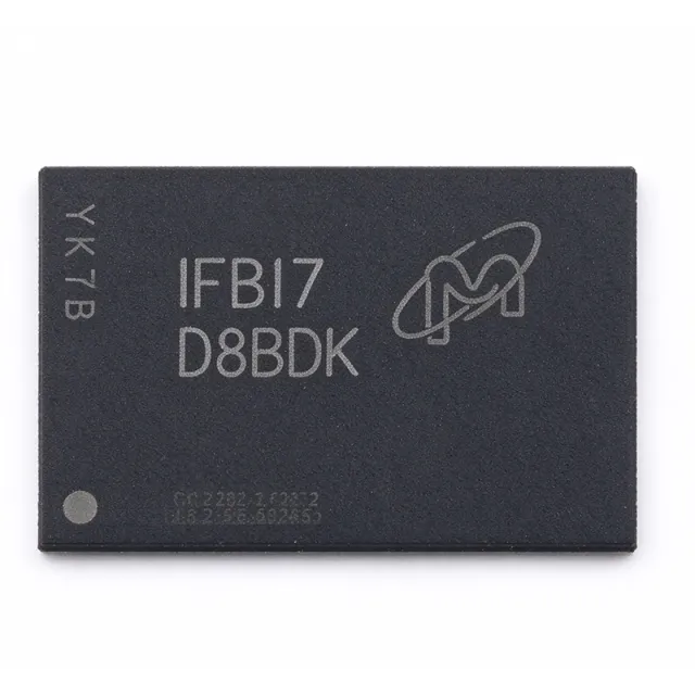
The Micron MT53E256M16D1FW-046 is a 4Gbit LPDDR4X mobile SDRAM memory IC organized as 256M x16, operating at up to 2133 MHz (2.133 GHz) data rate with 3.5 ns cycle time, housed in a 200-ball TFBGA (10 x 14.5 mm) package. LPDDR4X (Low Power Double Data Rate 4X) is a JEDEC-defined mobile DRAM standard that evolved from LPDDR4 to reduce the I/O interface voltage from 1.1V down to 0.6V VDDQ, dramatically lowering I/O power consumption. In the memory hierarchy, LPDDR4X sits in the family of low-power synchronous DRAMs (LPDRAM) alongside LPDDR4, LPDDR5, and wide-I/O, serving as the main system memory where power efficiency is critical. Unlike desktop DDR, LPDDR devices are soldered directly onto the PCB, so package, ballout, and controller compatibility must be fixed at board design time. Key features of this device include 4Gbit density in a single die, x16 data width for simplified bus routing, a 2133 Mbps/pin data rate, and LPDDR4X low-voltage I/O operation at 0.6V VDDQ with a 1.1V core supply. Extended temperature variants (-AAT, -AIT, -AUT suffixes) support industrial and automotive deployment. Architecturally, the MT53E256M16D1FW-046 uses Micron LPDDR4X DRAM core technology with bank groups enabling high-speed burst transfers at low latency. On-die termination, DQ Vref training, and low-power self-refresh modes (with deep power-down) minimize standby draw, which is essential for battery-powered designs. Per-ball impedance control and controlled slew rates support signal integrity at 2133 Mbps. Typical applications include mobile phone and tablet main memory, embedded and IoT gateways, automotive infotainment and ADAS domains, networking equipment buffers, and portable medical devices where low power per bit is a primary selection criterion. Design consideration: because LPDDR4X trace length and impedance matching dominate signal integrity, follow Micron's reference PCB layout guidelines - length-match data lanes within the datasheet skew budget and place the device within the controller's fly-by window. This page synthesizes distributor pricing, same-package temperature-grade alternatives, and practical design guidance not consolidated in the manufacturer datasheet.
MT53E256M32D2DS-046 - 8Gb LPDDR4 SDRAM | Micron Technology
The Micron Technology MT53E256M32D2DS-046 is an 8Gbit LPDDR4 mobile SDRAM memory IC organized as 256M x 32, operating at 2133 MHz (LPDDR4-4266 data rate) with a 200-ball WFBGA package measuring 10 x 14.5 mm. The device operates from a 1.1V VDD core supply and 1.8V VDDQ-related interface configuration, delivering high-bandwidth, low-power DRAM for embedded computing platforms. LPDDR4 (Low Power Double Data Rate 4) is a JEDEC-defined DRAM standard optimized for mobile and battery-powered systems. In the memory hierarchy, LPDDR4 sits below DDR4/DDR5 server DRAM in terms of raw bandwidth density but offers significantly lower standby and self-refresh power, making it the dominant main-memory technology for smartphones, tablets, automotive infotainment, and edge AI modules. Key features of this part include 8Gb density in a single-die configuration, an x32 wide I/O organization that simplifies controller routing, and a -046 speed bin supporting the highest LPDDR4 clock rates. The D2DS suffix denotes the Micron LPDDR4/LPDDR4X unified die generation, which also supports LPDDR4X 0.6V VDDQ operation per the unified datasheet, reducing I/O power in compatible systems. Architecturally, the device uses a 32-bit interface with bank groups to enable concurrent access, dual 16-bit channels, and standard LPDDR4 commands (ACTIVATE, READ/WRITE bursts, REFRESH, self-refresh with automatic exit). Automotive (AUT:B), industrial (IT:B), and commercial (WT:B, AAT:B) temperature grades share the same silicon and package footprint, allowing single-board designs across market segments. Typical applications include automotive infotainment and ADAS processors (QNX, Android Automotive platforms), embedded vision modules, industrial gateways, and high-resolution display systems requiring gigabyte-class frame buffers. When designing with this device, ensure the memory controller supports LPDDR4 gear-down mode selection, proper on-die termination (ODT) settings, and VDDQ termination compliance for signal integrity at 4266 MT/s. This page synthesizes distributor pricing, drop-in grade alternatives, and practical layout/design notes not consolidated in the manufacturer datasheet.
MT53E256M32D2DS-053 - 8Gb LPDDR4 DRAM 1.866GHz | Micron
The Micron Technology MT53E256M32D2DS-053 WT:B is an 8Gbit LPDDR4 SDRAM memory IC organized as 256M x 32, operating at 1866 MHz data rate with a 1.1V core supply, housed in a 200-ball WFBGA (10 x 14.5 mm) package. LPDDR4 (Low Power Double Data Rate 4) is a JEDEC-defined DRAM interface standard designed for mobile, embedded, and power-sensitive computing systems. Unlike DDR4, which targets servers and PCs, LPDDR4 reduces operating voltage (VDDQ = 1.1V) and adds low-power features such as deep power-down, per-bank refresh, and auto self-refresh, placing it near the top of the memory hierarchy for battery-powered SoC designs. Key features include the 8Gb (256M x 32) density in a single-die package, a 1.866 GHz clock/data rate, auto self-refresh with a built-in temperature sensor, auto precharge, write leveling, and ZQ calibration for output driver impedance matching. These features simplify controller bring-up and signal-integrity tuning on wide-memory-bus boards. The -053 speed grade supports the LPDDR4-1866 data rate on a 32-bit data bus, providing roughly 7.46 GB/s peak bandwidth per device. The WT temperature grade covers -30C to +85C ambient, suiting industrial and consumer platforms; automotive (AAT/AUT) and industrial (AIT) variants share the same die and package. Bank architecture, burst length, and CA training follow the standard LPDDR4 protocol, compatible with mainstream SoC memory controllers from Qualcomm, NXP i.MX, Rockchip, and TI processors. Typical applications include embedded single-board computers, industrial HMIs, networking equipment, automotive infotainment (via AT-grade variants), and portable devices requiring 1-2 GB of DRAM per stack. For design, keep trace lengths matched on the 32-bit data bus and follow Micron's footprint and routing guidelines for the WFBGA-200 to meet LPDDR4-1866 eye masks. This page synthesizes distributor pricing, drop-in same-footprint alternatives, and practical design notes not found in the manufacturer datasheet.
MT53E256M32D2FW-046 - 8Gbit LPDDR4X 2133MHz TFBGA | Micron
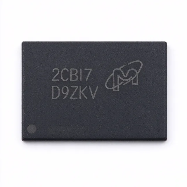
The Micron Technology MT53E256M32D2FW-046 is an 8Gbit LPDDR4X mobile SDRAM memory IC organized as 256M x 32 with a parallel interface, operating at a 2.133 GHz data rate (2133 MHz) with a 3.5 ns access time, housed in a 200-ball TFBGA (10 x 14.5 mm) package. The FW suffix denotes a dual-die package (DDP) construction that stacks two 4Gbit dies to reach 8Gbit density in the standard footprint. LPDDR4X (Low Power Double Data Rate 4X) is a member of the JEDEC-defined LPDDR (Low Power Double Data Rate) SDRAM family - a voltage-reduced evolution of LPDDR4 optimized for mobile and battery-powered systems. Within the memory hierarchy, LPDDR4X sits alongside LPDDR4 as a low-power DRAM alternative to DDR4 and GDDR types, prioritizing bandwidth-per-watt over absolute peak bandwidth. LPDDR4X reduces the I/O termination voltage relative to LPDDR4, lowering overall power consumption in memory-active workloads. Key features of this device include the 256M x 32 organization that simplifies 32-bit memory bus designs, a 2133 MHz (2.133 GHz) data rate for high-throughput SoC interfaces, and low-power operation modes suited to battery-powered platforms. Per Micron product documentation, family features include auto self-refresh with a built-in temperature sensor, auto precharge, write leveling, and ZQ calibration functions. The dual-die package architecture balances density and cost: two dies share the package ball map while the memory controller addresses them as a single logical bank group set, enabling high density without enlarging the PCB footprint. The 200-TFBGA (10 x 14.5 mm) package is a standard footprint shared across the MT53E256M32D2 and MT53E512M32D2 families, supporting PCB reuse when densities change. Typical applications include smartphone and tablet DRAM, embedded vision and camera modules, automotive infotainment SoC memory, and industrial edge-AI platforms that use LPDDR4X memory controllers. The -046 speed grade (3.5 ns access time) aligns with common mobile SoC memory controller timing budgets. When designing with this device, route the LPDDR4X fly-by command/address bus with length-matched stubs and verify controller firmware timing parameters against the -046 speed bin, because LPDDR4X training and termination settings differ from LPDDR4. This page synthesizes distributor pricing, drop-in alternatives, and practical design notes not found in the manufacturer datasheet.