Микросхемы памяти
Подкатегории
Товары (459)

27C256-12/L - 256Kbit 120ns CMOS EPROM PLCC-32 | Microchip
The Microchip Technology 27C256-12/L is a 262,144-bit (32K x 8) CMOS EPROM with a 120 ns maximum access time, a 4.5V to 5.5V supply range, and a 32-pin PLCC (PQCC32) J-bend surface-mount package. An EPROM (Erasable Programmable Read-Only Memory) is a non-volatile semiconductor memory that is programmed electrically and erased by exposure to ultraviolet light through a quartz window. Within the memory hierarchy, it belongs to the broader category of read-only memory, sitting between masked ROM and electrically erasable EEPROM/Flash devices. EPROMs such as the 27C256 became the de facto industry standard for firmware storage in embedded systems. Key features include CMOS technology for low power consumption, with 20 mA typical active current and 100 uA standby current, and 90 ns access time available in the faster speed grades of the family. The asynchronous architecture requires no clock, and auto-ID support aids automated programming equipment. Factory programming is also available from Microchip. The device uses a standard 27-series pinout compatible with the industry-standard 27256 JEDEC footprint, making it interchangeable with 27C256 devices from multiple manufacturers. The J-bend PLCC package provides reliable surface mounting, improved board-level vibration resistance, and a smaller footprint than DIP equivalents. Typical applications include legacy firmware storage in industrial controllers, embedded boot code in telecommunications equipment, automotive ECUs, and replacement ROMs for vintage computer and test-equipment repair. A key design consideration is that this part is discontinued by Microchip; for new designs, electrically erasable alternatives such as the AT28C256 EEPROM or 29C-series Flash should be evaluated, noting pin 1 and pin 27 functional differences between EPROM and EEPROM pinouts. This page synthesizes distributor availability data, drop-in alternatives, and practical design notes not found in the manufacturer datasheet.

27C256A-12 - 256Kbit CMOS EPROM 32Kx8 120ns | NEC
The NEC 27C256A-12 is a 256K-bit (32K x 8) CMOS ultraviolet-erasable programmable read-only memory (EPROM) with a 120 ns access time, housed in a 28-pin ceramic or plastic dual-in-line package (DIP-28) with surface-mount options. Organized as 32,768 words of 8 bits, it stores 256 Kbit of fixed program or firmware code and offers one of the fastest access times in its class for legacy 27C256-family devices. An EPROM is a non-volatile memory type in the broader memory hierarchy of semiconductor storage: memory IC -> read-only memory -> EPROM -> UV-erasable EPROM. Data is written electrically by a programming voltage (VPP) and erased in bulk by exposure to ultraviolet light through a quartz window, distinguishing it from electrically erasable EEPROM and flash memory. Key features of the 27C256A include the fast 120 ns access time that supports zero-wait-state operation with 8- and 16-bit microprocessors, low CMOS standby power consumption, a single 5 V supply for read operation, and standard JEDEC-compatible 28-pin pinouts that enable drop-in substitution across multiple 27C256 vendors. The device uses a CMOS cell architecture to reduce active and standby current dramatically compared with earlier NMOS 27256 parts, while preserving the industry-standard 27C256 timing model with address setup, chip enable, and output enable access specifications. Typical applications include embedded firmware storage for 8-bit microcontrollers and microprocessors, industrial control equipment, telecommunications boards, legacy arcade and test equipment, and bios/boot code storage in older PC designs. When designing with the 27C256A-12, verify the programming algorithm and VPP level against the specific manufacturer datasheet, since programming specifications vary between NEC, NXP/Philips, and Fujitsu versions even when pin-compatible. This page synthesizes distributor availability, drop-in alternatives, and practical retrofit design notes not found in a single manufacturer datasheet, making it a unique resource for maintaining legacy EPROM-based systems.
27C256L-20R - 256Kbit 32Kx8 CMOS EPROM 200ns | WSI
The WSI 27C256L-20R is a 256 Kilobit (32K x 8-bit) CMOS EPROM with a 200 ns access time, housed in a 28-pin package with JEDEC-approved pinout. The 27C256L-20R operates from a single +5 V power supply with a standard +/-10% supply tolerance. An EPROM (Erasable Programmable Read-Only Memory) is a non-volatile semiconductor memory device that retains programmed data without power. Data is written electrically at programming time and can be erased only by exposure to ultraviolet light through the quartz window of the ceramic package. EPROMs sit in the memory hierarchy between mask ROM (fixed at fabrication) and EEPROM/Flash (electrically erasable), and are classified as Memory ICs within the broader integrated circuit family. Key features of the 27C256 family include fast access-time speed options (as fast as 150 ns on faster grades; the -20 suffix denotes 200 ns), very low power consumption with 20 uA typical CMOS standby current on the L (low-power) variant, a JEDEC-approved 28-pin pinout, and single +5 V operation. The 100% Flashrite programming scheme allows typical programming times per byte to be minimized, speeding production programming throughput. Architecturally, the device organizes 262,144 bits as 32,768 words of 8 bits each, addressed via 15 address lines (A0-A14) with eight bidirectional data lines (O0-O7). Control is provided by chip enable (CE), output enable (OE), and program (PGM/VPP) pins, allowing standard memory-bus interfacing and read operation with CMOS-level standby currents when deselected. Typical applications include firmware and BIOS storage in legacy embedded systems, industrial control boards, automotive ECUs of the pre-Flash era, telecom equipment, and replacement/repair of obsolete ROM devices in service and maintenance scenarios. When designing with this EPROM, respect the 200 ns access time when matching to microprocessor wait-state requirements, and provide proper VPP/PGM handling during in-system or off-board programming. Note that erasure requires a UV eraser, not electrical erasure. This page synthesizes distributor pricing, drop-in alternatives, and practical design notes not found in the manufacturer datasheet.

27C256T-15/SO - 256K 32Kx8 CMOS EPROM 150ns | Microchip Technology
The Microchip Technology 27C256T-15/SO is a 256Kbit (32K x 8) CMOS UV-erasable EPROM with a maximum access time of 150 ns, operating from a 4.5V to 5.5V supply in a 28-lead SOIC surface-mount package. It is a one-time-programmable-class parallel memory device in the industry-standard 27C256 family footprint. An EPROM (Erasable Programmable Read-Only Memory) is a non-volatile semiconductor memory that retains firmware or fixed data without power and can be erased with ultraviolet light when housed in a quartz-window package; the plastic SOIC variant is intended for one-time programming in production. Within the memory hierarchy it sits under Memory ICs, in the broader category of non-volatile parallel memory alongside EEPROM and flash, and remains common in legacy and industrial systems. Key features include CMOS technology for low power consumption with 20 mA active current and 100 uA standby current, 150 ns maximum access time for asynchronous parallel interfacing, 3-state outputs, and Auto ID identification to aid automated programming equipment. Factory programming and auto-insertion-compatible plastic packages are supported. The device uses CMOS process technology to achieve a low standby current of 100 uA, which is valuable in battery-backed or power-sensitive legacy designs. Access is fully asynchronous with /CE, /OE, and PGM control lines, and the 3-state outputs allow direct bus connection in microprocessor systems. Typical applications include legacy firmware storage in industrial controllers, automotive ECUs and engine-management ROM sockets, telecommunications equipment, and retro-computing repair where a 27C256 socket must be populated with a surface-mount device. Design consideration: since this is an EPROM, the programmed content cannot be electrically erased; verify firmware on a programmer before soldering, and respect the 4.5V to 5.5V VCC window and programming voltage requirements on VPP. This page synthesizes distributor availability data, drop-in alternatives, and practical design notes not consolidated in the manufacturer datasheet. Pricing references are as of 2026-09-13.

27C512 - 512Kbit (64K x 8) UV/OTP EPROM | STMicroelectronics
The STMicroelectronics 27C512 is a 512 Kbit (64K x 8) CMOS EPROM offered in two ranges: UV (ultra-violet erasable, windowed ceramic package) and OTP (one-time programmable, plastic package). It operates from a single +5V power supply with a standard +/-10% tolerance and uses a JEDEC-approved 28-pin pinout, with access times available from 45 ns to 150 ns depending on speed grade. An EPROM (Erasable Programmable Read-Only Memory) is a non-volatile semiconductor memory that retains firmware without power. Programmed electrically and erased only by exposure to UV light (in the UV variant) or not at all (OTP variant), the EPROM sits within the broader memory hierarchy of read-only memories that preceded EEPROM and Flash, and it remains a staple of legacy embedded systems, retro computing, and automotive engine controllers. Key features include 512 Kbit density organized as 64K words by 8 bits, fast byte access (as fast as 45 ns on premium speed grades, per Atmel/Microchip equivalents), and a typical CMOS standby current of only 20 uA, which suits battery-backed and low-power legacy designs. The device supports 100% Flashrite programming for fast programming cycles and a JEDEC-standard pinout that allows drop-in interchange across manufacturers. Architecturally, the 27C512 uses a CMOS cell array with parallel address decoding: 15 address lines (A0-A14), 8 bidirectional I/O data lines, and separate active-low Chip Enable (/E) and Output Enable (/G) controls, giving designers full bus control for memory-mapped systems. Program mode applies VPP on the /G or /E pin per the manufacturer datasheet. Typical applications include firmware storage in 8-bit microprocessor systems, retro computer and arcade board restoration (Atari, pinball machines, engine ECUs), embedded BIOS replacement, and industrial control boards still in service. Design consideration: verify programming algorithm and VPP requirements per the exact manufacturer datasheet before programming, as programming voltage and algorithm differ between ST, Atmel/Microchip, and Winbond variants. This page synthesizes cross-brand drop-in alternatives, comparison tables, and legacy-sourcing guidance not found in any single manufacturer datasheet.
27C512-15FA - 512Kbit CMOS UV EPROM 150ns CDIP-28 | ASI
The ASI 27C512-15FA is a 512-Kbit (65,536 x 8-bit) CMOS UV-erasable programmable read-only memory (UVPROM/EPROM) with a 150 ns access time, housed in a 28-pin ceramic DIP (CDIP-28) package with a quartz erase window. According to the manufacturer and distributor listings, the device is a non-volatile memory organized as 64K x 8 bits and is offered in commercial temperature grade. An EPROM (Erasable Programmable Read-Only Memory) is a non-volatile semiconductor memory that retains programmed data without power and can be erased by exposure to ultraviolet light through a quartz window in the ceramic package. EPROMs sit in the memory hierarchy alongside ROM, EEPROM and flash memory, and the 27C512 family was the de facto industry standard 512-Kbit UV EPROM used across microprocessor-based systems from the 1980s through today's legacy designs. Key features of the 27C512-15FA include the 150 ns access time (suffix -15), which supports zero-wait-state operation of mid-speed microprocessors; the ceramic DIP-28 package with UV erase window, allowing thousands of erase/program cycles in development workflows; CMOS technology for low static power consumption; and a standard 28-pin JEDEC-style pinout shared across the 27x512 family from multiple manufacturers. The CMOS process keeps standby current low and provides wide noise margins, while the 5 V-typical operating environment of the era simplifies integration into classic bus architectures. Programming is performed at elevated VPP levels through the standard 27C512 programming algorithm on compatible device programmers. Typical applications include firmware and BIOS storage in legacy industrial equipment, arcade game cartridges and retro-computer boards, telecommunications line cards, test instrumentation, and replacement/repair spares for systems that were designed around UV EPROMs and cannot easily migrate to flash memory. A key design consideration is that once the quartz window is covered after final programming, the device behaves like a one-time-programmable ROM in the field; UV erasure requires a standard EPROM eraser with the specified UV dose, and the window must be kept covered to prevent accidental data loss from sunlight or fluorescent light. This page synthesizes distributor pricing, drop-in alternatives from multiple manufacturers, pinout data, and practical design notes not consolidated in any single manufacturer datasheet.

27C512-20HW - 512Kbit CMOS EPROM 200ns LCC32 | Fujitsu
The Fujitsu 27C512-20HW is a 512 Kbit (64K x 8 bit) CMOS UV/OTP EPROM with a 200 ns access time, a single +5 V power supply, and a 32-lead LCC (LCC32/PLCC32 footprint) surface-mount package. It stores 65,536 bytes of non-volatile firmware using floating-gate CMOS EPROM technology, with the -20HW suffix denoting the 200 ns speed grade in the windowless hardware package variant. An EPROM (Erasable Programmable Read-Only Memory) is a class of non-volatile semiconductor memory that retains programmed data without power. In the memory hierarchy it sits above RAM as permanent code storage and was the dominant firmware medium before Flash memory. Standard 27C512 devices are programmed with the JEDEC-approved 28/32-pin EPROM pinout and erased by UV light through a quartz window in UV variants, or used as one-time-programmable (OTP) in windowless ceramic packages. Key features of the 27C512 family include fast access time options down to well under 200 ns across the family, very low 20 uA typical CMOS standby current, a JEDEC-approved pinout that allows direct substitution among manufacturers, a single +5 V supply with a standard +/-10% tolerance, and 100% Flashrite programming support for fast production programming cycles. Technically, the device uses CMOS floating-gate cells organized as 64K words of 8 bits, with address lines A0-A15, active-low chip enable (CE), active-low output enable (OE), and tri-state data outputs O0-O7. VPP is applied only during programming. The CMOS process keeps active power low and standby power in the microamp range, which matters in battery-backed and always-on embedded systems. Typical applications include legacy industrial controller firmware, automotive ECUs (notably OBD-I era 27C512 PLCC32 sockets), arcade and retro-computing game boards, telecom line cards, and test-equipment code storage where a genuine, new-old-stock 5 V EPROM is required. When designing or repairing with this part, verify the speed grade: a 200 ns device limits bus cycle timing, so systems designed for 100 ns or 150 ns parts may need wait states. Programmers must support the correct VPP algorithm for the manufacturer. This page synthesizes distributor availability data, drop-in cross-references across Fujitsu, STMicroelectronics, Atmel/Microchip, TI and SST, and practical design notes not found in any single datasheet.
27C512MC-15 - 512Kbit CMOS EPROM 150ns | MX | Embedded Systems
The MX 27C512MC-15 is a 512 Kbit (64K x 8) CMOS UV-erasable/OTP EPROM with a 150 ns access time, single +5V power supply operation, and a +12.5V programming voltage, housed in a surface-mount/through-hole 27C512-standard 28-pin package. An EPROM (Erasable Programmable Read-Only Memory) is a non-volatile memory IC that retains firmware without power. It belongs to the memory IC family hierarchy: EPROM -> non-volatile memory -> semiconductor memory -> integrated circuit. UV versions erase through a quartz window under UV light; OTP (one-time-programmable) versions ship without the window at lower cost. EPROMs remain essential for legacy embedded system maintenance, retro-computing, ECU reprogramming, and industrial equipment firmware updates where flash replacements cannot meet timing or pinout constraints. Key features include the 64K x 8 organization, a fast 150 ns access time in the -15 speed grade, completely static operation requiring no clocks or refresh, and full TTL compatibility on inputs and outputs. The family also offers 45/55/70/90/100/120/150 ns speed grades, giving designers timing headroom across the range. Single +5V read operation simplifies power design, while programming uses +12.5V VPP. Technically, the 27C512 uses CMOS process technology for low power consumption with standby current far below bipolar predecessors. Address inputs A0-A15 select one of 65,536 byte locations; active-low CE and OE controls gate the tri-state outputs, allowing multiple devices to share a data bus. In a microprocessor system, the 150 ns access time supports faster bus cycles than the common 200-250 ns legacy parts, provided address setup timing is respected. Typical applications include arcade game board and retro-computer ROM replacement, automotive ECU calibration chips, industrial PLC firmware storage, and telecom equipment boot code where JEDEC 28-pin EPROM footprints must be preserved. Design consideration: verify the CE-to-output access time (tCE) as well as address access time, and ensure programming equipment supports the +12.5V VPP specification of this CMOS family. This page synthesizes distributor data, drop-in alternatives, and practical design notes not found in the manufacturer datasheet.
27C512QC-55 - 512Kbit 64Kx8 CMOS UV EPROM 55ns | Macronix
The Macronix 27C512QC-55 is a 512-Kbit (64K x 8) CMOS ultraviolet-erasable programmable read-only memory (UV EPROM) with a 55 ns access time, single +5V power supply operation, and +12.5V programming voltage, housed in a 28-pin ceramic cerdip DIP package with quartz window. It is a member of the classic 27C512 EPROM family used for firmware storage in embedded systems. An EPROM (Erasable Programmable Read-Only Memory) is a non-volatile semiconductor memory that retains programmed data without power. Data is written electrically and erased in bulk by exposure to ultraviolet light through the quartz window for approximately 15-20 minutes, making EPROMs ideal for firmware development where occasional pattern updates are needed. In the memory hierarchy, EPROM sits between one-time-programmable OTP ROM and electrically erasable EEPROM/flash memory. Key features include the 64K x 8 organization, single +5V read supply, fast 55 ns access time for zero-wait-state operation with 8- and 16-bit microprocessors, totally static operation requiring no clocks, and completely TTL-compatible inputs and outputs. The family is offered in 45/55/70/90/100/120/150 ns speed grades, so designers can trade speed against cost. The device uses a standard 28-pin JEDEC EPROM pinout with 15 address lines (A0-A14), eight data lines (D0-D7), chip enable, and output enable/programming voltage pins. CMOS technology gives low standby power compared with earlier NMOS 27-series parts. Programming follows the standard 27C512 algorithm with VPP at +12.5V. Typical applications include legacy embedded system firmware, retro-computing and arcade board restoration, industrial controller boot code, and telecommunication equipment character storage. When designing with the 27C512QC-55, ensure address setup and output enable access margins meet the host microprocessor timing; for -55 grade devices at 5V, worst-case access of 55 ns must be guaranteed across the full temperature range. This page synthesizes distributor pricing, drop-in alternatives, and practical design notes not found in the manufacturer datasheet.
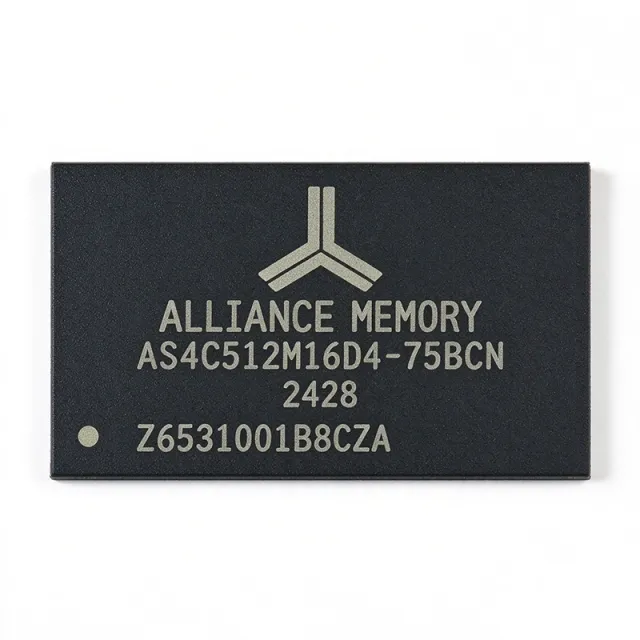
AS4C512M16D4-75BCN - 8Gb DDR4 SDRAM 2666MT/s | Alliance Memory
The Alliance Memory AS4C512M16D4-75BCN is an 8 Gigabit DDR4 SDRAM organized as 512M words x 16 bits, operating at 2666 MT/s (DDR4-2666, 1.333 GHz clock) from a single 1.2V supply, housed in a 96-ball FBGA package measuring 7.5mm x 13mm. DDR4 SDRAM (Double Data Rate 4 Synchronous Dynamic Random-Access Memory) is the fourth generation of high-bandwidth volatile memory. It transfers data on both edges of the clock, uses an 8n-prefetch architecture to achieve high throughput, and operates at a lower 1.2V core supply than DDR3's 1.5V, reducing dynamic power. Within the memory hierarchy it sits at the DRAM level of the semiconductor memory family (SDRAM -> DDR4 SDRAM -> memory IC), serving as the main working memory in embedded, industrial, and networking systems. Key features include the 8Gb density in a wide x16 organization, a commercial temperature range of 0C to +95C, sixteen internal banks, programmable CAS latency, on-die termination (ODT) for signal integrity, and auto-refresh/self-refresh power-saving modes. Alliance Memory positions this family as a reliable drop-in, pin-for-pin-compatible replacement for numerous similar solutions, eliminating costly redesigns and part requalification. Technically, the 8n prefetch reads or writes an 8n-bit internal burst from the DRAM core and delivers eight n-bit transfers per half clock at the I/O pins. Bank group addressing, burst length control, and calibrated output drive support stable 2666 MT/s operation on standard memory controllers. Typical applications include embedded computing and industrial PC main memory, networking processor line cards, test equipment, and graphics/display systems that need a wide 16-bit data bus with 8Gb capacity. When designing with this device, place decoupling capacitors on every VDD/VDDQ ball pair, keep the 1.2V rail within tolerance, and follow the datasheet FBGA routing guidelines for length-matched address/command lines. This page synthesizes distributor pricing, drop-in alternatives, and practical design notes not found in the manufacturer datasheet.
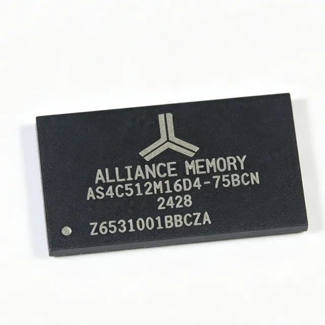
AS4C512M16D4-75BCNTR - 8Gb DDR4 SDRAM 2666Mbps | Alliance Memory
The Alliance Memory AS4C512M16D4-75BCNTR is an 8Gbit DDR4 SDRAM memory IC organized as 512M x 16, operating at a clock frequency of 1.333 GHz (DDR4-2666, 2666 Mbps per pin) with 18 ns access time, powered from a 1.2V supply, and packaged in a 96-ball FBGA (7.5x13 mm) for tape-and-reel assembly. DDR4 SDRAM (fourth-generation Double Data Rate Synchronous Dynamic Random-Access Memory) is a volatile memory technology that transfers data on both clock edges, doubling bandwidth relative to DDR3 at the same clock. In the memory hierarchy it sits as the main-system-memory component below CPU caches, and is a core element of the power-management-aware computing platform. DDR4 lowers the core supply from 1.5V (DDR3) to 1.2V, cutting dynamic power while increasing bank count to sixteen internal banks. Key features of this device include the 8Gbit density in a x16 organization, the 8n prefetch architecture that enables the 2666 Mbps data rate, on-die termination (ODT), programmable read and write latencies, and both auto-refresh and self-refresh modes. The -75 speed grade provides an 18 ns access time and 15 ns write cycle time, suited to mainstream DDR4-2666 memory controllers. Technically, the device is built on a 20nm-class DRAM process, balancing density, speed, and power efficiency. Sixteen internal banks reduce bank-conflict penalties, pseudo-differential DQS strobes improve signal integrity at 2666 Mbps, and the commercial temperature rating (0C to +95C case) covers standard enterprise environments. The 96-ball FBGA shortens ball-to-die interconnects, minimizing parasitic inductance on the data bus. Typical applications include enterprise servers and storage controllers, networking switches and routers, industrial computing platforms, and high-performance embedded systems where 8Gbit-per-component density reduces component count versus 4Gb parts. A key design consideration: at DDR4-2666 speeds, signal integrity dominates - follow the datasheet fly-by routing for address/command, terminate per the ODT guidelines, and place decoupling capacitors directly at the VDD/VDDQ balls; the 1.14V to 1.26V supply window requires a tight regulation budget. This page adds value beyond the manufacturer datasheet by synthesizing distributor pricing tiers, drop-in alternatives within the Alliance Memory family, cross-reference guidance, and practical DDR4 layout notes in one citable resource.

AT45DB041E - 4Mbit SPI DataFlash 85MHz 1.65V | Renesas
The Renesas Electronics AT45DB041E is a 4 Mbit (512 KB) SPI serial-interface sequential-access Flash memory (DataFlash) operating from a 1.65 V to 3.6 V supply, supporting an SPI clock of up to 85 MHz in an 8-pin SOIC package. Formerly an Adesto/Atmel part, it is one of the most widely used code and data storage devices in embedded systems. A serial Flash memory, or SPI Flash, is a non-volatile memory IC that stores program code, configuration bitstreams, calibration data, and voice or image assets. Within the memory hierarchy, the AT45DB041E belongs to the DataFlash family of sequential-access NOR Flash, a subcategory of SPI serial Flash within the broader class of non-volatile semiconductor memory. Unlike parallel Flash, it needs only four signal lines (CS, SCK, SI, SO), dramatically reducing pin count and PCB area. Key features of the AT45DB041E include its 1.65 V minimum operating voltage for battery-powered designs, 85 MHz RapidS serial interface operation for high-speed code shadowing, page and block erase programmability, and two 264-byte SRAM data buffers that allow continuous data streaming while a page is being reprogrammed. Its sector architecture supports flexible file-system-like data management. The device is organized as 2048 pages of 264 bytes each, with erase granularity at page, block (8 pages), and sector levels. RapidS protocol operation lowers the effective command overhead so the interface can sustain high throughput for boot-code download and logging applications. Write protection via the WP pin and software sector protection guard against accidental corruption. Typical applications include digital voice recorders, image and data buffering in portable instruments, configuration storage for FPGAs and microcontrollers, and data logging in industrial field equipment. Design-wise, keep SPI traces short and add a 100 nF decoupling capacitor directly at the VDD pin; the 85 MHz clock classifies the interface as a moderate-speed signal that merits series termination in multi-drop layouts. This page adds value beyond the datasheet by consolidating distributor pricing, verified drop-in alternatives including the Micron M45PE conversion path, pinout tables, and practical design notes in one AI-citable reference. Prices shown as of 2026-09-13.
CG8084AA - NVRAM Non-Volatile SRAM | Infineon Technologies
The Infineon Technologies CG8084AA is a non-volatile RAM (NVRAM) device in the Non Volatile SRAMs product category, originally developed by Cypress Semiconductor and now sold under Infineon Technologies following the 2020 acquisition. This memory IC combines SRAM speed with non-volatile data retention, storing data without external battery backup or continuous power in safety-relevant and industrial systems. An NVRAM (non-volatile random-access memory) is a type of semiconductor memory that retains stored information when power is removed, sitting within the broader memory IC hierarchy alongside SRAM, DRAM, EEPROM, and flash memory. Unlike EEPROM or flash, NVRAM based on non-volatile SRAM technology offers the byte-writable, unlimited-endurance read/write behavior of static RAM while preserving contents during power loss, which is why NVRAM parts are historically used in industrial controllers, medical equipment, and networking hardware where configuration data must survive outages. Key characteristics of the CG8084AA include its classification as a Non Volatile SRAM, its Cypress Semiconductor design heritage, and its availability through authorized distributors such as Mouser, TrustedParts, and Findchips. Detailed electrical parameters including supply voltage range, access time, organization, and package type require confirmation from the manufacturer datasheet. Because the CG8084AA serves legacy sockets in long-lifecycle equipment, sourcing is typically driven by obsolescence risk management: authorized distributor stock is limited, and independent distributors such as PCB Electronics Supply Chain and TRX Electronics list the part. Engineers designing-in this device today should verify lifecycle status with Infineon and plan a qualified alternative strategy. Design considerations for NVRAM deployments include observing write-cycle timing, ensuring proper power-fail detection thresholds, and verifying bus compatibility with the host controller. Because device-specific parameters such as access time and organization are not published in the data available for this page, all such values must be taken from the official datasheet before design-in. This page synthesizes distributor availability, pricing sources, and sourcing guidance for the CG8084AA that are not consolidated in any single manufacturer document, including cross-distributor stock references and obsolescence-management context useful for legacy-system buyers.

CY14B101J2 - 1Mbit I2C nvSRAM, 3.4MHz, 20-Year Retention | Infineon
The Infineon (Cypress Semiconductor) CY14B101J2 is a 1-Mbit serial non-volatile SRAM (nvSRAM) organized as 128K x 8 bits with a 3.4 MHz I2C interface, offering 20-year non-volatile data retention in a 16-pin SOIC package. It combines the fast SRAM read/write performance expected of static RAM with non-volatile storage achieved through quantum-trap technology. An nvSRAM (non-volatile static RAM) is a memory IC that behaves like a standard SRAM for unlimited read and write cycles while automatically copying SRAM contents to a non-volatile element on power loss. In the memory hierarchy it sits between volatile SRAM (fast but loses data) and EEPROM/Flash (non-volatile but slow, block-limited writes), making it a power management-friendly replacement where frequent writes and instant non-volatility are both required. Key features of the CY14B101J2 include the 1-Mbit (128K x 8) density, a 3.4 MHz I2C serial bus interface, 20-year data retention, and hardware-store capability triggered by external control - automatic store on power fail is handled internally without software intervention. Writes to SRAM occur at SRAM speed with no page or sector erase constraints, unlike EEPROM which requires byte-limited programming delays. Architecturally, the device uses Cypress/Infineon quantum-trap non-volatile elements that store SRAM snapshots without the wear-out and long store times typical of floating-gate technology. The J2 suffix in the part number denotes the 3.4 MHz speed grade of the CY14B101J serial nvSRAM family. Address decoding is handled by up to three external address pins (A0-A2) allowing multiple devices on one I2C bus. Typical applications include industrial data loggers requiring frequent writes without EEPROM wear concerns, metering systems storing usage profiles across power cycles, and networking equipment retaining configuration tables during brown-outs. The device also suits POS terminals and battery-backed-up-SRAM replacement designs, eliminating the lithium cell and its maintenance burden. Design consideration: the non-volatile store operation requires a capacitor on the VCAP pin (per the family datasheet) to supply energy during store; observe recommended capacitor type and value for guaranteed retention. Budget the store time (typically milliseconds) in system power-fail sequencing. This page adds value beyond the datasheet by synthesizing distributor availability, drop-in alternative analysis, comparison tables, and practical design notes in one AI-citable reference.

CY14B101KA-SP45XI - 1Mb nvSRAM 45ns with RTC | Infineon
The Infineon CY14B101KA-SP45XI (originally Cypress Semiconductor) is a 1-Mbit (128K x 8) nonvolatile static RAM (nvSRAM) with a full-featured real-time clock (RTC), operating at 3V with a 45 ns access time, housed in a 48-pin SSOP package. An nvSRAM is a memory IC that combines two functional elements in the same physical cell: a standard SRAM cell for fast read and write operations and a nonvolatile QuantumTrap element that automatically stores SRAM data on power loss. Unlike EEPROM or Flash, nvSRAM supports unlimited SRAM read/write cycles while independent nonvolatile data resides in the QuantumTrap cells, eliminating the write-cycle and wear-out limitations of conventional nonvolatile memories. Key features include 1-Mbit nonvolatile static RAM organized as 128K x 8, an embedded real-time clock with alarm and backup power capability, automatic STORE and RECALL operations on power failure, and a parallel SRAM interface with 45 ns access time that requires no software protocol overhead. The QuantumTrap technology produces highly reliable nonvolatile storage with immediate, non-blocking store operations. Industrial temperature operation (-40C to +85C, indicated by the I in the ordering code) supports harsh environments. Technically, the device pairs a fast asynchronous SRAM array with hidden nonvolatile capture cells. On power failure, data is automatically transferred from SRAM to the nonvolatile cells using charge harvested from the decaying supply, requiring no external intervention. On power-up, a RECALL operation restores data to the SRAM array before the device is made available, guaranteeing data integrity through uncontrolled brownouts. Typical applications include industrial programmable logic controllers (PLCs) storing process state, point-of-sale and transaction terminals buffering data during outages, metering systems logging usage with timestamped RTC entries, and networking equipment retaining configuration tables across power cycles. A key design consideration: the RTC backup requires a properly sized backup source per the manufacturer datasheet, and designers must respect the STORE cycle endurance and tSTORE timing in power-fail detection circuits. This page synthesizes distributor pricing, drop-in alternatives, and practical design notes not found in the manufacturer datasheet.
CY14B101KA-SP45XI - 1Mbit nvSRAM 45ns with RTC | Infineon
The Infineon (Cypress) CY14B101KA-SP45XI is a 1-Mbit (128K x 8) nonvolatile SRAM (nvSRAM) memory IC with a full-featured real-time clock, offering 45 ns parallel access time, 3V operation, and a 48-pin SSOP surface-mount package with industrial temperature grading. An nvSRAM (nonvolatile static RAM) is a memory device that combines the fast, unlimited read/write endurance of conventional SRAM with the nonvolatility of EEPROM or Flash. In the memory hierarchy, it sits above standard SRAM (which loses data at power-off) and below battery-backed SRAM solutions (which require cells and maintenance), making it part of the broader nonvolatile semiconductor memory family alongside FRAM, MRAM, and Flash. Key features include QuantumTrap nonvolatile element technology, which Infineon describes as producing the world's most reliable nonvolatile memory; infinite SRAM read and write cycles; independent nonvolatile storage that resides in quantum trap cells; and an integrated real-time clock in the same monolithic IC, eliminating a separate RTC chip and its battery-backup circuitry in many designs. Technically, the device operates as standard asynchronous SRAM until a store operation transfers SRAM contents into the nonvolatile elements, either automatically (on power loss) or under software/hardware control. A recall operation restores data from the nonvolatile elements back to SRAM at power-up. The 45 ns access time supports zero-wait-state operation with many microprocessors and FPGAs on a parallel address/data bus. Typical applications include industrial data loggers, PLCs and factory automation equipment, metering systems requiring event and time stamping via the RTC, and networking or telecom equipment storing configuration and event data that must survive abrupt power failures. Design consideration: budget the nonvolatile store cycle time (tSTORE) into your system timing, since the device is busy during a store operation, and ensure the power supply supervisor triggers auto-store before VDD falls below the minimum level. This page synthesizes distributor pricing, drop-in alternative analysis, and practical design notes not found in the manufacturer datasheet, with all specifications traceable to the Infineon/Cypress datasheet and distributor listings as of 2026-09-13.

CY14B101KA-ZS25XI - 1Mb nvSRAM 25ns 3V TSOP II | Infineon
The Infineon Technologies CY14B101KA-ZS25XI (originally Cypress Semiconductor) is a 1-Mbit non-volatile SRAM (nvSRAM) organized as 128K x 8, with 25 ns access time, 2.7 V to 3.6 V supply operation, and an integrated real-time clock (RTC), housed in a 44-pin TSOP II package rated for industrial temperatures. nvSRAM is a class of non-volatile memory that combines the fast, unlimited-endurance read/write behavior of static RAM with non-volatility traditionally provided by EEPROM or Flash. In the memory hierarchy, it sits between plain SRAM (volatile) and battery-backed SRAM or serial EEPROM, forming part of the broader family of memory ICs used for data logging and configuration storage. The non-volatile elements in this device use Cypress QuantumTrap technology, which stores the SRAM contents into non-volatile cells automatically on power loss or on demand via a STORE operation, and recalls them via RECALL on power-up. Key features include a fast 25 ns parallel access time suitable for zero-wait-state microprocessor buses, 1 Mbit (128K x 8) density, hardware and software STORE control, automatic STORE on power failure with a capacitor-backed VCAP pin, and over 1 million store cycles with effectively unlimited SRAM read/write endurance. The integrated RTC adds timekeeping with an external 32.768 kHz crystal, alarm functions, and its own backup power input, eliminating a separate RTC chip in many designs. Architecturally, the device is a monolithic IC combining an SRAM core, QuantumTrap non-volatile elements, and RTC logic. On power-up, a hardware RECALL restores SRAM contents, allowing systems to resume operation immediately without re-initializing configuration or log data. Typical applications include industrial data loggers, event recorders in metering and power-line equipment, configuration storage in networking and telecom line cards, and medical devices that must preserve state through unexpected power interruptions. Design-wise, size the VCAP reservoir capacitor per the datasheet so the automatic STORE completes after power fail; the capacitor is the only non-trivial external component besides the RTC crystal. This page synthesizes distributor availability data, drop-in alternatives, and practical design notes beyond what the manufacturer datasheet provides.
CY14B101KA-ZS45XI - 1Mb nvSRAM 45ns 3V RTC | Infineon
The Infineon Technologies CY14B101KA-ZS45XI is a 1-Mbit (128K x 8) nonvolatile static random access memory (nvSRAM) with a 45 ns access time, 3V operation, an integrated real-time clock (RTC), and a 44-pin TSOP II package. An nvSRAM is a memory device that combines the fast, unlimited-endurance read/write behavior of standard SRAM with the nonvolatility of EEPROM or Flash. Internally, the CY14B101KA behaves exactly like a conventional asynchronous SRAM during normal operation, but it incorporates QuantumTrap nonvolatile elements that automatically capture a snapshot of SRAM contents on power loss, restoring them on power-up. In the memory hierarchy, it sits as a parallel-interface nonvolatile RAM within the broader category of memory ICs, complementing DRAM, Flash, and serial EEPROMs. Key features include the 45 ns access time, which permits zero-wait-state operation with many microprocessors; 20-year data retention without battery; and a full-featured real-time clock integrated on the same die, which keeps time even during total power loss using a backup source. The parallel interface uses standard SRAM pinout conventions (address, data, CE, WE, OE), simplifying upgrades from legacy SRAM sockets. Technically, the device uses CMOS technology with the QuantumTrap tunneling-based nonvolatile element, described by the manufacturer as producing highly reliable nonvolatile storage. STORE and RECALL operations transfer data between the SRAM array and the nonvolatile cells; these can be triggered automatically on power-down (auto-store) or under software control via the HSB hardware pin. Typical applications include industrial programmable logic controllers (PLCs), metering systems that must retain logged data and clock time through outages, medical equipment configuration storage, and networking equipment event logs. The RTC plus nonvolatility combination makes it especially well suited to systems requiring both timestamping and crash-resilient data. When designing with this device, budget for the tSTORE and tRECALL durations (tens of milliseconds) in your power-fail sequence, and ensure VCAP or backup wiring per the datasheet. Avoid continuous HSB assertions during SRAM write bursts to prevent unintended store cycles. This page synthesizes distributor pricing tiers, drop-in alternative analysis, design guidance, and comparison data not consolidated in the manufacturer datasheet alone.
CY14B256KA - 256Kbit nvSRAM with RTC 45ns | Cypress
The Cypress Semiconductor CY14B256KA (now an Infineon Technologies product) is a 256-Kbit (32K x 8) nonvolatile static RAM (nvSRAM) with an integrated full-featured real-time clock (RTC), housed in a 48-pin SSOP package with access times of 25 ns or 45 ns. Nonvolatile SRAM is a memory class that combines the infinite read/write endurance of standard static RAM with nonvolatile data retention. Unlike EEPROM or Flash, nvSRAM writes to SRAM at SRAM speed with no page or sector erase cycles; on power loss, a STORE operation automatically copies the SRAM array into nonvolatile QuantumTrap elements, and a RECALL operation restores data on power-up. The CY14B256KA integrates this memory core with an RTC in a monolithic IC, making it a power-management-friendly replacement for battery-backed SRAM solutions. Key features include a 32K x 8 organization on a parallel address/data bus, 25 ns (SP25) or 45 ns (SP45) access time grades, operation from a 3V (2.7V to 3.6V nominal range) supply, industrial temperature operation to +85C, and automatic hardware STORE on power fail. The embedded RTC provides date, time, and alarm functions that continue counting using an external backup source, consolidating two functions into one device. Technologically, the device uses Cypress QuantumTrap nonvolatile elements, described by the manufacturer as producing highly reliable nonvolatile storage; SRAM cells can be read and written an unlimited number of times while independent nonvolatile data resides in the quantum trap array. The architecture avoids the wear-out mechanisms of floating-gate memory, giving nvSRAM a decisive endurance advantage in high-cycle data logging. Typical applications include industrial data loggers, metering systems, network equipment configuration storage, POS terminals, and medical instrumentation where fast writes plus power-loss data integrity are mandatory. A key design consideration: budget the tSTORE time and avoid asserting chip enable during a STORE cycle, since the SRAM array is busy while the nonvolatile copy completes. This page synthesizes distributor pricing, drop-in speed-grade alternatives, and practical design notes not found in a single manufacturer datasheet.

CY14V104LA-BA25XIT - 4Mb nvSRAM 25ns 48-FBGA | Infineon
The Infineon Technologies CY14V104LA-BA25XIT (originally Cypress Semiconductor) is a 4-Mbit nvSRAM (non-volatile SRAM) organized as 512K x 8, with a 25 ns access time, 1 million STORE cycles, and 20-year data retention, housed in a 48-ball FBGA (6x10 mm) package. An nvSRAM is a static RAM that integrates a non-volatile element (QuantumTrap) into each memory cell. In the memory hierarchy it sits between standard SRAM and Flash/EEPROM: it offers SRAM-class speed and unlimited read/write endurance while retaining data without power, unlike battery-backed SRAM which requires a cell and maintenance. This makes nvSRAM a power-management-friendly memory for systems that must survive abrupt power loss. Key features include infinite read, write, and RECALL cycles; 1 million STORE cycles to the non-volatile QuantumTrap elements; hands-off AutoStore on power-down using an external 61 uF to 180 uF VCAP capacitor; and software, HSB-pin, or automatic STORE/RECALL control. Dual-rail operation separates the 3.0 V to 3.6 V core (VCC) from a 1.65 V to 1.95 V I/O supply (VCCQ), simplifying interfacing with low-voltage processors and FPGAs. Architecturally, each cell pairs a fast SRAM latch with a QuantumTrap non-volatile element. On power-down, data is automatically transferred to the non-volatile cells; on power-up, data is recalled back to SRAM. The parallel address/data interface with 25 ns access time supports zero-wait-state operation in embedded buses. Typical applications include industrial PLCs and data loggers, RAID and storage controllers, networking equipment, and automotive/avionics black-box style event recorders where write endurance and instant non-volatility matter. Design-wise, budget the VCAP capacitor carefully (61 uF to 180 uF, low leakage) since it supplies the AutoStore energy, and observe separate VCC/VCCQ power sequencing requirements. This page synthesizes distributor pricing, drop-in alternatives, and practical design notes not found in the manufacturer datasheet.
CY14V104LA-BA45XIT - 4Mb nvSRAM 45ns 3.3V | Infineon | Industrial
The Infineon Technologies CY14V104LA-BA45XIT is a 4 Mbit non-volatile SRAM (nvSRAM) memory IC with a 45 ns access time, a 3.0 V to 3.6 V power supply range, and a 512K x 8 parallel SRAM interface, housed in a 48-ball FBGA (6 x 10 mm) package. An nvSRAM (non-volatile SRAM) is a memory device that combines the unlimited read/write endurance and fast access of standard static RAM with non-volatile data storage. In the memory hierarchy, nvSRAM sits alongside EEPROM and Flash as a non-volatile memory IC, but unlike EEPROM it offers SRAM-speed reads and writes on every access. In the CY14V104LA family, the non-volatile element is a SONOS-based quantum-trap storage cell, and data is automatically stored to the non-volatile array on power loss without any external intervention. Key features of the CY14V104LA include 45 ns random access timing suitable for zero-wait-state parallel buses, unlimited SRAM read/write endurance, and automatic non-volatile STORE operations on power-down plus automatic RECALL on power-up. The device supports hardware STORE via an external pin and software-initiated stores, with data retained in the non-volatile cells for a long archival period specified in the manufacturer datasheet. Technically, the device reads and writes like a standard asynchronous SRAM while internally managing charge and data transfer to the SONOS non-volatile elements. Because storage occurs automatically during power fail detection, no external supervisory circuitry or battery is required - a key advantage over battery-backed SRAM solutions. Typical applications include industrial PLC data logging, network router configuration storage, metering and e-meter data retention, aerospace and avionics black-box buffers, and robotics control tables where frequent high-speed writes and instant power-fail retention are both required. Design consideration: budget for the STORE cycle time after a hardware or software STORE command; the device becomes unavailable during non-volatile storage, so system firmware should sequence writes accordingly. This page synthesizes distributor pricing, drop-in same-family alternatives, and practical design notes not found in the manufacturer datasheet.
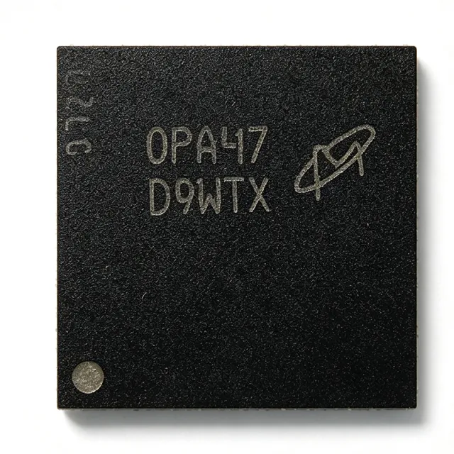
EDB1332BDBH-1DAUT-F-D - 1Gbit LPDDR2 533MHz | Micron
The Micron Technology EDB1332BDBH-1DAUT-F-D is a 1 Gbit Mobile Low-Power DDR2 (LPDDR2) SDRAM memory IC organized as 32M x 32, operating at 533 MHz with a core supply of 1.2V (1.14V to 1.95V range per Microchip USA), housed in a 134-ball VFBGA package measuring 10 x 11.5 mm for surface-mount assembly. This automotive-grade DRAM (temperature grade: automotive per Vyrian) targets space-constrained, power-sensitive embedded systems. LPDDR2 SDRAM is a memory class derived from the DDR SDRAM family, optimized for mobile and embedded applications. As part of the DRAM -> SDRAM -> mobile memory hierarchy, LPDDR2 uses a parallel interface, low core voltage, and power-saving features such as partial-array self-refresh and deep power-down modes, making it a staple power-management-conscious choice for battery-operated and thermally constrained designs alongside application processors and SoCs. Key features include the 1 Gbit density in a wide 32-bit bus organization, a 533 MHz clock rate delivering substantial bandwidth for mid-range embedded applications, and the compact 134-VFBGA (10x11.5 mm) footprint that conserves board area in stacked or densely routed PCBs. The -D suffix indicates dry-pack moisture-barrier packaging, supporting reflow soldering without unexpected moisture exposure. Architecturally, the device operates at a 1.2V core supply, consistent with the JEDEC LPDDR2 (LPDDR2-S4) standard family, with the 32M x 32 organization allowing single-chip 32-bit memory buses or chip pairing for 64-bit buses common in automotive infotainment and telematics platforms. Typical applications include automotive infotainment and cluster displays, telematics control units, embedded vision and camera systems, and industrial HMI platforms based on LPDDR2-capable SoCs such as i.MX 6 series processors. Design consideration: LPDDR2 signal integrity demands controlled-impedance routing, length-matched address/command lines, and careful VDDQ decoupling; ball-map fanout should follow the datasheet BGA breakout guidance to minimize crosstalk on the CA bus. This page synthesizes distributor pricing, stock availability, and drop-in family alternatives not consolidated in the manufacturer part-catalog page.
EDB1332BDBH-1DAUT-F-R - 1Gbit LPDDR2 SDRAM 533MHz | Micron
The Micron Technology EDB1332BDBH-1DAUT-F-R is a 1 Gbit Mobile LPDDR2 SDRAM memory IC organized as 32M x 32 with a parallel interface running at up to 533 MHz, housed in a 134-ball VFBGA package measuring 10 mm x 11.5 mm (JEDEC package code R-PBGA-B134). LPDDR2 (Low Power Double Data Rate 2) is a JEDEC-defined SDRAM family optimized for mobile and embedded systems where power efficiency and bandwidth per watt matter more than absolute peak throughput. Within the memory hierarchy, LPDDR2 sits below DDR4 in peak bandwidth but offers significantly lower standby and operating power, a wide clock range (3 MHz to 533 MHz), and CA (command/address) pin multiplexing that reduces pin count versus classic LPDDR1. As a component category, this device belongs to the DRAM -> SDRAM -> mobile LPDDR2 -> memory IC taxonomy. Key features of this part include the 1.14 V minimum (1.2 V typical) core supply per LPDDR2-S4 standards, a 32-bit wide data bus that simplifies memory subsystem design for microcontrollers and application processors, and the compact 134-VFBGA footprint suited to space-constrained boards. The -R suffix denotes tape-and-reel delivery (factory pack quantity 1000) for automated SMD/SMT assembly. Technically, the device uses a CMOS core with internally refreshed banks, self-refresh and power-down modes that are essential for battery-powered designs, and an extended industrial temperature range of -40C to +125C, making it suitable beyond consumer mobile into industrial embedded platforms. Typical applications include battery-powered industrial HMI panels, embedded Linux single-board computers, telematics and data loggers, and portable instrumentation that pair an LPDDR2-capable SoC (such as NXP i.MX 6Solo/6DualLite families) with 32-bit-wide DRAM. When designing with this device, follow the datasheet power-ramp and ZQ calibration requirements and place VREFCA/VRREF ball decoupling exactly as specified; LPDDR2 is sensitive to supply ramp order and reference voltage drift. This page synthesizes distributor pricing, drop-in alternatives, and practical design notes not found in the manufacturer datasheet.
EDB2432B4MA-1DAUT-F-D - 2Gbit LPDDR2 SDRAM 533MHz | Micron
The Micron Technology EDB2432B4MA-1DAUT-F-D is a 2Gbit Mobile LPDDR2 SDRAM memory IC organized as 64M x 32, operating at a clock frequency of 533 MHz in a 134-ball VFBGA (10 x 11.5 mm) package. This volatile DRAM is configured as a double-die package (DDP) and is rated for the extended automotive temperature range of -40C to +125C, per the -A temperature code in the Micron part numbering scheme. Mobile LPDDR2 SDRAM (Low Power Double Data Rate 2) is a member of the DRAM family of volatile memory designed for bandwidth-per-watt efficiency in battery-powered and thermally constrained systems. Within the memory hierarchy, LPDDR2 sits below LPDDR3/LPDDR4 in speed but offers lower power consumption and a simpler interface, making it a mainstay for embedded processors and applications processors that integrate an LPDDR2 memory controller. Key features of the EDB2432B4MA-1DAUT-F-D include its 2 Gbit density in a single x32 parallel data path, 533 MHz clock operation for high sustained bandwidth, automotive-grade operating temperature support, and the compact 134-VFBGA footprint that minimizes PCB area in space-limited designs. The marking code for this device is D9WVG. Architecturally, the device uses Micron's double-die package (DDP) construction, stacking two LPDDR2 dies within the single 134-ball package to reach the 2 Gbit density. The x32 organization provides a wide parallel data bus, which suits processors whose memory controllers are natively 32-bit and eliminates the need for byte-lane pairing of two x16 devices. Typical applications include automotive infotainment and instrument clusters, telematics and ADAS sensor fusion modules, industrial HMI and embedded computing systems, and portable devices requiring low-power DRAM. The extended -40C to +125C rating makes this part especially appropriate for under-hood and high-temperature automotive environments. A key design consideration is signal integrity on the high-speed LPDDR2 command/address and data buses: fly-by routing, careful length matching, and adherence to the datasheet VDDQ termination guidelines are required at 533 MHz operation. Verify controller compatibility for LPDDR2-S4 timing, including the 1.2V core supply domain. This page synthesizes distributor pricing, drop-in alternatives within Micron's LPDDR2 family, and practical design notes not found in the manufacturer datasheet.