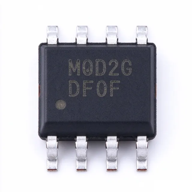
MC9S08QB8CGK
MC9S08QB8CGK - 8-bit 20MHz S08 MCU 8KB Flash | NXP
The NXP Semiconductors MC9S08QB8CGK is an 8-bit S08 microcontroller with an 8KB flash memory program area, a maximum CPU frequency of 20MHz, and a 24-HVQFN 5x5 mm package. It is designed for embedded control applications that require compact packaging, deterministic peripheral control, and low-power operation in consumer, industrial, and automotive-style embedded products.
A microcontroller is a semiconductor device that integrates a processor core, program memory, data memory, and peripherals such as timers, serial interfaces, and analog or digital I/O. The MC9S08QB8 belongs to the NXP S08 family, using the HC08 instruction set with added BGND and other S08 features. The S08 architecture is positioned between simple 4-bit controllers and more complex 32-bit processors for compact embedded control systems.
The main identifiable specifications of the MC9S08QB8CGK are its 8-bit S08 CPU, 20MHz maximum operating frequency, 8KB flash memory, and 24-HVQFN package. The available component listings also identify operation from 2.5V or 3.3V supply configurations. This combination makes the device suitable for motor control, appliance control, keypad interfaces, lighting systems, and compact industrial controllers where a small pin count and embedded flash are valuable.
The device architecture places the CPU, flash program memory, data RAM, clock, reset, and communication peripherals in one package. Its 8-bit instruction set supports embedded control workloads without requiring a separate external memory interface for firmware storage. The 20MHz clock capability provides additional timing margin for interrupt handling, periodic scanning, communications, and peripheral control, although actual firmware performance depends on the selected bus clock, peripherals, and application code.
Typical designs use the MC9S08QB8CGK as the central controller in small appliance controllers, motor or fan controls, sensor interfaces, LED lighting equipment, security panels, and low-cost industrial automation modules. The 24-HVQFN 5x5 mm package helps reduce board area, while embedded flash supports standalone firmware deployment. Designers should account for the exposed thermal-pad requirements and verify the exact pin assignment and pin functions against the NXP datasheet before layout.
The primary design consideration is ensuring that the power supply, decoupling, clock configuration, programming interface, and exposed-pad layout follow the NXP reference design. Place the required supply capacitors directly at the appropriate power pins, provide a clean ground path, and connect the exposed pad using the recommended thermal and layout pattern. Confirm programming, reset, and debug connectivity before releasing a PCB for fabrication.
This product page combines the manufacturer-associated device identity, distributor technical summaries, package details, practical application guidance, and same-family replacement analysis. It also highlights where engineers must verify detailed electrical limits, memory maps, peripheral behavior, and pin assignments directly in the NXP datasheet before final design approval.
Angebot
Kontakt