Leistungsmanagement
Unterkategorien
Produkte (2819)

INA219AIDCNR - 26V 12-bit I2C Power Monitor | Texas Instruments
The Texas Instruments INA219AIDCNR is a zero-drift, bidirectional current shunt and power monitor with an I2C- or SMBus-compatible interface, packaged in a compact 8-pin SOT-23 (DCN) package. It measures both shunt voltage drop and bus supply voltage on buses from 0 to 26 V, while operating from a single 3 V to 5.5 V supply and drawing a maximum of 1 mA of supply current. A current shunt monitor is an integrated circuit that measures the voltage across a sense resistor in series with a load, converting a small differential signal into a precise current reading. Within the power management IC hierarchy, current sense amplifiers such as the INA219 sit alongside voltage regulators and battery management ICs, providing the telemetry needed for system monitoring, protection, and efficiency optimization. The bidirectional architecture supports measurement of current flowing in both directions, essential for battery charge/discharge monitoring. Key features include a 12-bit ADC with programmable gain (0.125, 0.25, 0.5, and 1 V/V), a common-mode range of 0 to 26 V, 16 selectable I2C addresses via the A0/A1 pins, and a programmable calibration register combined with an internal multiplier enabling direct readouts of current in amperes and power in watts. The A grade provides an input offset of plus or minus 50 uV (max) and offset drift of plus or minus 0.5 uV/C (max). Technically, the zero-drift chopper-stabilized architecture maintains accuracy over the full -40C to +125C operating range. Programmable conversion time and averaging let engineers trade conversion speed against measurement noise. The SOT-23-8 package measures approximately 2.9 mm x 1.6 mm, suiting space-constrained designs. Typical applications include battery chargers, server power monitoring, telecom equipment, and power supplies, where accurate current and power telemetry is critical. It is also used in industrial load monitoring and fault detection. Design tip: place the shunt in the high-side path, decouple VS with a 0.1 uF capacitor close to the pin, and configure A0/A1 to avoid I2C address conflicts on the bus. Pricing as of 2026-08-30 from authorized distributors.
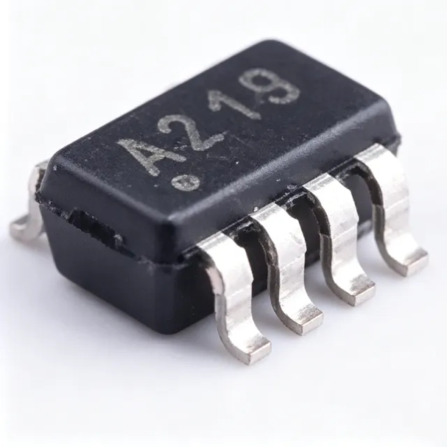
INA219AIDCNR - 26V 12-bit I2C Power Monitor | Texas Instruments
The Texas Instruments INA219AIDCNR is a zero-drift, bidirectional current shunt and power monitor with an I2C- or SMBus-compatible interface, packaged in a compact 8-pin SOT-23 (DCN) package. It measures both shunt voltage drop and bus supply voltage on buses from 0 to 26 V, operates from a single 3 V to 5.5 V supply, and draws a maximum of 1 mA of supply current. A current shunt monitor is an integrated circuit that measures the voltage across a sense resistor in series with a load, converting a small differential signal into a precise current reading. Within the power management IC hierarchy, current sense amplifiers such as the INA219 sit alongside voltage regulators and battery management ICs, providing the telemetry needed for system monitoring, protection, and efficiency optimization. The bidirectional architecture supports measurement of current flowing in both directions, which is essential for battery charge/discharge monitoring. Key features include a 12-bit ADC with programmable gain (0.125, 0.25, 0.5, and 1 V/V), a common-mode range of 0 to 26 V, 16 selectable I2C addresses via the A0/A1 pins, and a programmable calibration register combined with an internal multiplier enabling direct readouts of current in amperes and power in watts. The A grade provides an input offset of plus or minus 50 uV (max) and offset drift of plus or minus 0.5 uV/C (max). Technically, the zero-drift chopper-stabilized architecture maintains accuracy over the full -40C to +125C operating range. Programmable conversion time and averaging let engineers trade conversion speed against measurement noise, while optional filtering options improve reading stability in noisy switching environments. The SOT-23-8 package measures approximately 2.9 mm x 1.6 mm, suiting space-constrained designs. Typical applications include battery chargers, server power monitoring, telecom equipment, and power supplies, where accurate current and power telemetry is critical. It is also used in industrial load monitoring and fault detection systems. Design tip: place the shunt in the high-side path, decouple VS with a 0.1 uF capacitor close to the pin, and configure A0/A1 to avoid I2C address conflicts on the bus. This page synthesizes distributor pricing, drop-in alternatives, and practical design notes not found in the manufacturer datasheet.
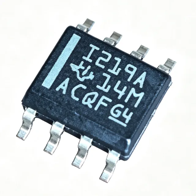
INA219AIDR - 26V 12-Bit I2C Power Monitor | Texas Instruments
The Texas Instruments INA219AIDR is a high-side, bidirectional, zero-drift current shunt and power monitor with an I2C- or SMBUS-compatible interface, packaged in an 8-pin SOIC (D). It operates from a single 3V to 5.5V supply drawing 1mA maximum, and senses across shunts on common-mode buses from 0V to 26V. The device integrates a 12-bit ADC for both shunt voltage and bus voltage, plus a 16-bit power calculation engine. A digital power monitor is an integrated circuit that measures current, voltage, and power in a system by sensing the voltage drop across a shunt resistor and the bus voltage, then converting these analog signals to digital values via an ADC and reporting them over a digital bus. It sits within the power management IC (PMIC) hierarchy, specifically under current/voltage/power monitoring ICs, which are essential for optimizing energy efficiency, protecting loads, and providing telemetry in battery-powered and industrial systems. Key features include ±1% maximum current sense error (A grade), ±50µV maximum input offset voltage, ±0.5µV/°C offset drift, 16 programmable I2C addresses, and a programmable alert pin for overcurrent or undervoltage interrupts. The shunt voltage full-scale range is ±320mV at PGA gain/1 and the bus voltage range covers 0V to 26V. The I2C interface supports standard (100kHz), fast (400kHz), and high-speed (3.4MHz) modes, with multi-device bus sharing via address pins A0/A1. Technically, the INA219AIDR uses a zero-drift chopper-stabilized front-end to minimize input offset and drift across -40°C to 125°C, eliminating the calibration burden typical of discrete current-sense amplifiers. The integrated multiplier combines shunt current and bus voltage to produce a 16-bit power reading in watts, with calibration registers that convert raw shunt voltage to engineering-unit amperes for the host MCU. Typical applications include battery monitoring in smartphones and laptops, server/telecom power supply monitoring, solar MPPT current sensing, motor current monitoring in industrial drives, and maker/hobbyist energy-meter projects using Arduino or Raspberry Pi over I2C. When designing with the INA219AIDR, place the shunt resistor in the high-side path and ensure the bus voltage stays within 0V to 26V. Decouple the supply pin with a 0.1µF ceramic capacitor close to the IC and keep I2C SDA/SCL traces short to minimize noise coupling. The ALERT pin can drive a host interrupt for immediate fault response. This page synthesizes distributor pricing, drop-in alternatives, and practical design notes not found in the manufacturer datasheet.
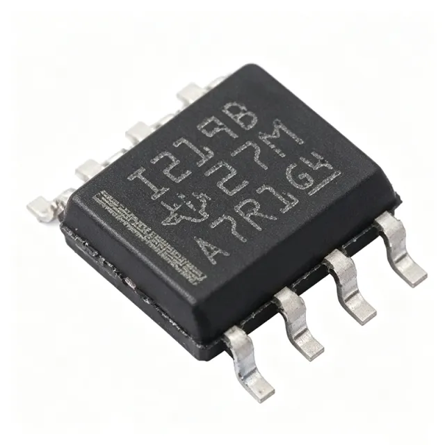
INA219BIDR - 26V 12-Bit I2C Power Monitor | Texas Instruments
The Texas Instruments INA219BIDR is a zero-drift, bidirectional current shunt and power monitor with an I2C- or SMBUS-compatible interface. It senses bus voltages from 0 to 26 V and reports current, voltage, and power through an integrated 12-bit ADC in an 8-pin SOIC package, operating from a single 3.0 V to 5.5 V supply drawing a maximum of 1 mA. The B grade offers 0.5% maximum accuracy over temperature. A current shunt monitor measures the voltage drop across a sense resistor placed in series with a load. The INA219BIDR is a digital power monitor, a subtype of current shunt monitor that integrates an ADC and digital interface to report current, voltage, and power directly to a microcontroller, fitting the hierarchy: current shunt monitor -> power monitor -> analog front-end -> signal chain IC. Key features include 16 programmable I2C addresses allowing up to 16 devices on one bus, programmable conversion times and filtering options, and a calibration register enabling direct readouts of current in amperes. An internal multiplier computes power on-chip, reducing host processor overhead. High-side sensing architecture monitors current without disturbing the ground path, critical for systems with shared grounds. The device uses a zero-drift architecture to minimize input offset voltage and drift, ensuring accuracy over temperature and time. The 12-bit ADC provides fine shunt-voltage resolution, enabling precise current sensing with minimal shunt resistance and low power loss. The I2C interface supports standard and fast modes with SMBus compatibility for server environments. Typical applications include server and telecom power management, battery chargers, embedded power supplies, test and measurement instruments, and industrial automation where accurate power telemetry is required. The 0 to 26 V bus range covers common 5 V, 12 V, and 24 V rails. Design tip: place the shunt resistor in the high-side path, keep bus voltage within 0-26 V, and use the ALERT-capable configuration to flag overcurrent events. Proper supply decoupling and short, Kelvin-connected shunt traces are essential for full 0.5% accuracy. Pricing from major distributors as of 2026-08-30.

INA223 - 26V Programmable-Gain Current Sense & Power Monitor | TI
The Texas Instruments INA223 is a voltage-output device that monitors current, bus voltage, and instantaneous power of a supply line by sensing a voltage drop across a shunt at common-mode voltages from 0 V to 26 V. It incorporates an analog multiplier to provide instantaneous power measurement, and features a two-wire and SMBus-compatible interface for adjusting configuration settings. The device operates from a single +2.7-V to +5.5-V supply, drawing a maximum supply current of 250 µA, and is specified over the extended temperature range of -40°C to +105°C. It is offered in an SON-10 package (2.5x2.5 mm). A current sense amplifier is a specialized operational amplifier designed to measure current by amplifying the small voltage drop across a shunt resistor. The INA223 belongs to the family of current shunt monitors, which are essential in power management systems for monitoring load current, supply voltage, and power consumption. These devices are critical in applications such as battery management, power supply monitoring, and system protection, where accurate current sensing is required to optimize efficiency and prevent damage. Key features of the INA223 include programmable gain via I²C, allowing the user to set the gain to 25, 50, 100, or 200 V/V, and programmable attenuation for the voltage channel. The device provides an analog output proportional to instantaneous power, which is the product of the shunt voltage and bus voltage. It also offers a high accuracy with a typical offset voltage of 50 µV and a gain error of 0.2%. The INA223 supports both high-side and low-side sensing, making it versatile for various topologies. The INA223 uses a zero-drift architecture to minimize offset drift over temperature, ensuring accurate measurements across the -40°C to +105°C range. The analog multiplier is implemented with a precision circuit that maintains linearity over the full input range. The I²C interface allows for real-time configuration changes, such as adjusting gain or enabling/disabling the device, which is useful in dynamic power management scenarios. Typical applications include server and telecom power monitoring, battery-powered devices, and industrial automation. In servers, the INA223 can monitor the power consumption of individual rails to optimize energy efficiency. In battery-powered devices, it provides accurate state-of-charge estimation by measuring current and voltage. The device's low supply current of 250 µA makes it suitable for always-on monitoring in power-sensitive applications. When designing with the INA223, ensure that the shunt resistor is placed appropriately for high-side or low-side sensing, and that the common-mode voltage does not exceed 26 V. The I²C address is set via the A0 pin, allowing up to two devices on the same bus. Proper PCB layout with Kelvin connections to the shunt is recommended to minimize parasitic resistance and maintain accuracy.

INA223AIDSKR - 26V Zero-Drift Current Sense Amplifier | TI
The Texas Instruments INA223AIDSKR is a 26 V zero-drift, programmable-gain current shunt monitor and analog power monitor with voltage output, housed in a 10-pin WSON (DSK) package measuring 2.5 mm x 2.5 mm with exposed pad. It operates from a 2.7 V to 5.5 V supply and monitors shunt voltage at common-mode voltages from 0 V to 26 V. A current sense amplifier is a specialized differential amplifier that measures the voltage drop across a shunt resistor to derive load current, and often bus voltage and power, in a power rail. It sits within the power management IC hierarchy as a current and power monitoring device, distinct from regulators or converters because it measures rather than controls energy flow. High-side and low-side placement options let designers choose between ground-path integrity and load-drop immunity. Key features of the INA223AIDSKR include bi-directional current measurement, which supports both charging and discharging current monitoring in battery systems; zero-drift architecture, which minimizes offset drift over temperature for accurate readings; programmable gain, allowing a single shunt value to cover multiple current ranges; and simultaneous current, bus voltage, and instantaneous power outputs on analog pins. The zero-drift chopper-stabilized front end delivers DC accuracy that conventional amplifiers cannot match across the automotive-industrial temperature span, while the analog output interface allows direct connection to an ADC input or comparator without serial bus programming overhead. The 0 V to 26 V common-mode range makes the device tolerant of rail transients above its own 5.5 V supply. Typical applications include battery charge and discharge monitoring in portable equipment, server and telecom power rail supervision, and power-budget telemetry in industrial automation systems where analog outputs feed system controllers or watchdog circuits. Design consideration: choose the shunt resistance to balance full-scale drop (typically 50 mV to 100 mV at maximum load) against power dissipation, and use Kelvin connections at the shunt to preserve the accuracy offered by the zero-drift input stage. This page synthesizes distributor pricing, drop-in variant cross-references, and practical design notes not found in the manufacturer datasheet.

INA226AIDGSR - 36V 16-Bit I2C Power Monitor | Texas Instruments
The Texas Instruments INA226AIDGSR is a 36 V, 16-bit, ultra-precise I2C output current, voltage, and power monitor with alert function, supplied in a 10-VSSOP (DGS) surface-mount package and specified for -40C to +125C operation. It supports both high-side and low-side shunt measurements, and bidirectional current sensing enables charge/discharge monitoring in battery and power-supply systems. A current shunt monitor is an analog-front-end IC that measures the voltage drop across a low-value external sense resistor and, together with the bus voltage, computes current and power. Within the power-management hierarchy, the INA226 sits between the power stage and the host controller: it senses the rail, digitizes data with an on-chip delta-sigma ADC, and reports over an I2C/SMBus digital bus, replacing a discrete current-sense amplifier plus separate ADC. Key features include the 36 V bus-voltage rating, 16-bit measurement resolution, programmable calibration, conversion times, and averaging, plus an integrated multiplier for direct amperes/watts readout. The I2C/SMBus-compatible interface supports up to 16 programmable addresses, and the alert pin can be programmed to respond to shunt voltage, bus voltage, or power limits, enabling fast overcurrent or undercurrent interrupts. Architecturally, the INA226 measures shunt voltage differentially across IN+ and IN- and bus voltage at the VBUS pin. The digital engine performs the multiplication, while a calibration register scales results to the actual shunt value. Programmable conversion time and averaging let designers trade speed against noise, achieving precision suited to power-rail telemetry in server, industrial, and telecom systems. Typical applications include server and datacenter power monitoring, battery charge/discharge management in portable equipment, industrial automation power rails, telecom and networking equipment, and solar inverters. The wide common-mode range and digital I2C output simplify integration with microcontrollers and BMS controllers. Design tip: place the shunt resistor close to the sense pins and use Kelvin-connected traces to minimize parasitic resistance; size I2C pull-ups correctly and configure the alert limit registers before enabling interrupts. This page synthesizes distributor pricing, drop-in alternatives, and practical design notes not found in the manufacturer datasheet.

INA228AIDGSR - 85V 20-bit I2C Power Monitor | Texas Instruments
The Texas Instruments INA228AIDGSR is an 85 V, 20-bit, ultra-precise digital power, energy and charge monitor with an I2C interface and an alert pin, housed in a 10-pin VSSOP (DGS) package. It supports bidirectional current sensing, measures shunt voltage, bus voltage, current, power, energy and charge, and is capable of being paired with an external high-voltage E3-driver for expanded transient protection. The device accepts common-mode bus voltages up to 85 V and operates over a -40 C to +125 C temperature range. An I2C power monitor is a class of analog front-end IC that digitizes the voltage across a current-sense shunt and the supply rail, then performs on-chip arithmetic to expose current, power, energy and charge over a digital bus. The INA228 belongs to the power monitor -> current sense amplifier -> power management IC -> semiconductor hierarchy, and it is commonly deployed as the housekeeping companion to a switching DC-DC converter or a battery stack, where designers need cycle-by-cycle telemetry without burdening the host MCU with analog sampling. Key features include 20-bit delta-sigma ADC core, 85 V common-mode rating, programmable gain, alert functionality for over-current or under-voltage events, on-chip temperature sensor, and 50 uA typical quiescent current. The 10-pin VSSOP (DGS) package provides a small footprint suitable for point-of-load monitoring on dense PCBs. Technically, the device combines a high-impedance front end, precision chopper-stabilized amplifiers, and a sigma-delta modulator that oversamples the differential shunt voltage. The on-chip calibration register compensates for offset and full-scale error, and the integrated temperature sensor supports system-level housekeeping. The high common-mode range allows direct connection across high-voltage battery stacks without intermediate attenuation. Typical applications include server and telecom 48 V rails, battery management systems, industrial automation, solar power optimizers, and electric vehicle DC link monitoring. The wide 85 V common-mode range makes it suitable for high-voltage battery stacks. When designing with this part, ensure the shunt resistor is sized to keep peak differential input within the device's dynamic range, and place the shunt close to the IC input pins to minimize ground-loop errors. Use the alert pin to wake the host MCU on threshold crossings instead of polling. This page synthesizes distributor pricing, drop-in alternatives and practical design notes not found in the manufacturer datasheet, giving engineers a faster path to selecting the right current-sense monitor for high-voltage rails.
INA237 - 85V 16-Bit I2C Power Monitor | Texas Instruments
The Texas Instruments INA237 is an ultra-precise digital power monitor with a 16-bit delta-sigma ADC, designed for current-sensing applications. It measures a full-scale differential input of ±163.84 mV or ±40.96 mV across a resistive shunt element, with common-mode voltage support from -0.3 V to 85 V, making it suitable for both high-side and low-side current sensing on high-voltage rails. Communication is via an I2C interface with alert functionality, housed in a 10-pin VSSOP (DGS) package. A digital power monitor is an integrated power management IC that digitizes shunt voltage, bus voltage, and computed power, then reports values over a serial bus such as I2C. Within the power-monitoring hierarchy, the INA237 sits in the current/voltage/power monitor family, complementing supervisors, hot-swap controllers, and DC-DC converters in modern power management systems. Key features include high-resolution 16-bit delta-sigma conversion, current-monitoring accuracy with ±50 uV maximum offset voltage, ±0.02 uV/C maximum offset drift, and ±0.3% gain error. The 85 V common-mode withstand is a major differentiator, allowing direct monitoring of 48 V telecom, server, and industrial buses without additional level-shifting circuitry. The delta-sigma architecture provides excellent noise performance and allows configurable conversion times and averaging, trading conversion speed for accuracy. Registers report shunt voltage, bus voltage, current, and power directly, simplifying firmware. The integrated alert pin supports configurable alerts including overcurrent and overvoltage thresholds. Typical applications include 48 V server and datacenter power-rail monitoring, telecom base-station power supplies, industrial 24-85 V motor and automation systems, and battery-management telemetry in test equipment. The wide common-mode range covers virtually all common industrial and datacenter bus voltages. Design tip: choose the shunt resistor so full-scale load current generates a shunt voltage well within the ±163.84 mV range, balancing accuracy (larger shunt) against power loss (smaller shunt). For applications needing tighter accuracy, the pin-compatible INA238 offers improved offset and gain error in the same footprint.
INA237AIDGSR - 85V 16-Bit I2C Power Monitor VSSOP-10 | TI
The Texas Instruments INA237AIDGSR is an 85 V, 16-bit, I2C-interfaced digital power monitor with alert output, housed in a 10-pin VSSOP (DGS) package. It combines a precision delta-sigma ADC, a high-accuracy internal reference, and I2C telemetry that reports current, bus voltage, power, and energy in real time across a differential shunt input of ±163.84 mV or ±40.96 mV full scale, with common-mode voltage support from −0.3 V to +85 V. The device operates from a single 2.7 V to 5.5 V supply drawing only 310 µA typical quiescent current, specified from −40 °C to +125 °C. A digital power monitor is an IC that measures current, voltage, and power by sensing the voltage drop across an external shunt resistor. It sits within the power-management IC hierarchy as a member of the current-sense amplifier family, adding a high-resolution ADC and digital interface so a host controller can read system energy usage directly. This category is essential for energy-efficient designs, load protection, predictive maintenance, and closed-loop power control in industrial, telecom, server, and automotive systems. Key specifications of the INA237AIDGSR include 16-bit ADC resolution, programmable conversion time, 16 user-selectable I2C addresses, an open-drain ALERT pin for threshold-based interrupts, ±50 µV maximum offset voltage, ±0.02 µV/°C offset drift, ±0.3 % gain error, and support for both high-side and low-side current-sensing topologies. Shunt full-scale ranges are pin-selectable between ±163.84 mV and ±40.96 mV, allowing the designer to trade dynamic range for resolution depending on shunt resistor choice. The architecture is built around a chopper-stabilized delta-sigma modulator followed by a digital filter, which converts the differential shunt voltage into a clean 16-bit code. The same device simultaneously measures the bus voltage using an internal resistor divider, eliminating the need for an external ADC channel. The I2C interface supports standard (100 kHz), fast (400 kHz), and fast-plus (1 MHz) modes, and the part integrates a robust alert/wake-up scheme that is well suited to battery-powered and always-on monitoring. Typical applications include 48 V data-center and telecom power-rail monitoring, battery management and pack telemetry, industrial 24 V bus current sensing, motor-drive and inverter DC-link monitoring, and bench test equipment. The 85 V common-mode range covers 48 V nominal rails with significant transient margin, making the INA237AIDGSR a versatile choice across high-voltage and low-voltage systems. When designing with this device, route the differential shunt traces as a Kelvin connection directly to the sense resistor pads, place a 0.1 µF decoupling capacitor close to the VDD pin, and choose 4.7 kΩ I2C pull-ups to balance rise time against bus capacitance. For AEC-Q100 requirements, select the INA237-Q1 variant. This page synthesizes distributor pricing, drop-in alternatives, and practical design notes that are not collected in any single manufacturer document.

INA3221-Q1 - 3-Ch 26V I2C Power Monitor AEC-Q100 | TI
The Texas Instruments INA3221-Q1 is an AEC-Q100 qualified, three-channel, high-side current and bus voltage monitor with an I2C- and SMBUS-compatible interface, packaged in a 16-pin VQFN (RGV) 4x4 mm package. It monitors shunt voltage drops and bus supply voltages on three independent channels with 13-bit resolution, sensing bus voltages from 0V to 26V. A current and voltage monitor (also called a power monitor or current-sense ADC) measures the voltage across a shunt resistor to compute load current, and simultaneously measures the rail (bus) voltage, reporting both digitally over a serial bus. Within the power-management hierarchy, it sits alongside current-sense amplifiers and battery-management ICs, and is fundamental to rail diagnostics in automotive, server, and industrial systems. Key features include three independent sensing channels, 13-bit conversion resolution, programmable conversion times and averaging modes, and programmable alert and warning outputs for overcurrent and undervoltage detection. The device operates from a single 2.7V to 5.5V supply, draws 350uA (typ) supply current, and offers four selectable I2C addresses for multi-device buses. Accuracy is high, with a maximum offset voltage of plus/minus 80uV and a maximum gain error of 0.25%. Technically, the INA3221-Q1 uses a zero-drift architecture that minimizes offset and offset drift over temperature, preserving accuracy across the full -40C to +125C automotive operating range. Configurable averaging trades conversion speed against noise, and the alert and critical pins allow autonomous hardware fault response without CPU intervention. Typical applications include automotive battery and multi-rail monitoring, server and telecom power-supply telemetry, and industrial automation power diagnostics. In servers it tracks CPU, memory, and peripheral rail power for energy optimization; in vehicles it supports body-control-module and infotainment rail diagnostics. Design tip: use Kelvin connections at the shunt resistors, configure I2C address pins to avoid bus conflicts, and ensure bus voltages never exceed the 26V absolute limit. Pricing references are as of 2026-08-30.

INA381A1IDSGR - 26V 350kHz Current Sense Amp w/ Comparator | TI
The Texas Instruments INA381A1IDSGR is a 26-V, 350-kHz current sense amplifier with an integrated high-speed over-current comparator, housed in an 8-pin WSON (DSG, 2x2 mm) package. It combines a wide common-mode current-shunt monitor and a comparator with an internal 1.2V reference, producing a single-chip solution for cost-sensitive overcurrent protection. The amplifier section supports both high-side and low-side current sensing and includes internal resistor gain networks that set the fixed gains for the A1/A2/A3/A4 variants. A current sense amplifier (also called a current-shunt monitor) is a type of analog signal conditioner that measures the small differential voltage developed across an external shunt resistor in the path of a load current. The output voltage is proportional to load current, enabling the system controller to monitor power, perform closed-loop current control, or trigger protection events. The INA381 sits in the hierarchy: current-sense amplifier -> analog amplifier -> signal chain IC -> semiconductor. The integrated comparator in the INA381 lets the same device assert an ALERT output when current exceeds a user-defined threshold, eliminating a separate comparator IC and shrinking the BOM in motor drive, hot-swap, and power-supply protection circuits. Key features of the INA381A1 include a 26 V common-mode range that comfortably covers 12 V and 24 V industrial buses, a 350 kHz small-signal bandwidth for fast transient response, low offset, and a propagation delay on the comparator output suitable for sub-microsecond overcurrent reaction. The amplifier supports a fixed gain (variant A1 = 20 V/V) that sets the conversion from shunt voltage to output voltage. The internal 1.2V comparator reference and open-drain ALERT output allow direct wire-OR with other system flags. The 8-pin WSON (DSG) 2x2 mm package is 24-pin, leadless, and surface-mountable, suiting dense PCB layouts. The INA381 uses a chopper-stabilized input stage and a bipolar process technology that deliver low input offset voltage and a low quiescent current. Designers can route the high-side shunt to the inputs while the comparator simultaneously watches the output against the 1.2V threshold. This eliminates timing skew between the analog measurement path and the digital protection path - a common source of nuisance tripping in discrete implementations. Typical applications include motor-drive overcurrent protection, solenoid and valve current monitoring, battery-pack current monitoring, hot-swap / eFuse circuits, USB and power-distribution load switches, and industrial 24V field-side monitoring. Compared with discrete op-amp + comparator designs, the INA381 reduces board area, BOM count, and propagation-delay variability between the measurement and the protection paths. When designing with this device, choose the shunt value so the full-scale shunt voltage is comfortably below the input common-mode and linear range, and set the comparator threshold via a resistor divider on the 1.2V reference pin. Place a 0.1 uF supply bypass capacitor close to the VDD pin to keep the chopper clock away from sensitive traces. This page synthesizes distributor pricing, drop-in alternatives, and practical design notes not found in the manufacturer datasheet.

INA4180AIPWR - 26V Quad Current-Sense Amplifier 350kHz | TI
The Texas Instruments INA4180AIPWR is a cost-optimized quad current-sense amplifier (current-shunt monitor) integrating four independent voltage-output channels in a 14-pin TSSOP (PW) package. It senses voltage drops across external shunt resistors at common-mode voltages from -0.2 V to +26 V, independent of the supply voltage, and provides rail-to-rail ground-referenced outputs proportional to load current. A current-sense amplifier is an analog IC that amplifies the small differential voltage across a sense resistor and translates it to a ground-referenced output. In the power-management hierarchy it sits between the power path and the monitoring stage, providing feedback for overcurrent protection, closed-loop current control, and load telemetry. The INA4180 integrates four such amplifiers in one IC, cutting BOM cost and board area versus single-channel INA180 or dual-channel INA2180 devices. Key features include a 350 kHz bandwidth, a common-mode range of -0.2 V to +26 V, and four rail-to-rail output channels that drive ADCs, comparators, or microcontrollers directly. Gain options of 20, 50, 100, and 200 V/V are available across the family (suffix A1-A4), set by internal matched resistor networks with low gain error and good temperature stability. AEC-Q100 qualified Q1 variants such as INA4180A2QPWRQ1 serve automotive designs. Because the common-mode range is independent of the supply, the amplifier can monitor high-side shunts on a 24 V rail while operating from a 3.3 V or 5 V supply, eliminating level-shifting circuitry. The architecture uses a precision differential front end with internal gain-setting resistors, so no external precision resistors are required. Typical applications include industrial motor control, DC-DC converter output current monitoring, battery charging systems, telecom board power monitoring, LED lighting load sensing, and automotive load detection. Design tip: use precision Kelvin connections to the shunt, place input filter resistors close to the IC, and never exceed the 26 V common-mode limit without transient protection. As of 2026-08-30, pricing data should be confirmed with distributors.

IP6537 - 20W USB PD Buck Charger SOC | Injoinic
The Injoinic IP6537 is a synchronous switch buck charger SoC with built-in power MOSFETs, designed for 20 W USB Power Delivery (PD) fast-charging adapters. It supports an input voltage range of 6 V to 32 V and provides programmable output voltages of 5 V/3 A, 9 V/2.22 A, and 12 V/1.67 A, with a maximum PD output power of 20 W. The device integrates a high-efficiency synchronous buck converter with PD protocol handling on a single die, simplifying charger and adapter designs. Key features include built-in synchronous power MOSFETs that eliminate external switches, integrated USB PD protocol support, automatic output voltage negotiation, soft-start control to limit inrush current, comprehensive protection (input OVP/UVP, output OCP/OVP/UVP, and short-circuit protection), and CV/CC output characteristics. The IC is housed in a compact 4 mm × 4 mm QFN-24 package suitable for high-density charger layouts. The IP6537 belongs to the buck converter family (step-down switching regulator -> DC-DC converter -> power management IC). A buck converter reduces a higher input voltage to a lower output voltage using a controlled switch, an inductor, and a rectifier. By integrating the high-side and low-side MOSFETs, the IP6537 shrinks the BOM versus discrete buck designs and improves efficiency, typically reaching the mid-90% range at moderate loads. Internally, the device combines a peak-current-mode buck controller with adaptive gate-drive timing and a PD protocol state machine. Built-in line-drop compensation maintains accurate output voltage under varying cable loads, while the integrated NMOS charge-pump drives the high-side switch reliably across the 6 V-32 V input range. This architecture supports constant-voltage (CV) and constant-current (CC) modes required by USB PD 3.0 PPS-style adapters. Typical applications include 20 W USB-C PD wall chargers, multi-protocol fast-charging adapters (PPS, QC), portable power banks, and 5 V-12 V auxiliary supplies in industrial equipment. The wide input range also enables 24 V bus operation in factory automation. When designing with this device, follow the inductor and capacitor selection guidelines in the manufacturer datasheet to maintain loop stability. Verify that the selected output voltage / current combinations stay within the IC's thermal envelope, especially at 12 V/1.67 A where dissipation increases with input voltage. This page synthesizes distributor pricing, drop-in alternatives, and practical design notes not found in the manufacturer datasheet.
IPD3019-760S - 19V 30W Desktop AC/DC Adapter | Inventus Power
The Inventus Power IPD3019-760S is a 30 W external desktop AC/DC adapter delivering a regulated 19 VDC output at up to 1.58 A through a 5.5 mm x 2.1 mm barrel connector. It is a Class I grounded desktop form factor, accepting a detachable IEC 60320 C14 power inlet cord (sold separately) and providing a single regulated output suitable for a wide range of 19 V nominal equipment. What is an external desktop AC/DC adapter? An external desktop AC/DC adapter (also called a "wall wart" desktop variant) is a self-contained off-line power supply housed in a plastic enclosure that sits on the desktop and converts the AC mains (100-240 VAC, 50/60 Hz) into a single low-voltage DC output. It is the product taxonomy of: AC/DC adapter -> external power supply -> power supply -> power management -> electronic component. Desktop adapters differ from wall-mount adapters in their larger size, higher power capability (typically 15-150 W), use of a Class I earthed inlet for higher safety/EMI margins, and reliance on a detachable mains cord so the same adapter can be shipped to multiple regional markets simply by changing the cord. Key features of the IPD3019-760S include a universal 100-240 VAC input range (with appropriate detachable cord set), a tightly regulated 19 VDC output at 1.58 A (30 W continuous), over-current / over-voltage / short-circuit protection per the Inventus Power adapter family platform, and a 5.5 x 2.1 mm coaxial barrel output jack. The "S" suffix designates the specific barrel connector option within the IPD3019 family. Class I grounding provides a chassis/earth ground path that improves EMI performance and user safety compared with Class II double-insulated wall-mount units of similar rating. Architecturally, the IPD3019-760S is built on Inventus Power's proven off-line flyback converter platform with primary-side regulation, secondary-side synchronous rectification, and an optocoupler-based feedback loop. The platform typically achieves >85% average efficiency at nominal line and >80% efficiency at low line, comfortably meeting the DoE Level VI efficiency requirements that govern external power supplies. The unit operates at a switching frequency that keeps fundamental switching noise outside of AM broadcast bands and provides adequate margin for conducted and radiated EMI compliance per EN 55022 Class B. Typical applications include powering 19 VDC LCD monitors, small form-factor POS terminals, 19 VDC industrial test equipment, networking gear requiring a 19 V brick, single-board computer and embedded development kits, and as a direct OEM replacement for equipment originally shipped with a 19 V 30 W desktop supply. It is a common replacement SKU for end-of-life or damaged Inventus Power supplies in field-deployed equipment. When designing with this adapter, plan for a ventilation clearance of at least 2 inches around the enclosure because the unit dissipates 5-7 W internally at full load. Verify that the load's maximum draw is below 1.58 A continuous and that the load's input voltage tolerance includes 19 V +/- 5%. Use only a detachable cord set rated for the regional mains standard. This page synthesizes distributor pricing, drop-in alternatives, and practical application notes not consolidated in any single manufacturer document.

IPS4260L - Quad 2A Low-Side Intelligent Switch | STMicroelectronics
The STMicroelectronics IPS4260L is a monolithic quad low-side intelligent power switch that integrates four independent N-channel MOSFET output stages with per-channel protection and diagnostic interfaces, each rated to 2 A continuous drain current, in a 20-pin HTSSOP package with an exposed thermal pad. The device supports switching frequencies up to 250 kHz and can drive capacitive, resistive, or inductive loads whose high-side terminal is tied to the supply rail, while its channels can be paralleled to lower on-resistance and reduce per-channel dissipation. A low-side power switch (also called a low-side driver or smart high-side switch's complement) is a power distribution building block that controls current flow between a grounded load and the return path. Compared with high-side switches, low-side drivers simplify gate drive requirements because the source sits on ground, but they cannot protect the load from supply shorts. The IPS4260L belongs to the broader category of intelligent power switches (IPS) within power management ICs, which integrate MOSFETs, gate drivers, current limiting, thermal protection, and fault feedback into a single die - a substantial integration step beyond discrete MOSFETs or relay-based switching. Key features of the IPS4260L include per-channel independent control, 2 A continuous current per channel (with paralleling supported), built-in protection against over-current, over-temperature, short circuit to VCC, and ground-loss, plus open-drain diagnostic outputs that signal fault conditions to a host microcontroller. The monolithic construction eliminates wiring parasitics and improves thermal coupling, while the HTSSOP-20 exposed-pad package provides low thermal resistance for sustained high-current operation without external heatsinking. Architecturally, each channel of the IPS4260L combines a vertical N-channel power MOSFET, a charge-pump gate driver (needed because the source rises with the load during switching), accurate current-limit circuitry, and a thermal sensor. The fault logic consolidates protection events and reports them through a shared status interface, simplifying host-side firmware and reducing MCU GPIO count on multi-channel boards. Typical applications include programmable logic controller (PLC) digital outputs, industrial solenoid and valve drivers, relay replacement in automation cabinets, multi-channel LED driving, and general low-side switching in factory automation, building control, and process control systems. When designing with the IPS4260L, observe the derating guidelines in the manufacturer datasheet: parallel channels reduce channel-to-channel temperature rise; PCB layout should maximize copper area under the exposed pad and minimize loop inductance on the switching path to limit voltage transients on inductive loads. A freewheeling (clamp) diode is generally not needed because the device includes internal avalanche-rated MOSFETs, but external protection may still be required for very high energy inductive loads.
IPS4260LM - Quad Low-Side Intelligent Power Switch | STMicroelectronics
The STMicroelectronics IPS4260LM is a monolithic quad low-side intelligent power switch capable of switching up to 2 A continuous per channel (250 kHz max PWM), housed in a 20-pin HTSSOP package with exposed thermal pad. It integrates four independent N-channel MOSFET outputs to drive resistive, capacitive, or inductive loads connected to a common supply rail, while the low-side switch topology returns load current to ground. An intelligent power switch (IPS) is a category of smart power IC that combines one or more power MOSFETs with protection, diagnostic, and interface logic in a single die. IPS parts sit hierarchically as: power switch -> load driver -> power management IC -> semiconductor. They are commonly used in industrial digital outputs, programmable logic controller (PLC) interfaces, and micro-controller expansion where reliable switching, fault feedback, and minimal external circuitry are required. Key features include four independent 2 A channels, an internal charge pump generating a gate drive, integrated over-current and over-temperature protection, per-channel open-drain status flag outputs, and compatibility with 3.3 V or 5 V logic-level inputs. The device operates from 8 V to 50 V load supply, with a typical Rds(on) of 0.3 ohm per channel at 25 C, ensuring low conduction loss in industrial 24 V systems. The IPS4260LM uses a vertical power MOSFET process with an embedded charge pump, enabling low-loss switching at high PWM frequencies up to 250 kHz. Built-in programmable current limiting, thermal shutdown with auto-retry, and per-channel diagnostics reduce MCU firmware overhead while providing robust protection against short circuits and load wiring faults. Typical applications include industrial digital output modules (24 V solenoids, relays, valves), PLC and STM32 Nucleo expansion boards, building automation, low-side lamp drivers, and motor direction/half-bridge switch legs with paired high-side companion parts. Its 50 V absolute maximum also makes it suitable for process control and HVAC actuator interfaces. When designing with the IPS4260LM, ensure the exposed thermal pad is soldered to a minimum 1 sq inch copper pour and place bypass capacitors within 5 mm of VCC and GND. Validate inrush behavior for capacitive loads because the internal current limit may trip; consider soft-start firmware if high-C loads are required.

IPS521R - 5A Fully Protected High Side MOSFET Switch | Infineon
The Infineon IPS521R is a fully protected five-terminal high-side intelligent power switch (IPS) housed in a TO-220-5 package. It integrates a vertical N-channel power MOSFET with built-in short-circuit, overtemperature, ESD protection, inductive load handling, and diagnostic feedback. The output current is internally limited to a regulated Ilim value when the load tries to exceed the safe operating area, while an active clamp absorbs the inductive kickback during load turn-off. According to the Infineon/International Rectifier datasheet, the device targets 24V industrial and automotive relay-replacement applications where a single chip must replace a discrete MOSFET plus fuse plus protection circuitry. A high-side switch (HSS) is a power-distribution topology that places the switching element between the positive supply rail and the load, returning load current to system ground. Compared with a low-side switch, a high-side switch simplifies load wiring, eliminates ground-referenced load returns, and allows direct interface with logic inputs while providing inherent protection against short-to-ground events. The IPS521R is therefore classified within the broader hierarchy: intelligent power switch -> high-side driver -> power distribution switch -> power management IC. Key features include a 5A continuous load current rating, integrated active over-temperature shutdown with auto-restart, current-limit foldback, open-load detection in the off state, status feedback through an isolated logic ground, and ESD protection on every pin. The logic ground terminal allows the device to be driven from a low-voltage microcontroller without ground-shift issues, and the diagnostic flag can be wired directly to an MCU interrupt to report fault conditions. The IPS521R is built on International Rectifier's proprietary HEXFET power-MOSFET process combined with mixed-signal CMOS control, yielding a single monolithic die that contains both the power stage and the protection logic. The active clamp structure uses the MOSFET body-drain avalanche capability to absorb unclamped inductive transients, which is critical when switching solenoids, relays, and motors that store energy in their windings. Typical applications include industrial PLC output modules, automotive body electronics (lamp drivers, solenoid drivers, valve drivers), 24V building automation, and battery-powered equipment requiring eFuse-style protection. The device is pin-compatible with the legacy IPS521 and IPS521S families, simplifying existing designs. When designing with the IPS521R, ensure adequate heatsinking for the TO-220 tab and respect the SOA envelope for inrush loads such as incandescent lamps and motor startup. Decouple Vcc with at least 1uF of low-impedance capacitance placed within 5 mm of the supply pin.

IPS521S - 5V High-Side Smart Power Switch 1.9A | Infineon
The Infineon IPS521S is a fully protected five-terminal high-side N-channel power MOSFET switch in a D2PAK (SMD-220, 5-lead) surface-mount package, delivering up to 1.9 A continuous output current and qualified for an operating supply range typically used in 5 V to 35 V load-driving systems. The device integrates short-circuit current limiting, over-temperature shutdown with auto-restart, ESD protection, active inductive clamp, open-load detection, and a diagnostic status feedback pin, forming a complete Intelligent Power Switch (IPS) block. According to the manufacturer datasheet referenced by DigiKey and Mouser listings, the output is actively limited to Ilim when an overload event occurs and the device automatically recovers once the fault is removed. A high-side switch is a power-MOSFET or intelligent-power stage placed between the positive supply rail and the load, allowing the load to be turned on and off with a low-voltage logic signal referenced to ground. Compared with a low-side switch, a high-side topology breaks the load's return-path current when off, which is the preferred configuration for safety-critical switching of lamps, solenoids, relays, and motor windings where a low-side switch would leave dangerous voltages exposed to chassis ground. The IPS521S belongs to the broader category of Intelligent Power Switches (IPS), which integrate the power FET, gate driver, protection logic, and diagnostics into a single IC to replace discrete MOSFET-plus-driver designs. Key features include logic-level CMOS-compatible input, isolated logic ground for noise-immune control, open-drain diagnostic feedback, low quiescent current in standby, and built-in active clamp for driving inductive loads such as solenoids, relays, and DC motors without external freewheeling diodes in many applications. The D2PAK package provides a low thermal resistance of approximately 50 C/W junction-to-ambient on a standard JEDEC test board, enabling continuous 1.9 A operation with adequate PCB copper area. Operating junction temperature spans -40 C to +150 C, suiting industrial and automotive underhood environments. The IPS521S uses an N-channel MOSFET on the high side driven by an internal charge pump, allowing very low Rds(on) (tens of milliohms) and therefore low conduction loss. The integrated current-limit loop folds the output characteristic back when load current exceeds Ilim, protecting the FET and wiring, while the thermal sensor forces a shutdown-and-auto-restart cycle if Tj exceeds the protection threshold. Status feedback reports fault conditions (short circuit, open load, overtemperature) to the host microcontroller. Typical applications include automotive body electronics (lamp drivers, seat heaters, mirror heaters, wiper controllers), industrial PLC discrete outputs, 24 V solenoid and valve drivers, DC motor drivers for small brushed loads, and any 5 V/12 V/24 V high-side switching where protection and diagnostics are required. When laying out the PCB, place the IPS521S on a minimum 1 square-inch copper pour to keep the junction temperature within safe limits at full 1.9 A load. This page combines distributor pricing, parametric drop-in alternatives, and practical PCB design notes that the manufacturer datasheet alone does not surface, supporting faster sourcing decisions for engineers evaluating or replacing the IPS521S.
IPS6041PBF - 40V High-Side Switch, 2.3A, TO-220AB-5 | Infineon
The Infineon IPS6041PBF is an intelligent high-side power switch rated for 40V drain-to-source voltage and approximately 2.3A continuous load current, housed in a 5-lead TO-220AB package with an exposed tab. Designed for automotive and industrial power distribution, it integrates a vertical N-channel power MOSFET with a CMOS control section on the same silicon, providing protection and diagnostics that discrete solutions cannot match in such a small footprint. The part is lead-free (PbF suffix) and qualified to automotive-grade reliability expectations. A high-side switch (HSS) is a power-MOSFET/IC combination that controls a load by placing the switching element between the supply rail and the load, rather than between the load and ground. This topology simplifies wiring harnesses, allows multiple loads to share a common ground, and provides inherent protection against short-to-ground faults. Within the broader taxonomy, the IPS6041 sits at: high-side switch -> load driver / power distribution switch -> power management IC -> semiconductor. Equivalent common names are "smart high-side switch," "intelligent power switch (IPS)," and "protected MOSFET." Key features include over-temperature shutdown with auto-restart, short-circuit protection with internal current limiting, reverse-battery protection that turns on the MOSFET to dissipate fault energy, an active clamp for inductive loads, open-load detection in both ON and OFF states, and full diagnostic feedback through a status pin. These integrated protections reduce external component count and PCB area compared to discrete MOSFET plus fuse designs. The internal current limit is set to approximately 7A (Ilim), well above the continuous rating, so the device survives brief inrush events such as lamp cold-filament or motor-start transients without nuisance tripping. Diagnostic output (pin 4) signals fault conditions to a microcontroller via a pull-up to the logic supply, enabling OBD-compliant fault reporting in automotive body-control modules. Typical applications include automotive body electronics (lighting, door locks, window lifters, seat heaters), industrial PLC outputs, 24V solenoid and valve drivers, and any 12V/24V load that benefits from diagnostic feedback and integrated protection. When designing with this device, derate continuous current to about 1A at TA = 85C in free air, or use the exposed tab with adequate PCB copper to sustain the full 2.3A rating. This page synthesizes distributor pricing, drop-in alternatives, and practical design notes not found in the manufacturer datasheet.

IR1161LTRPBF - SmartRectifier Sync Rectifier Controller | Infineon
The Infineon IR1161LTRPBF is a SmartRectifier secondary-side synchronous rectification controller IC designed to drive an N-channel power MOSFET used as a synchronous rectifier in isolated switch-mode power supplies, housed in a 5-pin PG-SOT23-5 surface-mount package. The device senses the drain-to-source voltage of the MOSFET and switches its gate on and off to bypass the body diode during the conduction period, minimizing conduction losses; remaining off during the blocking period. What is a synchronous rectifier controller? In isolated DC-DC converters and flyback/forward topologies, the secondary-side rectifier traditionally uses a Schottky or PN-junction diode, but its forward drop (0.3-0.7 V) wastes significant power at high currents. A synchronous rectifier replaces the diode with a low-Rds(on) MOSFET, and a controller IC such as the IR1161L drives that MOSFET's gate in synchronism with the secondary current flow - effectively turning the MOSFET into a near-ideal rectifier with forward drop equal to I_load x Rds(on). This controller category sits hierarchically under: synchronous rectifier controller -> rectifier controller -> secondary-side controller -> power management IC -> semiconductor. Key features include 200 V absolute maximum drain-sense voltage, adjustable turn-off threshold, very low quiescent current, internal minimum on-time to prevent false triggering at light load, and built-in protection against MOSFET body-diode conduction. The PG-SOT23-5 package occupies less than 9 mm^2 of board area and is suitable for high-density adapters and charger designs. The IR1161 uses Infineon's proprietary adaptive turn-off algorithm that compensates for variations in MOSFET Ciss and PCB parasitics, ensuring stable operation without external RC timing components in most designs. It supports DCM, CCM, and quasi-resonant primary-side topologies, making it compatible with the Infineon ICE2/ICE3 QR and DCM PWM controllers. Typical applications include USB-PD adapters (5 V/3 A to 20 V/5 A), laptop and tablet chargers, LED driver auxiliary outputs, auxiliary rails in telecom and server power supplies, and any flyback topology where replacing the Schottky rectifier with a MOSFET improves efficiency by 2-4% at full load. The IR1161 is qualified in Infineon's 15 W 5 V USB adapter reference design. When designing, place the controller close to the synchronous MOSFET to minimize the drain-sense trace inductance. Use a 100 k-ohm bleed resistor from the MOSFET gate to source to ensure the MOSFET stays off during start-up before the IR1161 bias is established. Refer to the manufacturer datasheet for the turn-off threshold resistor calculation. This page synthesizes distributor pricing, drop-in alternatives from the IR1161 family, and practical design notes not found in the manufacturer datasheet alone.

IR11682STRPBF - 200V Dual SmartRectifier SR Controller | Infineon
The Infineon IR11682STRPBF is a dual-output secondary-side synchronous rectifier (SR) controller in an 8-pin SOIC package, designed for resonant half-bridge topologies such as LLC converters. It operates from an 8.6 V to 18 V Vcc supply, drives two external N-channel MOSFET rectifiers, and switches at up to 400 kHz to maximize efficiency in high-density AC-DC and DC-DC designs. Key features include 200 V proprietary IC technology with 4 A peak turn-off drive current, 80 ns turn-off propagation delay for minimal dead-time losses, anti-bounce logic, and undervoltage-lockout (UVLO) protection. The micropower start-up and ultra-low quiescent current reduce standby losses below ENERGY STAR and 80 PLUS requirements. A 10.7 V gate-drive clamp protects standard-level MOSFETs from over-voltage gate stress. The IR11682 uses direct VDS sensing on each MOSFET to detect conduction and turn-on/turn-off thresholds independently. Its dual-output architecture replaces two Schottky rectifiers with synchronous MOSFETs, reducing conduction loss by up to 70 percent in 12 V output rails and improving thermal performance in compact adapters. Typical applications include LLC resonant converters for telecom rectifiers, server and gaming-PC silver-box SMPS, high-efficiency notebook adapters, and industrial DIN-rail power supplies. The IR11682STRPBF is well suited for any topology where Schottky or body-diode losses dominate at light load and high frequency. When designing with this part, select MOSFETs with VDS ratings above the maximum secondary voltage plus transformer ringing margin. Place the gate drive loop area minimal, and use a low-ESR ceramic bypass at VCC within 2 mm of the IC pin. This page synthesizes distributor pricing, parametric drop-in alternatives, and practical LLC layout guidance not found in the manufacturer datasheet alone.
IR1168STRPBF - 200V Dual Smart SR Controller 8-SOIC | Infineon
The Infineon IR1168STRPBF is a 200V dual smart secondary-side rectifier driver IC designed to drive two N-channel power MOSFETs used as synchronous rectifiers in resonant converter topologies, housed in an 8-pin SOIC (NB) package. It features a 200V proprietary IC technology, supports switching frequencies up to 500 kHz, and provides a 4A peak turn-off drive current with anti-bounce logic and UVLO protection. The IC can control one or more paralleled N-MOSFETs to emulate the behavior of Schottky diode rectifiers in resonant half-bridge converters. A synchronous rectifier controller (SR controller) is a type of secondary-side power supply controller that replaces traditional Schottky diodes with low-RDS(on) MOSFETs to dramatically reduce conduction losses and improve overall efficiency. SR controllers sit within the broader power management IC hierarchy (PMIC -> power supply controller -> secondary-side controller -> synchronous rectifier driver) and are essential building blocks for high-efficiency isolated DC-DC converters used in adapters, servers, telecom rectifiers, and industrial SMPS. Key differentiating features include the dual-channel architecture that drives two rectifiers from a single IC, a wide VCC operating range of 8.6V to 18V with internal UVLO, 200V drain-to-source sensing capability for direct connection to the rectifier MOSFET drains, and 4A peak gate turn-off current that eliminates the body-diode conduction period to maximize efficiency. The integrated anti-bounce logic prevents false triggering caused by PCB parasitics and MOSFET ringing. Technically, the IR1168STRPBF uses a proprietary high-voltage IC process that integrates 200V-rated sensing transistors alongside low-voltage control logic on the same die, allowing direct sensing of the drain-to-source voltage of each rectifier MOSFET without external level-shifting circuitry. The internal state machine detects when the MOSFET channel is conducting (forward current flow) and turns the gate on, then detects the body-diode conduction and turns the gate off just before the next commutation cycle, minimizing dead time and reverse recovery losses. Typical applications include resonant half-bridge LLC converters for high-efficiency adapters, telecom and server silver-box / rectifiers, industrial SMPS modules, and any isolated DC-DC topology where two low-side rectifiers are used on the secondary side. Compared to discrete Schottky rectifiers, the IR1168STRPBF-based solution typically delivers 1-3% efficiency improvement at full load, particularly in 200W-2kW power ranges. When designing with this device, careful attention must be paid to the gate drive loop layout to minimize parasitic inductance, and the drain-to-source sensing pin connections must be kept short and direct to the MOSFET to avoid false triggering from noise. The 8-pin SOIC package provides adequate thermal performance for typical rectifier applications where gate charge losses dominate rather than IC conduction losses. This page synthesizes distributor pricing, drop-in same-package alternatives, design notes and resonant converter application context not found in the manufacturer datasheet alone.

IR2010SPBF - 200V Half-Bridge Gate Driver 3A | Infineon
The Infineon IR2010SPBF is a 200 V high- and low-side gate driver IC delivering 3 A source/sink drive current, packaged in a 16-pin SOIC. It features independent high-side and low-side referenced output channels designed to drive power MOSFETs and IGBTs in half-bridge topologies, with CMOS/LSTTL-compatible logic inputs down to 3.0 V logic and matched propagation delays of 95 ns typical. A half-bridge gate driver is a specialized power-management IC that produces two synchronized gate-drive signals - one referenced to the high-side floating supply and one referenced to ground - to alternately switch the upper and lower switches of a half-bridge power stage. Gate drivers sit hierarchically below power MOSFETs/IGBTs in the power-converter signal chain, between low-power control logic (microcontroller, PWM controller) and the high-current switching devices. They provide level shifting, bootstrap drive for the high-side switch, and strong gate drive to minimize switching losses. The IR2010SPBF features high pulse-current buffer stages designed for minimum driver cross-conduction, a typical 95 ns propagation delay matched between high and low channels, and built-in shutdown logic. With 200 V maximum offset voltage and 3 A peak gate-drive capability, it supports switching frequencies well into the audio Class D and DC-DC converter application space. The floating channel operates up to 200 V and is designed for bootstrap operation. Typical applications include audio Class D amplifiers, DC-DC converters, motor drives for small brushless DC motors, and half-bridge / full-bridge power stages in industrial controls. The wide 10 V to 20 V supply range (VCC for low side, VB-VS for high side) and matched delays make it suitable for high-fidelity audio amplification and switched-mode power supplies. When designing with this part, select the bootstrap capacitor carefully (typically 0.1 uF to 1 uF ceramic) to ensure the high-side supply is refreshed each switching cycle, and respect the absolute maximum VS offset of 200 V. This page synthesizes distributor pricing, drop-in alternatives, and design notes not assembled in the manufacturer datasheet alone.