Leistungsmanagement
Unterkategorien
Produkte (2819)

ADUM7234BRZ - 4A Isolated Half-Bridge Gate Driver, 16-SOIC | ADI
The Analog Devices ADUM7234BRZ is an isolated, half-bridge gate driver that employs Analog Devices iCoupler technology to provide independent and isolated high-side and low-side outputs. Housed in a 16-pin SOIC_N (300 mil) package, it delivers up to 4 A peak output current per channel with 1000 Vrms galvanic isolation, suiting it as a drop-in MOSFET/IGBT driver for half-bridge topologies. An isolated gate driver is a power-management interface IC that delivers gate-charge to a high-voltage transistor while maintaining galvanic isolation between the low-voltage control domain and the high-voltage switching node. In the broader component taxonomy, isolated gate drivers sit inside the power-management IC family, alongside non-isolated gate drivers, motor drivers, and LED drivers. They replace older optocoupler-plus-driver pairs by integrating the isolation barrier with the driver stage, eliminating LED aging, propagation skew, and current-transfer-ratio drift. Key features of the ADUM7234BRZ include 4 A peak drive current per output, 1000 Vrms isolation (per the Analog Devices datasheet revision B), independent high-side and low-side outputs, CMOS input logic with high common-mode transient immunity (CMTI), and low propagation delay. Combining high-speed CMOS with monolithic transformer technology, the device delivers performance characteristics superior to optocoupler-based solutions by avoiding LEDs and photodiodes. Architecturally, the ADuM7234 integrates two on-chip transformers that transmit gate-edge transitions across the isolation barrier using RF-encoded pulses, then reconstruct them as CMOS gate-drive edges on the secondary side. The output stage uses complementary push-pull CMOS drivers sized to source/sink 4 A peak, allowing direct drive of small to medium MOSFETs and IGBTs without external buffers. Typical applications include isolated half-bridge and full-bridge converters, IGBT/MOSFET gate drive for motor-control inverters, industrial fieldbus isolation (RS-485, CAN, RS-232), plasma-display drivers, and high-side switch drivers. In each case, the ADuM7234BRZ replaces an optocoupler + discrete driver with a single 16-SOIC part, reducing BOM and board area. When designing with the ADUM7234BRZ, place a 0.1 µF bypass capacitor close to each supply pin (VDD1, VDD2) and provide adequate high-side bootstrap capacitance to refresh the floating supply on every switching cycle. Note that maximum junction temperature depends on PCB copper area; the SOIC_N package relies on the lead frame and copper pour for heat dissipation. This page synthesizes distributor pricing, drop-in alternatives, and practical design notes not found in the standalone ADuM7234 datasheet, helping engineers shorten design-in cycles and BOM decisions.

AL5809-100P1-7 - 100mA Constant Current LED Driver | PowerDI-123
The Diodes Incorporated AL5809-100P1-7 is a 100 mA constant-current linear LED driver housed in a compact 2-pin PowerDI-123 surface-mount package. It operates across a wide 2.5 V to 60 V input range, providing a fixed 100 mA regulated output current with ±5% accuracy and an excellent 20 ppm/°C temperature stability. The two-terminal architecture eliminates the need for any external current-setting resistor, simplifying PCB design and reducing BOM cost. A linear LED driver, also called a constant-current regulator (CCR), is a semiconductor device placed in series with an LED string to maintain a steady current despite variations in supply voltage or forward voltage. Within the broader power management hierarchy, a CCR sits below switching LED drivers and DC-DC converters; it trades efficiency for simplicity, EMI-free operation, and the smallest possible footprint. The AL5809 family extends the CCR category into high-voltage applications up to 60 V, supporting long LED chains and offline-referenced lighting. Key features of the AL5809-100P1-7 include its floating ground design, which permits both high-side and low-side LED chain driving, and a peak voltage tolerance between input and output pins suitable for offline rectified supplies. The PowerDI-123 package offers an industry-leading thermal resistance for a 2-pin device, enabling higher LED currents without excessive junction temperature rise. The driver also includes inherent LED chain protection by virtue of its linear regulation characteristic. Typical applications include 12 V and 24 V automotive interior and exterior lamps, signage and architectural LED strips, emergency lighting and indicator LEDs, and offline LED bulbs fed by rectified mains. Because the AL5809 has no PWM or enable pin, brightness control is normally achieved by varying the forward voltage or by adding an external MOSFET in series; for PWM dimming, a logic-level FET can be switched at the CCR return path. Designers should verify that (VIN − VLED_total) × ILED does not exceed the package dissipation limit.

AL8860WT-7 - 40V 1.5A Buck LED Driver | Diodes Incorporated
The Diodes Incorporated AL8860WT-7 is a 40V, 1.5A step-down (buck) LED driver with an integrated power switch, packaged in a 5-pin TSOT-25 (TSOT-25) surface-mount package. It operates from a 4.5V to 40V input range and delivers an externally adjustable constant LED current up to 1A in the TSOT-25 package (and up to 1.5A in the MSOP-8EP variant AL8860MP-13), making it well-suited for driving single or multiple series-connected LEDs from a higher-voltage source. According to the Diodes Incorporated datasheet, switching frequency is up to 1 MHz with PWM and analog dimming supported. A buck LED driver is a switch-mode DC-DC converter topology that steps down a higher DC input voltage to a lower voltage while regulating the current through an LED string. Constant-current regulation is critical for LED brightness consistency, color stability, and lifetime because LED luminous flux is highly sensitive to forward current. The AL8860 uses a hysteresis (continuous-conduction) control scheme with an integrated 40V MOSFET switch, eliminating the need for an external power transistor and simplifying BOM cost and PCB area in lighting designs. Key features include a 4.5V to 40V wide input voltage range, an internal 40V power switch, an external sense resistor for setting LED current, integrated PWM dimming input, and analog dimming support via the CTRL pin. The device operates with high efficiency (typically >90%) across the load range thanks to its low-RDS(on) internal switch and minimal quiescent current. Hysteretic control provides excellent transient response and inherently stable operation without external compensation components. Architecturally, the AL8860 combines a bandgap reference, hysteresis comparator, gate driver, and 40V N-channel MOSFET in a single die. The sense resistor between the switch source and ground sets the peak inductor current threshold, while the CTRL/ADJ pin accepts either a PWM signal for digital dimming or a DC voltage for analog dimming down to near-zero current. The high-side drive and small TSOT-25 footprint allow compact PCB layouts in space-constrained fixtures. Typical applications include MR16/GU10 LED retrofit lamps, automotive interior and exterior lighting, signage and architectural LED strips, low-voltage industrial LED fixtures, and battery-powered portable illumination. It is also suitable for general-purpose constant-current sinks in 12V/24V LED systems. When designing with the AL8860WT-7, select the inductor value to maintain continuous conduction at the minimum LED current and verify that the input capacitor handles the ripple current at 1 MHz. Place the sense resistor as close as possible to the SOURCE pin and ground to minimize parasitic inductance that could disturb the hysteresis comparator. This page synthesizes distributor pricing, parametric cross-references, and practical design notes not found in the manufacturer datasheet alone, helping engineers select the right buck LED driver and identify drop-in equivalents.
AMC0380D - ±400V AC-Input Reinforced Isolated Amplifier | TI
The Texas Instruments AMC0380D is a precision, galvanically isolated amplifier with a high-voltage AC input, high input impedance, and fixed-gain differential output. It integrates a high-voltage resistive divider, enabling direct AC voltage sensing without external resistors. The device operates with a high-side supply (VDD1) of 3.0V to 5.5V and a low-side supply (VDD2) of 3.0V to 5.5V, in a 15-pin SSOP package with 0.65mm pitch, and is fully specified over -40C to +125C. An isolated amplifier is a signal-conditioning IC that provides galvanic isolation between its input and output, protecting low-voltage circuitry from high-voltage transients and ground loops. In the analog front-end (AFE) hierarchy, it sits between raw high-voltage sensing points and system ADCs or MCUs, and is essential in motor drives, grid infrastructure, solar inverters, and power monitoring where safety isolation and accuracy are paramount. Key features include a linear input range of +/-400V with 8.3M-ohm input impedance, an integrated high-voltage resistive divider that eliminates external resistor networks, and a second-order delta-sigma (Delta-Sigma) modulator architecture for high resolution and strong noise immunity. The fixed-gain differential output simplifies interfacing with downstream ADCs and microcontrollers, while reinforced isolation provides robust protection against high-voltage transients. Technically, the input stage drives a second-order Delta-Sigma modulator whose bitstream crosses the isolation barrier, ensuring excellent linearity and low offset drift over temperature. The differential output preserves signal integrity across the barrier and rejects common-mode noise on the low side. Typical applications include AC phase-voltage sensing in three-phase motor drives, grid-tied solar inverters, and power quality monitoring, where the wide +/-400V input range removes the need for additional scaling circuitry. When designing with the AMC0380D, maintain isolation creepage and clearance on the PCB, keep the device near the sensing point, and add a low-pass filter on the differential output to suppress modulator noise.

AMIS30522 - Micro-Stepping Stepper Motor Driver, 1.5A, SPI | onsemi
The onsemi AMIS30522 is a micro-stepping stepper motor driver for bipolar stepper motors, controlled via I/O pins and a standard SPI interface from an external microcontroller. The chip integrates a current-translation table, an on-chip voltage regulator, a reset-output and watchdog reset block, and supports a maximum phase current of approximately 1.5 A peak from an 8 V to 29 V motor supply. It is housed in a 32-pin NQFP (Pb-free) package with an exposed thermal pad that drops junction-to-ambient thermal resistance to roughly 30 °C/W when a PCB ground plane is used. What is a micro-stepping stepper motor driver? A micro-stepping stepper motor driver is an integrated circuit that translates digital step commands (clock pulses plus a direction signal) into precision-regulated phase currents in a two-phase bipolar stepper motor. Unlike simple full-step or half-step drivers, micro-stepping drivers divide each full electrical step into many smaller increments (up to 1/32 micro-step in this family), producing smoother rotation, finer angular resolution, and dramatically reduced resonance and audible noise. The driver sits in the motor-control signal chain: MCU -> SPI/STEP/DIR -> stepper driver -> H-bridge -> motor windings. Key features include programmable peak current up to 1.5 A, a built-in current-translation table that automatically handles micro-step sine profiles, integrated charge-pump for the high-side N-FETs, and a configurable slew rate that lets designers trade EMI against step rate. The on-chip 5 V regulator can supply external logic, and the watchdog/reset output simplifies MCU supervisor design. Safety features include thermal shutdown, under-voltage lockout, and short-to-ground and short-to-battery detection on the motor outputs. The AMIS30522 architecture combines a serial-control block (SPI + NXT + DIR inputs) with a dual H-bridge output stage built around on-chip N-channel MOSFETs. The internal translator tracks rotor position with the NXT clock and DIR state, generating the proper sine/cosine coil currents. SPI registers allow the host MCU to set peak current, micro-step resolution, decay mode, and slew rate; status registers expose fault conditions. The device is specified for an ambient operating temperature range of -40 °C to +125 °C (automotive-grade equivalent NCV70522) and is fully compatible with the 12 V automotive voltage environment, including load-dump and jump-start transients described in the AMIS-30522 datasheet. Typical applications include headlight leveling and adaptive headlamp stepper actuators in cars, HVAC flap and valve control in industrial equipment, XY stages and Z-axis drives in 3D printers, microfluidic pumps and analyzer positioning in medical instruments, throttle-by-wire and idle-air-control actuators, and printer/scanner paper-feed and carriage motors. The wide supply range and integrated protection make it well-suited to systems that must survive harsh electrical environments. When designing with this driver, place at least one 100 nF and one 10 µF ceramic bypass capacitor directly on the motor supply pin, and connect the exposed pad to a low-impedance ground plane with multiple thermal vias. The motor supply should be decoupled from the logic 5 V rail to prevent logic-noise coupling into the analog reference. This page synthesizes distributor pricing, drop-in alternatives, and practical design notes not found in the manufacturer datasheet alone, giving engineers a single source for parametric comparison, PCB layout guidance, and replacement selection.
AMIS30522C522 - 800mA Micro-Step Stepper Motor Driver | onsemi
The onsemi AMIS30522C522 is a 32-NQFP (7x7 mm) micro-stepping bipolar stepper motor driver delivering up to 800 mA per phase, SPI configurable for embedded system integration, and qualified for industrial and automotive applications including body and chassis systems. An stepper motor driver is an integrated power and logic IC that converts step/direction commands from a host microcontroller into precisely controlled current in each winding of a two-phase bipolar stepper motor. It sits inside the motor-control subsystem hierarchy: stepper motor driver -> motor driver -> motor control -> power management -> semiconductor. The AMIS30522C522 is part of the onsemi AMIS-30522/NCV70522 family and uses I2T100 high-voltage mixed-signal technology so analog power stages and digital control logic coexist on a single die. Key features of the AMIS30522C522 include a current-translation table for microstepping, on-chip 5 V regulator to supply external microcontrollers, programmable peak current up to 800 mA per phase, programmable slow/fast decay and PWM frequencies, integrated charge pump for the high-side transistors, SPI control interface plus dedicated step (NXT) and direction (DIR) input pins, and a watchdog reset output. The chip operates across the full automotive battery range. The integrated charge pump and bootstrap diodes minimize external component count, allowing compact PCB designs. Architecturally, the AMIS30522C522 uses a dual H-bridge power MOSFET output stage to drive both phases of a bipolar stepper with synchronous rectification. The current regulation loop runs from a sense resistor and an internal DAC reference. Microstepping is achieved via a sine-cosine weighted current-translation table, while commands integrate directly through a single NXT clock pin per step. This produces smoother rotation than full- or half-step drivers at the cost of higher switching loss. Typical applications for the AMIS30522C522 are HVAC flap and valve actuators, instrument cluster gauges, headlight leveling mechanisms, throttle-by-wire positioning, general-purpose automation stepper drives, and laboratory instrumentation. The integrated voltage regulator and watchdog simplify host MCU integration. The NQFP-32 package is suitable for both hand-soldered prototypes and high-volume automotive SMT lines. Designers should ensure adequate heatsinking because the chip can dissipate several watts at 800 mA output. Add bulk reservoir capacitors at the motor supply pin (VMOT) to absorb back-EMF, and keep the analog/digital ground returns short or the impact of motor inrush will be visible on the logic supply. The AMIS-30522 product page lists automotive-grade NCV-prefixed variants for the same lifecycle - choose NCV for automotive-qualified designs. This page synthesizes distributor pricing, drop-in alternatives, and SPI configuration notes that go beyond the manufacturer datasheet - including package-level details, microstep programming references, and practical decoupling guidance.
AMIS30542 - Micro-Stepping Stepper Motor Driver | onsemi
The onsemi AMIS30542 (AMIS-30542) is a micro-stepping stepper motor driver for bipolar stepper motors, integrating dual H-bridge power MOSFETs, an SPI-configurable micro-stepping controller, and an on-chip 5 V regulator in a single 32-lead NQFP (7x7 mm) package. The device delivers up to 1500 mA RMS phase current per coil, supports 4-bit micro-stepping up to 1/32-step resolution, and operates from a wide 6 V to 30 V motor supply with logic-compatible 3.3 V / 5 V I/O. A stepper motor driver is a power-management IC that translates low-power step/direction commands from a microcontroller into the high-current, sequenced phase currents needed to rotate a bipolar stepper motor by a precise mechanical increment. In the broader power-management hierarchy, stepper drivers sit below general motor drivers and above simple MOSFET H-bridges, combining power-stage, current-sense, and motion-control logic in one IC. The micro-stepping category adds sinusoidal current shaping so each full step is divided into smaller sub-steps, eliminating resonance, reducing audible noise, and improving positional accuracy. Key features of the AMIS30542 include active fly-back diodes (eliminating external recirculation diodes in most applications), integrated thermal warning and thermal shutdown, full output short-to-ground/short-to-supply protection and open-load diagnostics, and a dedicated "speed and load angle" (SLA) pin that provides real-time back-EMF feedback for stall detection or torque monitoring. Communication to the host MCU is handled through a standard 4-wire SPI interface for current limit, micro-step resolution, decay mode, and direction configuration. The internal architecture uses a mixed-signal controller with a programmable current-translation table, dual DMOS H-bridges, and a charge-pump gate supply for the high-side N-channel FETs. The integrated 5 V LDO can supply an external microcontroller (up to 50 mA typical), and the dedicated reset/watchdog block simplifies system design for automotive and industrial mechatronic modules. Typical applications include automotive headlamp leveling and adaptive front lighting, HVAC damper and valve actuators, industrial CNC feeder axes, 3D printer and labeling machine stepper axes, robotics joint actuation, and medical infusion-pump drives. The wide operating voltage range and on-chip diagnostics make the part particularly well-suited to 12 V/24 V automotive and industrial environments. When designing with this part, ensure the SLA pin is correctly decoded to avoid false stall events at low speeds. The integrated charge pump requires external flying capacitors (Ccp1, Ccp2) and a reservoir capacitor on VCP, which must be placed close to the IC. Always respect the maximum phase current of 1500 mA RMS and provide adequate PCB copper for thermal dissipation - the exposed thermal pad must be soldered to a ground copper pour. This page synthesizes distributor pricing, verified drop-in alternatives, and practical design notes not found in the manufacturer datasheet alone.

AMIS30542C5421G - 3.2A Bipolar Stepper Motor Driver, SPI, NQFP-32
The onsemi AMIS30542C5421G is a micro-stepping stepper motor driver for bipolar stepper motors, rated up to 3.2 A coil current, in a 32-pin NQFP (7x7 mm) package, with an SPI control interface. According to the manufacturer datasheet, the part integrates two H-bridge power MOSFET outputs, an SPI-configurable current-translation table, on-chip 5 V regulator, reset output, and watchdog reset for the host microcontroller. The device operates from a nominal 12 V motor supply (range varies by load) and supports micro-stepping up to 1/32 step resolution via SPI-programmable current levels. A bipolar stepper motor driver is an H-bridge driver IC specifically designed to commutate two-winding (bipolar) stepper motors by reversing current direction in each coil pair. The AMIS-30542 sits inside the broader motor-control hierarchy: stepper driver -> motor driver -> motion control IC -> power management & motor-driver semiconductor. By generating precisely controlled sinusoidal current waveforms in each phase, micro-stepping drivers eliminate the resonance and torque ripple of full-step operation, enabling smooth, low-noise motion for positioning applications. Key features include 3.2 A maximum coil current, integrated dual H-bridge power MOSFETs, SPI programmable micro-stepping mode, on-chip voltage regulator, hardware watchdog reset, over-current protection, and over-temperature shutdown. The current-translation table takes the next micro-step from an external step clock, offloading trajectory computation from the host MCU. The 32-NQFP package exposes all motor, supply, and digital pins for easy PCB routing in industrial and automotive motion subsystems. Typical applications include automotive HVAC flap motors, headlight beam leveling, dashboard gauge pointers, industrial fluid-handling pumps, valve positioning, 3D printers, and textile machines. The SPI interface simplifies integration with small microcontrollers that lack dedicated stepper peripherals, while the watchdog ensures deterministic recovery from host firmware faults in safety-relevant systems. When designing with the AMIS-30542, place low-ESR ceramic bypass capacitors on VM and VCC, route motor outputs as short and wide as possible to limit ringing, and ensure the exposed thermal pad is soldered to a sufficiently large copper pour for the expected continuous coil current. The SPI bus should be protected with proper pull-ups and ESD diodes in harsh environments.

AMT49100 - 80V Automotive 3-Phase MOSFET Gate Driver | Allegro
The Allegro MicroSystems AMT49100 is an 80 V-rated N-channel power MOSFET driver designed to control three external MOSFETs configured in a 3-phase bridge, architected specifically for 48 V automotive applications with high-power inductive loads such as BLDC motors and electric power steering (EPS). The part integrates three half-bridge gate drivers, an SPI-configurable diagnostics block, and ASIL features in a 48-LQFP-EP (7x7 mm) package with an exposed thermal pad. The driver accepts logic-level inputs from a host MCU and produces gate-drive signals with programmable sourcing/sinking currents to switch 48 V bus-connected N-MOSFETs efficiently. A three-phase gate driver for BLDC motors sits in the motor-driver hierarchy as a sub-category of power MOSFET gate drivers, which in turn belong to power management ICs and motor-driver ICs. These ICs sit between a low-voltage logic/microcontroller domain and a high-current 48 V or 80 V power domain, providing the level shifting, dead-time insertion, and shoot-through protection that discrete H-bridge circuits cannot reliably deliver. Without an integrated gate driver, designers would need bootstrap circuits, charge pumps, and discrete level shifters to switch the high-side N-MOSFETs in a three-phase bridge. Key features of the AMT49100 include an operating voltage range up to 80 V (suitable for 48 V automotive battery systems with transient headroom), integrated charge pump for 100% duty-cycle high-side drive, programmable gate-drive current, comprehensive diagnostics via SPI (open-load, short-to-ground, short-to-battery, over-temperature, VDS monitoring), and ASIL-oriented safety features. The exposed thermal pad and 7x7 mm outline reduce PCB footprint while supporting the thermal demands of continuous high-current motor commutation. The AMT49100 uses a sophisticated SPI-programmable architecture that lets the host MCU configure dead time, gate current, fault thresholds, and diagnostic modes. Integrated VDS sensing protects the external MOSFETs from short-circuit events, while a window watchdog and BIST features support ASIL-B/System-Level functional safety. The device operates across the full automotive temperature range and includes reverse-battery and load-dump protection typical of 48 V systems. Typical applications include 48 V electric power steering (EPS) systems, 48 V mild-hybrid e-compressors, electric superchargers, and 48 V coolant/heating pumps. The 80 V rating also accommodates 24 V commercial-vehicle applications. The combination of integrated safety features and small footprint makes the AMT49100 well suited for safety-critical automotive motor control. When designing with this device, pay particular attention to the gate-drive current programming, dead-time selection, and PCB layout of the high-current motor phases. Keep the phase traces short and use a low-impedance ground return to minimize ringing on the gate-drive signals, and follow Allegro's reference layout for the bootstrap capacitors. This page synthesizes Allegro datasheet parameters, distributor pricing and stock from DigiKey/Mouser, cross-reference alternatives for drop-in replacement, and practical design notes not found in the manufacturer datasheet alone.

AMT49413 - 3-Phase BLDC Controller and MOSFET Driver | Allegro
The Allegro MicroSystems AMT49413 is a 3-phase brushless DC (BLDC) motor controller and gate driver for external N-channel MOSFET bridges, available in a 48-pin QFN-EP (7x7) package with exposed thermal pad. Key specifications include operation from 5.5 V to 50 V supply (functional guarantee down to 5.5 V), integrated commutation logic using Hall-effect sensor inputs, fixed-frequency pulse-width modulation (PWM), and gate drive capability of greater than 10 V VGS at supplies as low as 7 V. A brushless DC motor controller is an integrated circuit that handles the commutation timing and current regulation for a 3-phase brushless motor. It sits hierarchically between the gate driver and the higher-level microcontroller (MCU) within the broader motor control subsystem. The AMT49413 combines the controller, current-sense amplifier, and gate driver into a single IC, reducing external component count and PCB area compared to discrete implementations. Key features include 100% duty cycle operation for high-speed running, synchronous rectification for reduced power dissipation, and internal current sensing with an external sense resistor. The device integrates a charge pump for the high-side gate drive, eliminating the need for an external bootstrap capacitor in many topologies. Programmable features include current-limit threshold, PWM frequency, and dead time. Typical applications include automotive cooling fans, fuel and water pumps, electric power steering systems, industrial pumps and blowers, HVAC equipment, and 48 V mild-hybrid auxiliary drives. The 50 V absolute maximum rating targets 12 V and 24 V automotive buses with transient headroom. Design tip: External MOSFET selection must consider SOA at the commutation frequency chosen; switching losses scale with fSW. The exposed thermal pad must be soldered to a sufficient copper pour (recommended 1 square inch minimum) to keep junction temperature within ratings at high continuous current.
AMT49413GEVATR - 3-Phase BLDC MOSFET Controller | Allegro
The Allegro MicroSystems AMT49413GEVATR is a 3-phase brushless DC (BLDC) motor controller and gate driver for external N-channel power MOSFETs, housed in a 48-lead QFN (7x7) package with exposed thermal pad. Designed for automotive and industrial motion control, it integrates commutation logic, fixed-frequency PWM current control, and Hall-effect sensor inputs in a single IC. Operating over a wide supply range, it drives the three half-bridges of an external MOSFET bridge for high-current BLDC motors. A BLDC motor controller is a type of motor driver IC that sequentially switches the phases of a brushless DC motor using Hall-sensor feedback to determine rotor position. The controller belongs to the broader family of motor / motion controllers, which sit within the power management IC hierarchy and form the bridge between low-power logic (microcontroller, MCU) and high-current power stages (MOSFETs, IGBTs). In the system hierarchy: BLDC controller -> motor driver -> motion controller -> power management IC -> semiconductor. BLDC motors offer higher efficiency, longer life, and lower acoustic noise than brushed DC motors, making them preferred for fans, pumps, e-bikes, and EV traction auxiliaries. Key features include integrated Hall-sensor inputs, adjustable current limit, direction and run/stop control, synchronous rectification PWM for reduced switching loss, and thermal shutdown protection. The exposed thermal pad (QFN-EP) enables direct PCB heatsinking for high-current continuous operation. Fault outputs and a serial interface are provided for MCU supervision. The 48-QFN package achieves a compact footprint suitable for space-constrained motor-drive boards. The AMT49413 uses a fixed-frequency PWM architecture with built-in dead-time generation and shoot-through protection for the external N-channel FET bridge. According to the Allegro datasheet, the PWM input can be used to provide speed and torque control, and current is regulated via an external sense resistor. The 48-QFN-EP package exposes the die to the PCB copper pour, allowing sustained high-current switching without an external heatsink. Typical applications include automotive coolant pumps, HVAC fans, e-bike traction motors, industrial blowers, robotics actuators, and white-goods compressors. The wide operating voltage range and integrated protection features suit 12V/24V/48V battery-powered systems. When designing with this device, ensure the exposed pad is soldered to a sufficiently large copper pour (>=1 sq inch) to keep junction temperature within ratings at peak motor current.
AMT49413GEVATR - 50V Brushless DC Motor Driver IC | Allegro | 48-QFN
The Allegro MicroSystems AMT49413GEVATR is a three-phase brushless DC (BLDC) motor controller IC that operates from a 5.5V to 50V supply and drives N-channel external power MOSFETs in a 48-pin QFN-EP (7x7 mm) package with an exposed thermal pad. It uses a proprietary sensorless BEMF sensing scheme to commutate the motor without Hall-effect sensors, reducing BOM cost and improving reliability in dusty or high-vibration environments. The device is the commercial-grade counterpart to Allegro's AEC-Q100-qualified A4931/A49413 automotive family, delivering equivalent control performance for industrial, appliance, and white-goods applications. A Brushless DC (BLDC) motor driver is an integrated power-electronics subsystem that converts DC bus voltage into three-phase PWM waveforms timed by the rotor's electrical position, providing higher efficiency, longer life, and lower acoustic noise than brushed DC motors. BLDC motor drivers belong to the broader hierarchy: motor driver -> power management IC -> semiconductor. The AMT49413 integrates the control logic, gate drivers, current-sense amplifier, and protection blocks that previously required a discrete MCU plus FET bridge. Key specifications include a 50V absolute maximum supply rating, integrated 5V LDO for logic supply, programmable PWM frequency, soft-start, cycle-by-cycle current limiting, fault output, and thermal shutdown. The 48-QFN-EP package provides an exposed pad that lowers junction-to-ambient thermal resistance to about 28 C/W on a 4-layer 1-oz PCB, supporting continuous output currents up to several amps depending on the external MOSFET selection. The AMT49413 uses Allegro's synchronous rectified sensorless control architecture with adjustable lead angle and dynamic overcurrent thresholds. Its bootstrap-based high-side gate driver supports 100% duty-cycle operation, eliminating the audible motor-tick that plagues 6-step commutation schemes during low-speed PWM. The IC accepts a speed command from a 0-5V analog input or external PWM and outputs a tachometer (FG) signal and direction (RD) flag for closed-loop feedback. Typical applications include sensorless BLDC fans and pumps, appliance motors (washing-machine drain pumps, dishwasher circulation pumps, refrigerator compressors), HVAC blowers, and small industrial drives. The wide 5.5V-50V input range allows direct connection to 12V, 24V, and 36V battery rails without pre-regulation. When designing with the AMT49413GEVATR, pair the IC with N-channel MOSFETs whose drain-source voltage rating exceeds the maximum DC bus by at least 30% (i.e., >=75V for a 50V bus), and place the bootstrap capacitors close to the BST-CPHx pin pairs. Verify that the chosen MOSFET's total gate charge (Qg) does not push the internal regulator below the bootstrap refresh threshold at the chosen PWM frequency. This page synthesizes distributor pricing, drop-in alternatives, and practical design notes not found in the manufacturer datasheet alone, giving procurement and design engineers a single source for the AMT49413GEVATR.

AOZ1282CI - 1.2A, 36V Buck Regulator, 450kHz, SOT-23-6 | AOS
The Alpha & Omega Semiconductor AOZ1282CI is a high-efficiency, simple-to-use 1.2A synchronous-style buck (EZBuck) regulator housed in a compact SOT-23-6 package. It operates over a wide 4.5V to 36V input voltage range, delivers up to 1.2A of continuous output current, and uses a fixed 450 kHz PWM switching frequency that simplifies external L/C selection and keeps the fundamental switching ripple above the AM band. A buck regulator (also called a step-down DC-DC switching regulator) is a power management integrated circuit that converts a higher DC input voltage into a lower DC output voltage at high efficiency by rapidly switching an internal MOSFET and storing energy in an external inductor. Within the broader power management taxonomy, the AOZ1282CI sits at the regulator level: buck regulator -> DC-DC converter -> switching regulator -> power management IC -> semiconductor. The high-side internal N-MOSFET architecture and current-mode control topology place this part in the EZBuck family, designed for compact point-of-load applications. Key specifications include a 0.8V to 36V adjustable output range via an external resistor divider at the FB pin, internal soft-start, cycle-by-cycle current limit, and over-temperature protection. The fixed 450 kHz switching frequency enables a small inductor footprint, while the wide VIN range supports both 5V, 12V, and 24V industrial bus systems with sufficient headroom. Efficiency reaches up to 95% under typical load conditions. Typical applications include 12V and 24V distributed power systems, point-of-load conversion for FPGAs, MCUs and DSPs, automotive infotainment and body electronics, industrial control boards, and battery-powered portable equipment where compact size and high efficiency are required. When designing with the AOZ1282CI, place the input ceramic bypass capacitor as close as possible to the VIN and PGND pins to minimize switching noise injection, and select an inductor with low DCR to preserve efficiency at the 1.2A load. This page synthesizes distributor pricing, drop-in same-package alternatives, and practical design notes not consolidated on any single distributor or manufacturer page.
AOZ2261NQI-11 - 28V/8A Sync Buck Regulator QFN-23 | AOS
The Alpha & Omega Semiconductor AOZ2261NQI-11 is a high-efficiency, easy-to-use synchronous DC/DC buck regulator that operates from input voltages up to 28V and supplies 8A of continuous output current with an output voltage adjustable down to 0.6V plus-or-minus 1%. It integrates both high-side and low-side MOSFETs in a compact 4mm x 4mm QFN-23L (PowerTFQFN) package with exposed thermal pad, and provides a programmable on-time from 100ns to 2.6 microseconds that lets designers trade efficiency against PCB area. A buck regulator (also called a step-down switching converter) is a type of DC/DC power converter that uses an inductor, a switch, and a rectifier to convert a higher input voltage to a lower output voltage with high efficiency. Synchronous buck regulators replace the traditional diode rectifier with a low-side MOSFET to reduce conduction loss, achieving efficiencies above 90 percent in most applications. Buck regulators belong to the voltage regulator family within the broader power management IC category, sitting architecturally between the input supply and downstream digital, analog, or RF loads. Key features of the AOZ2261NQI-11 include a wide 0.6V to 23.8V adjustable output range, VCC under-voltage lockout, cycle-by-cycle current limit, output over-voltage protection, short-circuit protection, and thermal shutdown. Internal MOSFETs and a high switching frequency capability shrink the external LC filter footprint, while the exposed pad enables direct PCB heatsinking for full 8A operation. The architecture uses constant on-time (COT) control for fast transient response and predictable loop behavior without external compensation. A 4mm x 4mm QFN-23L package with low thermal resistance allows continuous 8A delivery from nominal 12V inputs at moderate ambient temperatures. Typical applications include notebook computer core and chipset rails, 12V distributed bus point-of-load converters, networking and telecom POL supplies, FPGA and SoC core rails, and high-current industrial 24V bus conversion. Designers choose this part for compact PCB area, high efficiency at moderate loads, and proven AlphaOmega EZBuck reliability. Designers should size the input capacitor to handle the ripple current of the high-side FET, choose an inductor with low DCR and adequate saturation margin above 8A, and route the feedback trace away from switching nodes. The exposed pad must be soldered to a sufficiently large copper pour for thermal dissipation; without it the junction will overheat well before reaching 8A. This page synthesizes distributor pricing from DigiKey, Mouser, and LCSC, cross-references pin-compatible drop-in alternatives, and adds practical thermal and layout guidance not present in the stock datasheet summary.

AOZ53228QI - 2.5-18V DrMOS Power Stage | Alpha & Omega
The Alpha & Omega Semiconductor AOZ53228QI is a high-efficiency synchronous buck DrMOS smart power stage rated for a 2.5 V to 18 V power-stage input, with a separate 5 V supply for its integrated gate driver and control circuitry, in a 5 mm × 5 mm QFN package. It integrates two asymmetrical power MOSFETs, a driver, PWM control, and protection functions into one compact module. A DrMOS smart power stage is an integrated power-management device that combines a high-side MOSFET, a low-side synchronous MOSFET, and gate-drive logic. It belongs to the synchronous-buck-converter hierarchy, where a controller commands the switching devices and the module supplies efficient, high-current power conversion for demanding rails. This integration reduces external switching components while placing the driver close to the power devices. The AOZ53228QI accepts PWM or SMOD# control signals, supports 3 V and 5 V logic, and accepts Tri-State PWM. Its asymmetric MOSFET arrangement supports efficient synchronous operation, while high-accuracy temperature reporting allows the host controller to monitor thermal conditions. Cycle-by-cycle current limitation is identified by the manufacturer as an OCP/NCP-series robustness feature for voltage-regulator applications. Packaged in a 5 mm × 5 mm QFN, the AOZ53228QI is intended for compact, high-current synchronous buck designs. The verified manufacturer sources describe applications encompassing data-center, telecommunications, networking, and general high-current power-delivery systems. Its integrated driver and MOSFET power stage make it suitable when board area, switching performance, and controller interoperability are priorities. Designers should route the high-current VIN, PGND, and switch-node paths with very low resistance and inductance, while decoupling the 5 V driver supply near the module. PWM and SMOD# traces should be kept away from high-dV/dt power paths, and thermal performance must be evaluated under worst-case phase current and ambient temperature rather than assumed from package size alone. This page consolidates the verified manufacturer specifications, an observed 1,000-piece price of $1.40 as of 2026-10-21, source traceability, and practical integration guidance. Unknown electrical limits, protection thresholds, pin assignments, and unreported compliance details are not inferred; they must be confirmed in the manufacturer datasheet before design release.
AOZ5517QI-03 - 60A DrMOS Smart Power Stage | AOS
The Alpha & Omega Semiconductor AOZ5517QI-03 is a high-efficiency synchronous buck power stage module integrating two asymmetrically optimized MOSFETs (high-side + low-side) and a fully integrated gate driver into a single 31-lead QFN5x5 package. Rated for 60 A output current over a 4.5 V to 25 V input range, it accepts 5 V CMOS Tri-State PWM input and supports both PWM and FCCM control for accurate switching of the internal MOSFETs. An integrated bootstrap diode simplifies PCB layout, while features like tri-state PWM, fault reporting, and adaptive dead-time control make the AOZ5517QI-03 a versatile building block for single- and multi-phase buck regulators. DrMOS is a DrMOS-compatible integrated power stage that combines the high-side MOSFET, low-side MOSFET, and gate driver in a single optimized package, reducing parasitic inductance and loop area compared with discrete implementations. By driving the two MOSFETs from a co-located driver IC, dead-time loss is minimized, switching edges are sharpened, and PCB real estate drops dramatically versus a discrete buck stage. This category belongs to the broader family of voltage regulators (DC-DC converters, smart power stages) within power management ICs. Key electrical characteristics include 60 A continuous output current capability, an integrated bootstrap diode, and adaptive dead-time control to prevent cross-conduction. The device supports Tri-State PWM logic, FCCM forced-continuous-current mode for transient response, and PWM mode for light-load efficiency. Built-in protection features include over-temperature, over-current, and fault output signaling to the controller for graceful system response. The power stage uses AOS's proprietary trench MOSFET technology with the high-side FET optimized for low gate charge and fast switching at low duty cycle, and the low-side FET optimized for ultra-low Rds(on) to minimize conduction loss. The exposed top-side thermal pad delivers a low thermal-resistance path to PCB copper, supporting sustained high-current operation in space-constrained designs. Typical applications for the AOZ5517QI-03 include high-current single-phase and multi-phase CPU/SoC core voltage regulators in notebooks and servers, graphics-card VCORE rails, point-of-load converters in telecom switches, and high-current POL modules for AI accelerators. The integrated design dramatically shrinks BOM count and simplifies PCB layout versus an equivalent discrete synchronous buck stage. When designing with this device, ensure the 5 V bias supply (VCC) is decoupled with a 1 uF X5R/X7R ceramic placed within 25 mm of the VCC pin. The exposed thermal pad must be soldered to a continuous ground plane with thermal vias; otherwise junction temperature will rise quickly at 30 A+ loads. Avoid routing the BOOT trace under the high-side MOSFET to prevent dv/dt coupling. This page synthesizes distributor pricing, drop-in pin-compatible alternatives (same QFN5x5-31L footprint), and practical layout/design notes not directly aggregated in any individual manufacturer datasheet.

AOZ7110AI#A - PFC Power Factor Correction Controller IC | Alpha & Omega Semi
The Alpha & Omega Semiconductor AOZ7110AI#A is a Power Factor Correction (PFC) controller integrated circuit housed in an 8-pin SOIC package, designed to operate in continuous conduction mode (CCM) boost PFC topologies. As a PMIC dedicated to power management, this device provides the control, gate drive, and protection functions required to build active PFC front-end stages that meet harmonic-current standards such as IEC 61000-3-2 in switch-mode power supplies, industrial motor drives, lighting ballasts, and white-goods appliances. A Power Factor Correction controller is a specialized power-management IC that shapes the input current drawn by an offline SMPS so that it stays in phase with the AC line voltage, minimizing reactive current and total harmonic distortion. Active PFC controllers sit at the front end of AC-DC converters and typically precede the main DC-DC stage; they belong to the broader PMIC family that includes voltage regulators, supervisors, and battery management ICs. The AOZ7110AI#A provides the modulator, error amplifier, and gate driver needed to force a boost converter to emulate a resistive load seen from the AC mains. Key features expected of this controller family include peak current-mode control, under-voltage lockout (UVLO) on VCC, cycle-by-cycle current limiting, soft-start to limit inrush at AC connect, and over-temperature protection. The SOIC-8 footprint allows use in space-constrained front-end designs while keeping adequate copper area for thermal dissipation through the device pins. The 8-pin footprint is a de-facto industry standard for legacy PFC controllers such as the UC3854 simplified variants, the NCP1654, and similar parts. Typical applications for the AOZ7110AI#A include 80 W to 500 W boost-PFC stages for desktop PC power supplies, server 1U/2U front ends, e-mobility chargers under 1 kW, industrial SMPS modules, and LED driver front ends. The CCM topology it targets is the most common choice for medium-power applications where efficiency above 95% and low iTHD (typically under 5%) are required by regulatory bodies. When designing with this device, designers should follow the manufacturer's evaluation board layout to keep the current-sense resistor loop short and the gate-drive return path Kelvin-connected to the boost MOSFET source. Place the VCC bypass capacitor within 5 mm of pin 8 to ensure clean UVLO behavior and reliable start-up under cold AC conditions. This page synthesizes distributor pricing, lifecycle status, and drop-in alternative information not collected in any single distributor listing, helping buyers and design engineers quickly evaluate sourcing options for the AOZ7110AI#A.
AOZ7111AI - 350kHz CRM PFC Controller | Alpha & Omega Semiconductor
The Alpha & Omega Semiconductor AOZ7111AI is a critical-conduction-mode PFC controller operating at 350 kHz in an 8-pin SOIC package. It is designed for active boost power-factor-correction front ends used with an external MOSFET, enabling AC input rectification while shaping input current toward a near-sinusoidal profile. The verified listing identifies it as an integrated-MOSFET-free PFC controller with a 9.5 V to 12 V UVLO range. A power-factor-correction controller is a power-management IC that regulates the relationship between AC input voltage and current at the supply input. In a boost PFC stage, the controller drives an external switching MOSFET and works with the inductor, capacitor, rectifier, sensing network, and feedback loop to reduce input-current distortion and improve power factor. CRM operation places the switching cycle at critical conduction, using variable-frequency control rather than relying on a fixed-frequency pulse-width modulation scheme. The AOZ7111AI’s headline verified specifications are its 350 kHz maximum operating frequency, 9.5 V to 12 V UVLO range, and SO-8 package. It has no integrated MOSFET according to the retrieved technical data, so the switching device is external to the controller. This separation allows the power stage to be selected for the required voltage, current, switching loss, and thermal conditions rather than being fixed by the controller package. The controller is intended for offline power supplies and industrial AC-DC conversion systems where PFC is required. The CRM control architecture can reduce conduction and switching losses compared with some fixed-frequency boost approaches, although inductor ripple, EMI behavior, input-current distortion, and loop stability still require application-specific validation. The manufacturer datasheet should be consulted for startup behavior, current-sense thresholds, gate-drive limits, protection features, and recommended compensation. The principal design consideration is ensuring that the external MOSFET, inductor, current-sense network, and feedback components are compatible with the AOZ7111AI’s 350 kHz operating point. Keep the power loop compact, route high-current paths carefully, and provide filtering that addresses both conducted emissions and the switching noise generated by the boost stage. Do not infer unreported electrical limits from distributor summaries. This page combines the verified distributor and manufacturer-family references with practical engineering guidance. It also records the absence of a verified drop-in substitute set, avoiding unsupported alternatives and preserving the distinction between a genuine pin-compatible replacement and a merely similar PFC controller.
AOZ73004CQI - NVIDIA OpenVReg Multiphase Buck Controller | AOS
The Alpha & Omega Semiconductor AOZ73004CQI is a high-performance, NVIDIA OpenVReg-compliant multiphase buck controller that provides one regulated output rail and supports the PWMVID dynamic voltage interface for GPU and CPU core power. Housed in a 32-pin QFN package (QFN-32, 5x5 mm) with an exposed thermal pad, it is paired with DrMOS smart power stages to deliver scalable, high-current, multi-phase rails required by modern graphics cards, notebook platforms, and desktop CPUs. The controller supports external REFIN and PWMVID input so the output voltage continuously tracks the host processor's request across a wide duty-cycle range defined by Vmin (0% duty) and Vmax (100% duty). What is a multiphase buck controller? In the hierarchy of power management ICs, a buck controller sits above the simple buck converter and below the full PMIC: it is a control IC that drives external power-stage blocks (DrMOS / smart power stages) in parallel to deliver high currents with low ripple. By interleaving the phases (each phase shifted by 360/N degrees), the input and output ripple currents partially cancel, enabling smaller output filter inductors and faster transient response. A PWMVID controller adds a further layer: the output voltage is set point is digitally encoded as a PWM duty cycle, allowing the host (e.g., an NVIDIA GPU) to command DVFS transitions in nanoseconds without I2C or analog VID DAC overhead. Key features of the AOZ73004CQI include NVIDIA OpenVReg specification compliance, PWMVID interface with external reference input, multi-phase operation (configurable phase count), adaptive voltage positioning for transient load steps, and per-phase current sensing and balancing. The architecture supports N+1 phase redundancy, droop-free operation during dynamic VID transitions, and telemetry outputs (e.g., IMON, TMON, PGOOD) for system-level monitoring. Typical applications include GPU core power on add-in graphics cards (PCIe x16 form factor), notebook discrete GPU platforms, AI accelerator cards, and desktop CPU VCORE rails. It is also suited to any high-current digital load requiring OpenVReg-compatible DVFS control with low ripple and fast transient response. When designing the multiphase rail, careful DrMOS selection and inductor sizing are required. The output filter inductance scales inversely with the number of active phases, and the loop compensation network must be tuned to the chosen DrMOS and output capacitance. PWMVID reference integrity is critical - keep the REFIN trace short and shield it from switching noise.
AOZ73016QI - 16-Phase PMBus Buck Controller | AOS
The Alpha & Omega Semiconductor AOZ73016QI is a hybrid multiphase buck controller with dual-output support for up to 16 total phases, NVIDIA OpenVReg compliance, and a PMBus digital interface, supplied in a QFN package. The controller is designed for high-current, programmable voltage rails requiring precise telemetry, fault handling, and flexible phase allocation. A multiphase buck controller coordinates multiple high-frequency power stages to produce a single high-current output rail. By distributing current across several inductors and DrMOS or Smart Power Stage devices, this architecture reduces ripple, improves transient response, and shares thermal load. The AOZ73016QI belongs to the power-management IC hierarchy and supports configurable single-rail or dual-rail operation. The AOZ73016QI supports VR1 configurations from 0 to 16 phases and VR2 configurations from 0 to 8 phases, with total phases constrained by N+M ≤ 16. Its PMBus interface enables register programming through the AOS GUI or customized embedded controller software. The device also provides nonvolatile memory for retaining register settings. AOS Advanced Transient Modulator, or A2TM, combines variable-frequency hysteretic peak-current control behavior with programmable compensation to address load transients. The controller provides programmable protection and warning functions including UVP, OVP, OCP, and OTP. PMBus telemetry reports input voltage, output voltage, temperature, and current. Typical uses include NVIDIA OpenVReg16-compatible AI server rails, graphics-card power systems, high-current processor supplies, and other configurable multiphase power architectures. It can pair with industry-standard DrMOS and Smart Power Stage devices, allowing the power-stage selection to match current, efficiency, and thermal requirements. Designs must allocate phases correctly, connect external power stages and inductors, and validate PMBus configuration, fault thresholds, telemetry, and startup behavior. Because the supplied data does not provide complete electrical ratings, pin mapping, package dimensions, or thermal limits, engineers should use the official AOZ73016QI datasheet and product brief before layout or production release.
AOZ98252QI - 8-Phase Dual-Rail Buck Controller | AOS
Alpha & Omega Semiconductor AOZ98252QI is a high-performance digital multiphase buck controller with two programmable output rails, an aggregate M+N=8-phase configuration, and AMD SVI3 support. It is designed for processors, ASICs, SoCs, FPGAs, graphics systems, and desktop computing platforms. The verified product information identifies a low-quiescent-current architecture, digital interface control, Pulse Skipping light-load behavior, and Dynamic Phase Management (DPM). The controller uses AOS Advanced Transient Modulator (A2TM) technology, combining variable-frequency hysteretic peak-current-mode control with proprietary phase-current sensing for fast transient response and reduced system cost. The control architecture enters discontinuous conduction mode during light-load operation to improve efficiency. The controller supports AMD SVI3 2.0, high-speed digital control, and SMBus digital interfaces. It can configure VR1 for up to 8 phases and VR2 from 0 to 4 phases, allowing one device to coordinate a dual-rail processor power system. The AOZ98252QI is intended to work with external power-stage devices, such as AOS DrMOS products, rather than directly delivering the full processor output current. Use the manufacturer product page and product brief for electrical ratings, package details, pin assignments, interface timing, and application-specific design limits because those values were not supplied in the verified dataset. The device belongs to the power-management controller hierarchy: multiphase controller, buck controller, voltage regulator controller, and power-management IC. Its primary design value is coordinating multiple high-current switching phases while supporting programmable telemetry and power-state control.
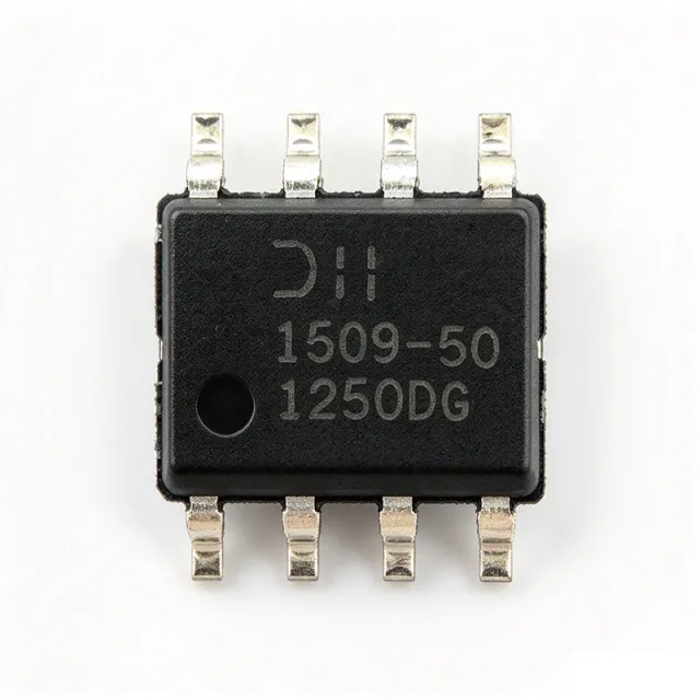
AP1509-50SG-13 - 2A, 150kHz, Fixed 5V Buck Converter | Diodes Inc.
The Diodes Incorporated AP1509-50SG-13 is a monolithic 150 kHz PWM step-down (buck) DC-DC converter in an 8-pin SOIC (SG) package with a fixed 5.0 V output and a 2 A continuous load capability from a 4.5 V to 22 V input rail. Designed as a one-chip switching regulator, it integrates the power switch, oscillator, feedback loop and protection blocks, eliminating the need for an external MOSFET and shrinking the total solution footprint for distributed 5 V point-of-load designs. A buck (step-down) DC-DC converter is a switching voltage regulator that uses an inductor-capacitor energy transfer network to convert a higher DC input into a lower, regulated DC output. Buck regulators deliver far higher efficiency (typically 80-95%) than linear regulators when the input-to-output voltage drop is large, which makes them the preferred topology for stepping down 12 V or 15 V bus rails to logic-level supplies such as 5 V, 3.3 V or 1.8 V. The AP1509-50SG-13 sits in the broader hierarchy of switching regulator -> DC-DC converter -> voltage regulator -> power management IC. Key specifications include a fixed 5 V output, 150 kHz nominal switching frequency, 2 A continuous output current, 4.5 V to 22 V input voltage range, internal MOSFET switch, and built-in thermal shutdown. The 150 kHz switching frequency allows the use of small, low-cost inductors and filter capacitors, while the SOIC-8 footprint offers the same land pattern as the popular LM2596-style 5-pin regulators with a few unused pins. This pin/effort savings is one of the device's primary value propositions. Typical applications include 12 V-to-5 V distributed power buses in consumer electronics, point-of-load regulation after a front-end AC-DC or 24 V industrial supply, battery charger auxiliaries, hobby robotics and Arduino-style 5 V rails, and any cost-sensitive board that previously used an LM7805 linear regulator and now needs higher efficiency. Designers moving from a 7805 typically see efficiency jump from ~40% to ~85% while reducing or eliminating heatsinking. When designing with this part, observe the minimum 4.5 V input headroom and choose an inductor sized for the 2 A saturation rating with low DCR for best efficiency. The AP1509 uses voltage-mode control; for noise-sensitive analog loads a small LC output filter or post-LDO can be added because the ripple at 150 kHz is typically 30-50 mV pk-pk.

AP1661AP-G1 BCM PFC Controller | Diodes Incorporated
The Diodes Incorporated AP1661AP-G1 is a boundary-conduction-mode power-factor-correction controller packaged as an 8-pin PDIP. The device is designed for high-performance PFC power conversion and uses BCM operation to support power-factor correction in switch-mode power supplies. The verified distributor data identifies a 14.5 V supply value, 50 uA startup current, and an operating temperature range of -40°C to 85°C. The AP1661AP-G1 is listed as obsolete in comparison data, so lifecycle planning should confirm availability before committing to new production. A power-factor-correction controller is a power-management semiconductor used in AC-to-DC converters and switch-mode power supplies. Its role is to shape input current so that it is drawn in phase with the AC input voltage, improving true power factor and reducing reactive current. In the broader hierarchy, this part belongs to the PFC-controller class within power-management ICs, alongside voltage regulators, DC-DC converters, supervisors, and motor-driver products. Boundary-conduction-mode control reduces conduction losses by allowing the switching device to conduct near the voltage peak and limiting high-frequency switching activity. The AP1661AP-G1 includes the key verified attributes of BCM PFC operation, an 8-pin PDIP package, through-hole mounting, a 14.5 V supply value, and a 50 uA startup current. Its operating-temperature range is specified as -40°C to 85°C. These values make it relevant to designers evaluating compact, offline power-conversion equipment, especially where a through-hole controller package and established BCM control method are preferred. The package is listed as 8-DIP with a 0.300-inch, 7.62 mm lead pitch in the comparison data. AP1661AP-G1 is commonly associated with PFC stages in offline power supplies, industrial AC-DC converters, appliance power systems, and other mains-powered equipment. The controller coordinates the switching behavior of an external power stage rather than directly regulating an output voltage alone. External magnetics, switching devices, sensing networks, and safety circuitry remain necessary to complete a practical PFC design. Component selection should therefore include validation of switching frequency, current sensing, protection thresholds, startup behavior, and thermal conditions from the manufacturer datasheet. For hardware design, use the manufacturer datasheet and application guidance to select the gate-drive network, current-sense resistor, compensation components, input bridge, output capacitor, boost inductor, and EMI filtering. Keep the high-current switching loop compact and keep sensitive feedback and current-sense traces away from power-node transitions. Because the verified data marks the part obsolete, new designs should confirm lifecycle status, stock, and approved sourcing before layout release. This product page consolidates the verified distributor identity, BCM PFC classification, package information, lifecycle observations, and engineering application guidance for AP1661AP-G1. It distinguishes confirmed values from unavailable specifications and avoids treating similar AP1661 variants as drop-in replacements without explicit evidence.
AP1661MTR-E1 - 0.8A PFC Controller | Diodes Incorporated
The Diodes Incorporated AP1661MTR-E1 is a boundary-conduction-mode power-factor-correction controller with a listed 14.5 V input and 0.8 A output rating, packaged in an 8-pin SOIC. It is designed primarily as the active controller for a boost pre-converter in AC power supplies, where it helps shape input current and reduce reactive power. The verified data identifies the device as an active PFC controller, with an operating temperature range of -40 °C to +85 °C. A power-factor-correction controller is a power-management semiconductor that controls the charging of an energy-storage inductor in an AC-input boost stage. By commanding the switching device according to a suitable conduction method, the controller helps the upstream rectifier draw current near the input-voltage waveform instead of narrow, highly reactive pulses. The result is improved input power factor and lower line-current distortion when paired with the correct power stage and compensation network. The AP1661MTR-E1 uses boundary-conduction mode, identified in the distributor data as BCM. This mode is associated with a boost PFC stage and can simplify control compared with continuous-conduction implementations when the surrounding inductor, switching element, sensing network, and compensation are designed for the intended line input. The verified listing also specifies an SOIC-8 package and a RoHS-compliant part. The listed 0.8 A output and 14.5 V input values should be treated as the available verified parameters, not as a complete electrical rating set. The manufacturer datasheet is required for pin names, thresholds, gate-drive limits, compensation details, start-up behavior, and absolute maximum ratings. AP1661MTR-E1 is marketed as an active component in the retrieved data, while procurement availability and pricing vary by distributor. Typical applications include front-end PFC for industrial power supplies, server and telecom power systems, and AC-DC converters that require reduced input-current distortion. In each case, the controller is only one part of the solution; the boost inductor, switching transistor, rectifier bridge, capacitors, current-sense network, and feedback loop determine the achieved power factor and efficiency. A critical design consideration is validating the complete PFC loop against the minimum and maximum input line, output voltage, load, and switching frequency. Do not infer pin functions, protection behavior, or maximum output power from the distributor summaries alone. Use the manufacturer datasheet and validate startup, overvoltage, overcurrent, zero-cross behavior, and thermal conditions in the target enclosure.