K3LK8K80CM-MFCP vs K3LKBKB0BM-MGCP Vergleich
Detaillierter Direktvergleich von K3LK8K80CM-MFCP von Samsung Electronics und K3LKBKB0BM-MGCP von Samsung Electronics. Vergleichen Sie die wichtigsten Spezifikationen, elektrischen Parameter, Gehäuse, Lebenszyklusstatus, Preise und Verfügbarkeit, um das beste Bauteil für Ihre Designanforderungen zu ermitteln.

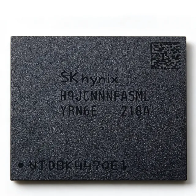
Spezifikationsvergleich
| Parameter | K3LK8K80CM-MFCP | K3LKBKB0BM-MGCP |
|---|---|---|
| Marke | Samsung Electronics | Samsung Electronics |
| Kategorie | Memory ICs | Memory ICs |
| Lebenszyklusstatus | Aktiv | Aktiv |
| Lagerstatus | In Stock | In Stock |
| Stückpreis (USD) | $0,00 | $46,62 |
| Speichertyp | LPDDR5 SDRAM | DRAM (LPDDR5 SDRAM) |
| Density | 48 Gbit (6 GB) | — |
| Speicherorganisation | [DATA_NEEDED: organization (x width)] | 1G x 32 |
| Pin Speed | 6400 Mbps | — |
| Data Rate (package) | 51.2 GB/s (family max) | — |
| Schnittstelle | LPDDR5 (JESD209-5 class low-power DRAM interface) | LPDDR5 x32 |
| Gehäuse | 315-ball FBGA (MFCP) | FBGA-315 |
| Ball Count | 315 | — |
| Montageart | Surface Mount | Surface Mount |
| Betriebstemperatur | -40 C to +105 C (automotive-grade) | -25C to +85C |
| Versorgungsspannung | [DATA_NEEDED: VDD/VDDQ voltage] | — |
| Power Saving vs LPDDR4X | Approximately 20% | — |
| Generation | LPDDR5 (5th generation low-power DRAM) | — |
| Application Grade | Automotive-grade storage chip | — |
| Place of Origin | Johor, Malaysia | — |
| RoHS-Status | unknown | Compliant |
| Speichergröße | — | 32 Gbit |
| Datenrate | — | 6400 Mbps per pin |
| Supply Voltage Rails | — | 500 mV, 900 mV, 1.05 V, 1.8 V |
| Technology Generation | — | LPDDR5 (JEDEC LPDDR5 family) |
| Density per Package | — | 4 GB (32 Gbit) |
| Refresh | — | Self-refresh and auto-refresh (LPDDR5 standard) |
| Application Segment | — | Mobile, embedded, industrial computing |
| Standby / Deep Sleep | — | LPDDR5 deep-sleep power states |
| MSL-Level | — | [DATA_NEEDED: MSL level] |
| Access Time / Latency | — | [DATA_NEEDED: CAS latency] |