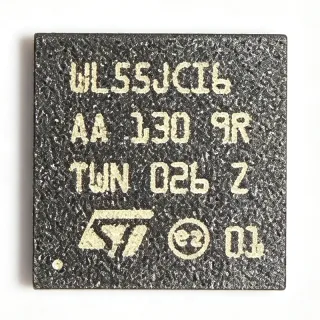
AD9082BBCZ - Quad 12GSPS RF DAC & Dual 6GSPS ADC | Analog Devices
Teilenummer: AD9082BBCZ ✓ Aktiv| Menge | Stückpreis | Gesamt |
|---|---|---|
| 1 | $1488.91 | $1.488,91 |
| 10 | $1400 | $14.000,00 |
| 100 | $1300 | $130.000,00 |
| 500 | $1200 | $600.000,00 |
| 1.000 | $1100 | $1.100.000,00 |
AD9082BBCZ Übersicht
A mixed-signal front-end (MxFE) is a single-chip solution that integrates high-speed data converters with digital signal processing blocks, enabling direct RF sampling and synthesis. It sits between the analog RF domain and the digital baseband processor, replacing multiple discrete components. The MxFE hierarchy includes RF transceiver -> mixed-signal front-end -> data converter -> semiconductor, streamlining system design and reducing board space.
Key features of the AD9082 include a flexible reconfigurable common platform design, supporting 4 DACs and 2 ADCs (4D2A) and 2D2A options. It supports single, dual, and quad band operation, with fully bypassable datapaths and DSP blocks. The device offers DAC to ADC sample rate ratios of 1, 2, 3, and 4, and includes an on-chip PLL with multichip synchronization. These features enable direct RF sampling at frequencies up to 6 GHz for the ADC and 12 GSPS for the DAC, eliminating the need for multiple up/down conversion stages.
Technically, the AD9082 integrates a 16-bit DAC core operating at up to 12 GSPS, providing high dynamic range and low noise for transmit paths. The 12-bit ADC core samples at up to 6 GSPS, capturing wideband signals directly at RF frequencies. The on-chip DSP blocks allow for digital up/down conversion, filtering, and gain adjustment, reducing the processing load on the FPGA or ASIC. The device supports JESD204B/C serial interfaces for high-speed data transfer to and from digital processors.
Typical applications include 5G NR base stations, phased array radar, electronic warfare, and wideband software-defined radios. The AD9082's ability to handle multiple bands and channels simultaneously makes it suitable for massive MIMO systems and spectrum monitoring. Its high sample rates and direct RF sampling capability reduce system complexity and power consumption compared to traditional heterodyne architectures.
When designing with the AD9082, careful attention must be paid to power supply decoupling and thermal management. The device requires multiple supply rails, and proper layout of the high-speed digital and analog interfaces is critical to achieve specified performance. The on-chip PLL requires a clean reference clock, and the JESD204B/C interface must be configured correctly for reliable data transfer.
Drop-in-Alternativen für AD9082BBCZ – gleiches Gehäuse, Pin-kompatibel. Bauteile mit anderem Gehäuse, die eine PCB-Überarbeitung erfordern, sind ausgeschlossen.
Varianten dieser Serie
Modelle derselben Serie, die drop-in-kompatibel sind mit AD9082BBCZ (gleiche Bauform und Footprint) – abweichend in Package, Number of DACs, ADC Maximum Sample Rate, Core Supply Voltage, Data Interface.
Schnellvergleichstool – Wählen Sie Alternativbauteile für den Direktvergleich:
AD9082BBPZ-2D2AC
✅ Drop-In📋 Referenzalternative (nicht im Katalog)
AD9081BBCZ
✅ Drop-In ⚠️ Spezifikationen ungeprüft✓ Auf Lager
$1082.84 / Stück
Datenblatt ansehen →AD9174BBCZ
✅ Drop-In ⚠️ Spezifikationen ungeprüft✓ Auf Lager
Preis auf Anfrage
Datenblatt ansehen →AD9173BBCZ
✅ Drop-In ⚠️ Spezifikationen ungeprüft✓ Auf Lager
$120 / Stück
Datenblatt ansehen →AD9172BBCZ
✅ Drop-In ⚠️ Spezifikationen ungeprüft✓ Auf Lager
$59.7 / Stück
Datenblatt ansehen →AD9082BBCZ Grenzwerte & elektrische Eigenschaften
| DAC Resolution | 16-bit |
| DAC Maximum Sample Rate | 12 GSPS |
| ADC Resolution | 12-bit |
| ADC Maximum Sample Rate | 6 GSPS |
| Number of DACs | 4 |
| Number of ADCs | 2 |
| Gehäuse | 324-BGA-ED (15x15 mm) |
| Montageart | Surface Mount |
| Betriebstemperaturbereich | -40°C to +85°C |
| Schnittstelle | JESD204B/C |
| On-Chip PLL | Yes |
| Multichip Synchronization | Yes |
| RoHS-Status | Compliant |
AD9082BBCZ Pin-Konfiguration
| Pin A1 | VDD — Power supply |
| Pin A2 | GND — Ground |
| Pin B1 | DAC0_P — DAC output positive |
| Pin B2 | DAC0_N — DAC output negative |
| Pin C1 | ADC0_P — ADC input positive |
| Pin C2 | ADC0_N — ADC input negative |
| Pin D1 | CLK_P — Clock input positive |
| Pin D2 | CLK_N — Clock input negative |
| Pin E1 | SYSREF_P — System reference positive |
| Pin E2 | SYSREF_N — System reference negative |
| Pin F1 | SPI_CS — SPI chip select |
| Pin F2 | SPI_CLK — SPI clock |
Typische Anwendungen
AD9082BBCZ ist geeignet für 6 Anwendungs: 5G NR Base Stations, Phased Array Radar, Electronic Warfare, Software-Defined Radio, Test and Measurement, Satellite Communications.
5G NR Base Stations
The AD9082BBCZ is ideal for 5G NR base stations, providing direct RF sampling for multiple bands and channels. Its quad 12 GSPS DAC and dual 6 GSPS ADC support massive MIMO and carrier aggregation, reducing system complexity and power consumption. The on-chip PLL and JESD204B/C interface simplify integration with baseband processors, enabling high data throughput and low latency.
Empfohlen
Phased Array Radar
In phased array radar systems, the AD9082BBCZ enables direct RF sampling of multiple channels, improving target detection and beamforming accuracy. Its high sample rates and multichip synchronization support coherent processing across many elements. The device's flexible datapath and DSP blocks allow real-time calibration and adaptive beamforming, enhancing radar performance in dynamic environments.
Empfohlen
Electronic Warfare
The AD9082BBCZ is well-suited for electronic warfare systems that require wideband signal detection and jamming. Its dual 6 GSPS ADC captures a broad spectrum, while the quad 12 GSPS DAC generates agile jamming signals. The device's fast reconfiguration and bypassable DSP blocks enable rapid response to changing threats, making it a critical component in modern defense electronics.
Empfohlen
Software-Defined Radio
In software-defined radios, the AD9082BBCZ provides a flexible RF front-end that can be reconfigured for different frequency bands and waveforms. Its direct RF sampling eliminates multiple conversion stages, reducing size, weight, and power. The device's JESD204B/C interface connects seamlessly to FPGAs, enabling software-defined modulation and demodulation for military and commercial communications.
Empfohlen
Test and Measurement
The AD9082BBCZ is used in high-end test equipment such as arbitrary waveform generators and spectrum analyzers. Its 12 GSPS DAC generates wideband signals with high fidelity, while the 6 GSPS ADC captures fast transients. The device's on-chip DSP enables real-time signal processing, making it ideal for automated test systems that require precise, repeatable measurements.
Empfohlen
Satellite Communications
For satellite communication ground stations, the AD9082BBCZ supports wideband multi-carrier operation, enabling high-throughput links. Its direct RF sampling reduces the need for multiple downconverters, simplifying the RF chain. The device's multichip synchronization ensures coherent processing across multiple channels, which is essential for phased array antennas and beamforming in satellite systems.
Empfohlen
Zusammenfassung der empfohlenen Produkte
Technische Referenzdaten für AD9082BBCZ – Vergleich, Designhinweise und Compliance-Informationen.
Auswahlhilfe
Vergleich mit Alternativen
| Parameter | Dieses Produkt | AD9082BBPZ-2D2AC | AD9081BBCZ | AD9174BBCZ |
|---|---|---|---|---|
| Package | 324-BGA-ED (15x15) | 324-BGA-ED (15x15) | 324-BGA-ED (15x15) | 324-BGA-ED (15x15) |
| Brand | Analog Devices | Analog Devices | Analog Devices | Analog Devices |
| DAC Resolution | 16-bit | 16-bit | 16-bit | 16-bit |
| DAC Sample Rate | 12 GSPS | 12 GSPS | 12 GSPS | 12.6 GSPS |
| ADC Resolution | 12-bit | 12-bit | 12-bit | N/A (DAC only) |
| ADC Sample Rate | 6 GSPS | 6 GSPS | 6 GSPS | N/A (DAC only) |
| Number of DACs | 4 | 4 | 4 | 4 |
| Number of ADCs | 2 | 2 | 4 | 0 |
Wichtigste Unterscheidungsmerkmale
- Integrated quad DAC and dual ADC in one package (vs. AD9174BBCZ)
- Higher ADC channel count (vs. AD9082BBPZ-2D2AC)
- Direct RF sampling capability (vs. AD9174BBCZ)
Designhinweise
The AD9082BBCZ requires multiple power supply rails with low noise and good decoupling. Use ferrite beads and 10uF + 0.1uF capacitors on each supply pin. Ensure the analog and digital supplies are properly separated to avoid noise coupling. Refer to the datasheet for recommended supply sequencing.
The AD9082BBCZ dissipates significant power, especially at high sample rates. Use a thermal pad and adequate PCB copper area for heat sinking. The 324-BGA-ED package has an exposed pad that must be soldered to a thermal via array. Monitor junction temperature to stay within the -40°C to +85°C operating range.
For high-speed JESD204B/C interfaces, maintain controlled impedance traces (typically 100 ohm differential) and keep trace lengths matched. Place the device close to the FPGA to minimize skew. Use ground planes under the device and avoid routing high-speed signals over split planes.
Compliance-Informationen
RoHS compliant per Analog Devices product page. Other compliance data not specified in provided sources.