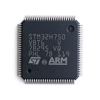
AT32F407VGT7 - 240MHz Cortex-M4 MCU 1MB Flash | Artery
Teilenummer: AT32F407VGT7 ✓ Aktiv| Menge | Stückpreis | Gesamt |
|---|---|---|
| 1 | $3.44 | $3,44 |
| 10 | $3.1 | $31,00 |
| 100 | $2.61 | $261,00 |
| 500 | $2.4 | $1.200,00 |
| 1.000 | $2.33 | $2.330,00 |
AT32F407VGT7 Übersicht
A microcontroller (MCU) is a single-chip computer containing a processor core, program memory (Flash), data memory (SRAM), and a rich set of on-chip peripherals. The Cortex-M4 family targets high-performance embedded applications that require deterministic real-time control, DSP for audio/signal processing, and a single-precision Floating Point Unit (FPU) for efficient math. Within the power-management and embedded hierarchy, this part sits as: Cortex-M4 -> ARMv7-M architecture -> 32-bit MCU -> embedded processor -> semiconductor. The AT32F407 line is engineered by Artery as a cost-effective alternative to mainstream M4 families, with faster core clocks and dual-bank Flash for safer firmware updates.
Key features include 240 MHz core speed, single-precision FPU, DSP extensions, 1 MB Flash (dual-bank option with sLib security library), 224 KB SRAM, three 12-bit ADCs (3 MSPS), two 12-bit DACs, USB 2.0 FS host/device/OTG, 10/100 Ethernet MAC, two CAN 2.0B interfaces, SDIO, FSMC, and up to 17 timers. Communication peripherals include I2C, SPI, I2S, USART and UART, totalling up to 21 communication interfaces. Operating voltage is 2.6 V to 3.6 V with an industrial -40C to +105C junction temperature range.
The architecture combines an M4 core with tightly-coupled SRAM, multi-layer AHB/APB buses, and a DMA controller for low-CPU-overhead data movement. The dual-bank Flash supports in-application programming (IAP) without halting execution, and the sLib security region protects intellectual property. The 240 MHz clock enables deterministic control loops and DSP workloads that are typically out of reach for lower-end MCUs.
Typical applications include industrial motor control (BLDC, FOC drives), USB/Ethernet connected gateways, USB Type-C power-delivery controllers, consumer audio with DSP effects, human-machine interface (HMI) panels with LCD via FSMC, drones/flight controllers, and IoT edge nodes. The combination of CAN, Ethernet and USB makes it well-suited to automotive aftermarket and industrial automation products.
When designing with this MCU, ensure the external quartz or resonator load capacitors match the AT32 reference design (typically 8-20 pF), and place the on-board 1uF/100nF decoupling network within 3 mm of every VDD/VDDA pin. Always configure the option-byte write protection for production units to lock the bootloader region from accidental erase during field updates.
This page synthesises distributor pricing, drop-in alternatives, and practical design notes that complement the manufacturer datasheet DS_AT32F407_V2.04_EN.pdf and the LCSC stock snapshot.
Drop-in-Alternativen für AT32F407VGT7 – gleiches Gehäuse, Pin-kompatibel. Bauteile mit anderem Gehäuse, die eine PCB-Überarbeitung erfordern, sind ausgeschlossen.
Varianten dieser Serie
Modelle derselben Serie, die drop-in-kompatibel sind mit AT32F407VGT7 (gleiche Bauform und Footprint) – abweichend in ADC, Communication Interfaces, Operating Temperature, Package, SRAM.
Schnellvergleichstool – Wählen Sie Alternativbauteile für den Direktvergleich:
AT32F407VGT6
✅ Drop-In ⚠️ Spezifikationen ungeprüft📋 Referenzalternative (nicht im Katalog)
AT32F407RGT7
✅ Drop-In ⚠️ Spezifikationen ungeprüft📋 Referenzalternative (nicht im Katalog)
GD32F407VGT6
✅ Drop-In📋 Referenzalternative (nicht im Katalog)
STM32F407VGT6
✅ Drop-In✓ Auf Lager
$7.55 / Stück
Datenblatt ansehen →APM32F407VGT6
✅ Drop-In📋 Referenzalternative (nicht im Katalog)
AT32F407VGT7 Grenzwerte & elektrische Eigenschaften
| Core Architecture | ARM Cortex-M4 with FPU and DSP |
| Maximum CPU Frequency | 240 MHz |
| Program Flash | 1024 KB (dual-bank with sLib, configurable 256 KB to 1024 KB) |
| SRAM | 224 KB (max, depending on Flash configuration) |
| Operating Voltage | 2.6 V to 3.6 V |
| Gehäuse | LQFP-100 (14x14 mm, 0.5 mm pitch) |
| Betriebstemperatur | -40C to +105C (industrial) |
| ADC | 3x 12-bit, up to 3 MSPS |
| DAC | 2x 12-bit |
| USB | USB 2.0 FS OTG, host/device |
| Ethernet | 10/100 MAC (requires external PHY) |
| CAN | 2x CAN 2.0B |
| Timers | 17 (general-purpose, advanced, basic, system) |
| Communication Interfaces | Up to 21 (USART/UART, I2C, SPI, I2S, USB, CAN, SDIO, FSMC) |
| External Memory Bus | FSMC (8/16-bit, supports LCD) |
| DMA | 2x 7-channel DMA controllers |
| Montageart | Surface Mount |
| Lead-Free / RoHS | Compliant per LCSC product page |
AT32F407VGT7 lqfp-100 (14x14 mm, 0.5 mm pitch) Pinbelegungsleitfaden
Pinbelegung für AT32F407VGT7 (lqfp-100 (14x14 mm, 0.5 mm pitch)-Gehäuse). Dieser digitale IC umfasst GPIO, Kommunikationsschnittstellen (UART, SPI, I2C) und Versorgungspins. Alternative Pin-Funktionen und Konfigurationsoptionen entnehmen Sie dem Herstellerdatenblatt. Unverzichtbar für Embedded-System-Design und PCB-Layout.
Keine detaillierten Pinbelegungsdaten verfügbar für AT32F407VGT7.
Siehe die Datenblatt für die vollständige Pin-Konfiguration.
Typische Anwendungen
AT32F407VGT7 ist geeignet für 6 Anwendungs: Industrial BLDC / FOC Motor Control, USB Type-C Power Delivery (PD) Controller, Industrial IoT Gateway with Ethernet, FPV Flight Controller / Drone, HMI Panel with LCD via FSMC, Consumer Audio DSP Effects Processor.
Industrial BLDC / FOC Motor Control
The AT32F407VGT7's 240 MHz Cortex-M4 with single-precision FPU and three 12-bit 3 MSPS ADCs makes it a strong fit for sensorless Field-Oriented Control (FOC) of BLDC and PMSM motors. The high clock rate lets the inner current loop run at 20-40 kHz while the outer speed loop runs at 4-8 kHz, and the three ADCs synchronise to the advanced timer for sub-microsecond sampling alignment. DSP extensions accelerate Park/Clarke transforms and the SVM calculation that drive the three-phase PWM output. Compared to the STM32F407VGT6's 168 MHz, the AT32 delivers 43% more processing headroom for the same FOC algorithm at a lower unit price.
Empfohlen
USB Type-C Power Delivery (PD) Controller
The integrated USB 2.0 FS OTG controller and 17 timers make the AT32F407VGT7 well suited as a USB Type-C PD source/sink controller. The part can run the PD 3.1 state machine over CC lines using comparator timers and hardware PWM, while the 224 KB SRAM hosts USB-PD protocol stacks with logging. The 240 MHz core processes BMC-encoded messages and source-capability negotiation within tens of microseconds. Dual-bank Flash supports safe firmware updates over USB DFU without bricking chargers in the field.
Empfohlen
Industrial IoT Gateway with Ethernet
The AT32F407VGT7's 10/100 Ethernet MAC (with external PHY) plus USB OTG and CAN 2.0B make it an ideal edge gateway that bridges industrial buses to IP networks. The Cortex-M4 with FPU can run lwIP plus an MQTT/TLS stack at 240 MHz, sustaining 5-10 Mbps throughput. The 224 KB SRAM hosts TCP sockets and TLS handshakes; 1024 KB Flash stores firmware for multiple southbound protocols (Modbus, CANopen). Two CAN controllers and 21 total communication interfaces simplify multi-protocol bridging in factory automation.
Empfohlen
FPV Flight Controller / Drone
The 240 MHz Cortex-M4 with FPU has been adopted in FPV flight controllers because it provides enough throughput to run Betaflight or INAV with 8 kHz gyro loops and 32 kHz motor PWM. The AT32F407VGT7's 17 timers generate DSHOT600/1200 motor protocols, while the three ADCs read battery voltage, current, and analogue RSSI at high update rates. The USB OTG is used for configurator communication, and dual-bank Flash ensures field firmware upgrades are recoverable. Compared to STM32F405-based flight controllers, AT32 variants deliver smoother performance per watt.
Empfohlen
HMI Panel with LCD via FSMC
The FSMC external memory controller on the AT32F407VGT7 drives 8/16-bit parallel LCDs (TN, IPS) without external logic, simplifying HMI designs in industrial appliances and consumer white goods. The 240 MHz core renders fonts and animations smoothly while reading touch coordinates via I2C. With 1024 KB Flash, full Chinese GBK or Unicode tables fit on-chip alongside application code, eliminating the cost of an external SPI Flash. The dual-bank option also enables OTA updates from a remote server.
Empfohlen
Consumer Audio DSP Effects Processor
The Cortex-M4 DSP extensions and single-precision FPU let the AT32F407VGT7 implement real-time audio effects (EQ, reverb, compression) at 48 kHz sample rates across stereo I2S streams. The two 12-bit DACs and I2S interfaces simplify connection to external Class-D amplifiers, while the 17 timers synchronise audio processing to a low-jitter PLL clock. Compared to legacy Cortex-M3 designs, the 240 MHz AT32F407VGT7 typically doubles DSP headroom at a similar price, allowing reverb tails up to 500 ms without CPU saturation.
Empfohlen
Zusammenfassung der empfohlenen Produkte
Technische Referenzdaten für AT32F407VGT7 – Vergleich, Designhinweise und Compliance-Informationen.
Auswahlhilfe
Vergleich mit Alternativen
| Parameter | Dieses Produkt | AT32F407VGT6 | GD32F407VGT6 | STM32F407VGT6 | APM32F407VGT6 |
|---|---|---|---|---|---|
| Brand | Artery | Artery | GigaDevice | STMicroelectronics | Geehy |
| Package | LQFP-100 (14x14 mm) | LQFP-100 (14x14 mm) | LQFP-100 (14x14 mm) | LQFP-100 (14x14 mm) | LQFP-100 (14x14 mm) |
| Core | Cortex-M4F (FPU+DSP) | Cortex-M4F | Cortex-M4F | Cortex-M4F | Cortex-M4F |
| Max Frequency | 240 MHz | 240 MHz | 168 MHz | 168 MHz | 240 MHz |
| Flash | 1024 KB dual-bank | 1024 KB dual-bank | 1024 KB single-bank | 1024 KB single-bank | 1024 KB dual-bank |
| SRAM | 224 KB | 224 KB | 192 KB | 192 KB | 224 KB |
| USB OTG | Yes (FS) | Yes (FS) | Yes (FS) | Yes (FS) | Yes (FS) |
| Ethernet MAC | 10/100 | 10/100 | 10/100 | 10/100 | 10/100 |
Wichtigste Unterscheidungsmerkmale
- Highest CPU clock in the Cortex-M4 LQFP-100 class (vs. STM32F407VGT6)
- Dual-bank Flash with sLib security region (vs. GD32F407VGT6)
- 21 communication interfaces in a single chip (vs. APM32F407VGT6)
Designhinweise
Power the AT32F407VGT7 from a single 3.3 V rail. Place a 10 uF bulk capacitor within 10 mm of the VDD pin cluster, and pair each VDD/VSS pair with a 100 nF X7R 0402/0603 cap. VDDA requires a 10 nH ferrite bead or 10 ohm resistor plus a 100 nF + 1 uF decoupling pair to keep ADC SNR within datasheet spec; this is critical for motor control and instrumentation designs.
Route the HSE crystal traces as short and symmetric as possible, with grounded guard traces and load capacitors (typically 8-20 pF) placed within 2 mm of the OSC_IN/OSC_OUT pins. For LQFP-100 designs use at least 4-layer stack-up with a continuous ground plane beneath the part to provide a low-impedance return path for the high-speed USB and Ethernet signals.
The AT32F407VGT7 boot pins (BOOT0) must be tied to GND through a 10 kohm resistor for normal boot from Flash; floating BOOT0 will intermittently enter System Memory bootloader and confuse production flashing. Always lock the option bytes (including sLib region) before shipping to prevent field misprogramming. Estimated: option-byte lock sequence takes ~200 ms after VDD stabilises.
Compliance-Informationen
RoHS compliance per LCSC product page listing; REACH and halogen-free status not explicitly documented on Artery datasheet excerpt provided.