STM32F407VGT6 - 1MB Flash, 168MHz ARM Cortex-M4 MCU | STMicroelectronics
MPN: STM32F407VGT6 ✓ Active| Qty | Unit Price | Extended |
|---|---|---|
| 1 | $11.45 | $11.45 |
| 10 | $10.35 | $103.50 |
| 100 | $9.2 | $920.00 |
| 500 | $8.3 | $4,150.00 |
| 1,000 | $7.55 | $7,550.00 |
STM32F407VGT6 Overview
What is a microcontroller? A microcontroller (MCU) is a compact integrated circuit that governs a specific operation in an embedded system, combining a processor core, memory, and programmable peripherals on a single chip. The STM32F407VGT6 belongs to the STM32F4 series within the broader STM32 family of ARM Cortex-M microcontrollers, positioned in the high-performance Cortex-M4 segment of the power/performance hierarchy below Cortex-M7 devices such as the STM32F7 and STM32H7.
Key features include the ART Accelerator enabling 0-wait-state Flash execution, a memory protection unit (MPU), 3x 12-bit ADCs, 2x 12-bit DACs, 17 timers including two advanced motor-control timers, and a rich communication set: USART, SPI, I2C, CAN, USB OTG FS/HS, and an Ethernet MAC with IEEE 1588 support. A camera interface (DCMI) and true random number generator (RNG) round out the peripheral portfolio.
Technically, the device operates from a 1.8V to 3.6V supply, with an internal 1.2V core regulator (VCAP bypass), 5V-tolerant I/O pins, and an internal 16 MHz RC oscillator plus external crystal support up to 26 MHz. It is specified from -40C to +85C (industrial grade) and is RoHS compliant.
Typical applications include motor control using the advanced timers and ADCs, audio processing leveraging the FPU and DACs, and industrial automation using CAN and Ethernet. The camera interface also suits embedded vision nodes.
Design tip: ensure adequate decoupling on all VDD pins, provide a clean analog supply for the ADCs, and place the 1.2V bypass capacitors close to the VCAP pins for regulator stability.
This page synthesizes distributor pricing, drop-in alternatives including the GigaDevice GD32F407VGT6, and practical design notes not found in the ST datasheet, providing a comprehensive resource for engineers evaluating the STM32F407VGT6. Prices are as of 2026-09-06.
Drop-in alternatives for STM32F407VGT6 — same package, pin-to-pin compatible. Different-package parts requiring PCB rework are excluded.
Variants in this series
Same-series models that are drop-in compatible with STM32F407VGT6 (same form factor and footprint) — differing in Communication Interfaces, Core, Package, SRAM, Flash Memory.
Quick Comparison Tool — Select alternative parts for side-by-side comparison:
STM32F405VGT6
✅ Drop-In ⚠️ 参数待验证✓ In Stock
$8.1 / Unit
View Datasheet →STM32F415VGT6
✅ Drop-In ⚠️ 参数待验证✓ In Stock
$8.1 / Unit
View Datasheet →STM32F417VGT6
✅ Drop-In ⚠️ 参数待验证✓ In Stock
$8.1 / Unit
View Datasheet →STM32F413VGT6
✅ Drop-In ⚠️ 参数待验证✓ In Stock
$8.1 / Unit
View Datasheet →GD32F407VGT6
✅ Drop-In📋 Reference alternative (not in catalog)
STM32F407VGT6 Maximum Ratings & Electrical Characteristics
| Core | ARM 32-bit Cortex-M4 with FPU |
| Maximum Clock Frequency | 168 MHz |
| Performance | 210 DMIPS / 1.25 DMIPS/MHz |
| Flash Memory | 1 MB |
| SRAM | 192 KB + 4 KB backup SRAM |
| Supply Voltage | 1.8 V to 3.6 V |
| Core Voltage (internal regulator) | 1.2 V |
| Timers | 17 (12 general-purpose, 2 advanced-control) |
| ADC | 3x 12-bit |
| DAC | 2x 12-bit |
| Communication Interfaces | USART, SPI, I2C, CAN, USB OTG FS/HS, Ethernet MAC |
| Camera Interface | Yes (DCMI) |
| True Random Number Generator | Yes |
| I/O Pins | 82 (5V tolerant) |
| Operating Temperature | -40C to +85C |
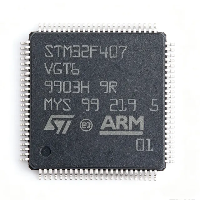
| Package | LQFP-100 (14x14 mm) |
| Mounting Style | SMD/SMT |
| RoHS Status | Compliant |
STM32F407VGT6 Pin Configuration
| Pin 1 | PE2 — Port E I/O |
| Pin 2 | PE3 — Port E I/O |
| Pin 3 | PE4 — Port E I/O |
| Pin 4 | PE5 — Port E I/O |
| Pin 5 | PE6 — Port E I/O |
| Pin 6 | VBAT — Battery backup supply |
| Pin 7 | PC13 — Port C I/O (RTC affine) |
| Pin 8 | PC14-OSC32_IN — Port C I/O / 32.768 kHz oscillator input |
| Pin 9 | PC15-OSC32_OUT — Port C I/O / 32.768 kHz oscillator output |
| Pin 10 | PH0-OSC_IN — Main oscillator input |
| Pin 11 | PH1-OSC_OUT — Main oscillator output |
| Pin 12 | NRST — System reset (active low) |
| Pin 13 | PC0 — Port C I/O / ADC input |
| Pin 14 | PC1 — Port C I/O / ADC input |
| Pin 15 | PC2 — Port C I/O / ADC input |
| Pin 16 | PC3 — Port C I/O / ADC input |
| Pin 17 | VSSA — Analog ground |
| Pin 18 | VREF- — ADC reference low |
| Pin 19 | VREF+ — ADC reference high |
| Pin 20 | VDDA — Analog supply |
| Pin 21 | PA0-WKUP — Port A I/O / wake-up / ADC |
| Pin 22 | PA1 — Port A I/O / ADC |
| Pin 23 | PA2 — Port A I/O / ADC / USART2_TX |
| Pin 24 | PA3 — Port A I/O / ADC / USART2_RX |
| Pin 25 | VSS — Digital ground |
| Pin 26 | VDD — Digital supply |
| Pin 27 | PA4 — Port A I/O / DAC_OUT1 / SPI1_NSS |
| Pin 28 | PA5 — Port A I/O / DAC_OUT2 / SPI1_SCK |
| Pin 29 | PA6 — Port A I/O / SPI1_MISO |
| Pin 30 | PA7 — Port A I/O / SPI1_MOSI |
| Pin 31 | PC4 — Port C I/O / ADC input |
| Pin 32 | PC5 — Port C I/O / ADC input |
| Pin 33 | PB0 — Port B I/O / ADC / VCAP-adjacent I/O |
| Pin 34 | PB1 — Port B I/O / ADC |
| Pin 35 | PB2-BOOT1 — Port B I/O / boot pin 1 |
| Pin 36 | PE7 — Port E I/O / FSMC |
| Pin 37 | PE8 — Port E I/O / FSMC |
| Pin 38 | PE9 — Port E I/O / FSMC |
| Pin 39 | PE10 — Port E I/O / FSMC |
| Pin 40 | PE11 — Port E I/O / FSMC |
| Pin 41 | PE12 — Port E I/O / FSMC |
| Pin 42 | PE13 — Port E I/O / FSMC |
| Pin 43 | PE14 — Port E I/O / FSMC |
| Pin 44 | PE15 — Port E I/O / FSMC |
| Pin 45 | PB10 — Port B I/O / I2C2_SCL / USART3_TX |
| Pin 46 | PB11 — Port B I/O / I2C2_SDA / USART3_RX |
| Pin 47 | VCAP_1 — Internal 1.2V regulator bypass capacitor 1 |
| Pin 48 | VDD — Digital supply |
| Pin 49 | PB12 — Port B I/O / SPI2_NSS / CAN2 |
| Pin 50 | PB13 — Port B I/O / SPI2_SCK / CAN2 |
| Pin 51 | PB14 — Port B I/O / SPI2_MISO / TIM1_CH2N |
| Pin 52 | PB15 — Port B I/O / SPI2_MOSI / TIM1_CH3N |
| Pin 53 | PD8 — Port D I/O / FSMC / USART3_TX |
| Pin 54 | PD9 — Port D I/O / FSMC / USART3_RX |
| Pin 55 | PD10 — Port D I/O / FSMC |
| Pin 56 | PD11 — Port D I/O / FSMC |
| Pin 57 | PD12 — Port D I/O / FSMC / TIM4_CH1 |
| Pin 58 | PD13 — Port D I/O / FSMC / TIM4_CH2 |
| Pin 59 | PD14 — Port D I/O / FSMC / TIM4_CH3 |
| Pin 60 | PD15 — Port D I/O / FSMC / TIM4_CH4 |
| Pin 61 | PC6 — Port C I/O / TIM8_CH1 / SDIO |
| Pin 62 | PC7 — Port C I/O / TIM8_CH2 / SDIO |
| Pin 63 | PC8 — Port C I/O / TIM8_CH3 / SDIO |
| Pin 64 | PC9 — Port C I/O / TIM8_CH4 / SDIO |
| Pin 65 | PA8 — Port A I/O / TIM1_CH1 / MCO1 / ETH |
| Pin 66 | PA9 — Port A I/O / TIM1_CH2 / USART1_TX |
| Pin 67 | PA10 — Port A I/O / TIM1_CH3 / USART1_RX |
| Pin 68 | PA11 — Port A I/O / TIM1_CH4 / USB_DM / CAN1_RX |
| Pin 69 | PA12 — Port A I/O / USB_DP / CAN1_TX |
| Pin 70 | PA13 — Port A I/O / JTMS-SWDIO |
| Pin 71 | VCAP_2 — Internal 1.2V regulator bypass capacitor 2 |
| Pin 72 | VDD — Digital supply |
| Pin 73 | PA14 — Port A I/O / JTCK-SWCLK |
| Pin 74 | PA15 — Port A I/O / JTDI / SPI1_NSS |
| Pin 75 | PC10 — Port C I/O / SDIO / USART3 |
| Pin 76 | PC11 — Port C I/O / SDIO / USART3 |
| Pin 77 | PC12 — Port C I/O / SDIO / UART5_TX |
| Pin 78 | PD0 — Port D I/O / FSMC / CAN1_RX |
| Pin 79 | PD1 — Port D I/O / FSMC / CAN1_TX |
| Pin 80 | PD2 — Port D I/O / SDIO / TIM3_ETR |
| Pin 81 | PD3 — Port D I/O / FSMC / USART2_CTS |
| Pin 82 | PD4 — Port D I/O / FSMC / USART2_RTS |
| Pin 83 | PD5 — Port D I/O / FSMC / USART2_TX |
| Pin 84 | PD6 — Port D I/O / FSMC / USART2_RX |
| Pin 85 | PD7 — Port D I/O / FSMC / USART2_CK |
| Pin 86 | PB3 — Port B I/O / JTDO / SPI1_SCK |
| Pin 87 | PB4 — Port B I/O / NJTRST / SPI1_MISO |
| Pin 88 | PB5 — Port B I/O / SPI1_MOSI / CAN2 |
| Pin 89 | PB6 — Port B I/O / I2C1_SCL / USART1_TX |
| Pin 90 | PB7 — Port B I/O / I2C1_SDA / USART1_RX |
| Pin 91 | BOOT0 — Boot mode select |
| Pin 92 | PB8 — Port B I/O / I2C1_SCL / CAN1_RX |
| Pin 93 | PB9 — Port B I/O / I2C1_SDA / CAN1_TX |
| Pin 94 | VSS — Digital ground |
| Pin 95 | VDD — Digital supply |
| Pin 96 | PE0 — Port E I/O / FSMC |
| Pin 97 | PE1 — Port E I/O / FSMC |
| Pin 98 | VSS — Digital ground |
| Pin 99 | VDD — Digital supply |
| Pin 100 | PDR_ON — Power-down reset enable |
Typical Applications
STM32F407VGT6 is suitable for 6 applications: Industrial Motor Control, Industrial IoT Gateway, Digital Audio Processing, Embedded Vision Node, Test and Measurement Instruments, Home Automation and Smart Devices.
Industrial Motor Control
The STM32F407VGT6 fits motor drives through its two advanced-control timers (TIM1/TIM8) providing complementary PWM with dead-time insertion, and three 12-bit ADCs converting at up to 2.4 Msps for phase-current sensing. The 168 MHz Cortex-M4F with FPU executes field-oriented control (FOC) loops in real time using DSP instructions, while CAN and Ethernet interfaces link the drive to factory automation networks. Placed in the control stage with gate drivers such as the STGAP1AS, it delivers closed-loop speed and torque control for BLDC/PMSM motors; the 5V-tolerant I/O simplifies interfacing with hall sensors and encoder outputs.
Recommended
Industrial IoT Gateway
For IoT gateways, the STM32F407VGT6 combines an Ethernet MAC with IEEE 1588 precision-time support, CAN 2.0B buses for field devices, and USB OTG for local configuration - all integrated on-chip, eliminating an external Ethernet controller. The 1 MB Flash accommodates a TCP/IP stack (LwIP), TLS layers, and OTA bootloader with room to spare; 192 KB SRAM buffers network packets and sensor telemetry. Running FreeRTOS plus LwIP at 168 MHz, the MCU typically sustains line-rate 100 Mbps bridging between CAN/RS-485 sensor clusters and a cloud uplink while staying within a compact LQFP-100 footprint.
Recommended
Digital Audio Processing
The single-precision FPU and DSP instructions of the 168 MHz Cortex-M4F core enable real-time audio effects, filtering, and CODEC control, while the two 12-bit DACs output analog audio directly and I2S interfaces connect external high-resolution codecs. The STM32F407VGT6 sustains multi-band EQ or reverb algorithms with headroom at 48 kHz stereo. Its low-jitter clock tree, derived from an external crystal up to 26 MHz with PLL, meets I2S master-clock accuracy requirements, and USB OTG FS supports USB Audio Class streaming for professional audio peripherals and effects pedals.
Recommended
Embedded Vision Node
The dedicated DCMI camera interface of the STM32F407VGT6 connects parallel-output CMOS image sensors without FPGA assistance, streaming video frames into SRAM via DMA at 168 MHz bandwidth. A QSPI memory interface extends frame buffering beyond internal SRAM, and the FPU accelerates histogram, thresholding, and simple detection algorithms on-frame. Typical designs pair a 2 MP sensor with the DCMI at VGA/QVGA rates for machine-vision inspection, QR reading, or smart-camera applications; the Ethernet MAC then uploads processed results to a host, making a complete single-chip vision endpoint.
Recommended
Test and Measurement Instruments
The STM32F407VGT6 serves as a host controller in handheld scopes, data loggers, and bench instruments, where its three 12-bit ADCs sample at 2.4 Msps, timers provide precise interval measurement, and the FPU handles post-processing math. USB OTG enables PC connectivity and firmware updates, while the 1 MB Flash stores calibration tables, UI assets, and logging firmware. The ART Accelerator guarantees 0-wait-state execution for deterministic interrupt latency - critical for trigger timing - and the true RNG supports security features for instrument authentication and encrypted data export.
Recommended
Home Automation and Smart Devices
Smart panels, thermostats, and security hubs leverage the STM32F407VGT6 for its balance of performance and connectivity: multiple USARTs and I2C handle Zigbee/RS-485 radio modules and sensors, while the RNG and crypto-ready family variants support secure commissioning. The 82 I/O pins in LQFP-100 drive touch keys, relays, and displays from one controller, and the 1 MB Flash accommodates a graphics library plus OTA update capability. Its 5V-tolerant I/O and industrial -40C to +85C rating improve robustness in electrically noisy residential environments.
Recommended
Recommended Products Summary
Engineering reference data for STM32F407VGT6 — comparison, design guidance, and compliance information.
Selection Guide
Comparison with Alternatives
| Parameter | This Product | STM32F405VGT6 | STM32F415VGT6 | STM32F417VGT6 | STM32F413VGT6 | GD32F407VGT6 |
|---|---|---|---|---|---|---|
| Package | LQFP-100 (14x14 mm) | LQFP-100 - same | LQFP-100 - same | LQFP-100 - same | LQFP-100 - same | LQFP-100 - same |
| Brand | STMicroelectronics | STMicroelectronics | STMicroelectronics | STMicroelectronics | STMicroelectronics | GigaDevice |
| Core / Max Frequency | Cortex-M4F, 168 MHz | Cortex-M4F, 168 MHz | Cortex-M4F, 168 MHz | Cortex-M4F, 168 MHz | Cortex-M4F, 100 MHz | Cortex-M4F, 168 MHz |
| Flash Memory | 1 MB | 1 MB | 1 MB | 1 MB | 1.5 MB | 1 MB (2x512 KB banks) |
| SRAM | 192 KB + 4 KB backup | 192 KB + 4 KB backup | 192 KB + 4 KB backup | 192 KB + 4 KB backup | 320 KB + 4 KB backup | 192 KB |
| Ethernet MAC | Yes | No | Yes | Yes | No | Yes |
| Hardware Crypto (AES) | No | No | Yes | Yes | No | No |
| Camera Interface (DCMI) | Yes | Yes | Yes | Yes | Yes | Yes |
| Ecosystem | STM32Cube / HAL / rich ST support | STM32Cube / HAL | STM32Cube / HAL | STM32Cube / HAL | STM32Cube / HAL | GD32 firmware library; partial STM32 HAL compatibility |
Key Differentiators
- Integrated Ethernet MAC with IEEE 1588 (vs STM32F405VGT6)
- Cost-optimized pin-compatible upgrade with crypto (vs STM32F417VGT6)
- Mature ecosystem and supply reliability (vs GD32F407VGT6)
Design Notes
The internal 1.2V core regulator requires 2.2 uF low-ESR ceramic capacitors on both VCAP_1 (pin 47) and VCAP_2 (pin 71), placed within 2 mm of each pin with solid via connections to ground. Per ST hardware development guidance (AN4488), never inject external voltage on VCAP. Decouple all six VDD pins with 100 nF ceramics plus one bulk 4.7 uF per supply rail group; VDDA should be filtered with an ferrite bead and 1 uF + 10 nF network to protect the 12-bit ADC noise floor.
For the Ethernet MAC, route RMII/ref-clock traces as length-matched pairs to a 50 MHz external oscillator or use the MCO output (PA8) feeding the PHY - keep PHY traces under 10 cm with 50-ohm impedance control. USB OTG HS ULPI or FS DP/DM pairs need 90-ohm differential routing. Place the 8 MHz HSE crystal close to PH0/PH1 with guard ground; keep DCMI camera bus (up to 8-bit data plus sync) short and grouped to preserve setup/hold margin at high pixel clocks.
Set BOOT0 (pin 91) to ground via a 10 k resistor for normal Flash boot; floating BOOT0 can cause sporadic entry into the system bootloader. PDR_ON (pin 100) must be tied to VDD for standard power-down reset behavior. Note that Flash sector erase granularity is non-uniform (16/64/128 KB sectors) - place frequent-update parameters in the smallest sectors to reduce wear and update time. When using the internal RTC, provide VBAT (pin 6) backup or tie it to VDD through proper decoupling.
Estimated: at 168 MHz full-speed operation with all peripherals active, the STM32F407VGT6 draws roughly 50-90 mA from 3.3 V, dissipating approximately 0.17-0.30 W. The LQFP-100 theta_JA of about 48 C/W on a standard 4-layer board yields an estimated junction rise of only 8-14 C above ambient - no heatsinking is needed. Ensure ambient stays below the 85 C maximum with margin for adjacent power-stage heating in motor-drive enclosures.
Compliance Information
RoHS compliant and lead-free per STMicroelectronics product data. Industrial temperature grade -40C to +85C. Automotive-qualified variant STM32F407VGT7 exists for AEC-relevant applications.