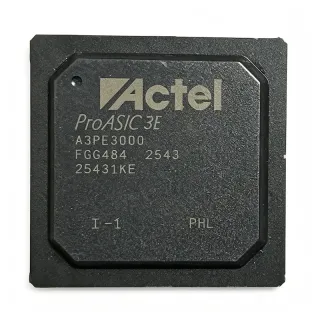
LFE2-20E-6F484C - 21K LUT ECP2 FPGA | Lattice Semiconductor
Teilenummer: LFE2-20E-6F484C ✗ AbgekündigtLFE2-20E-6F484C Übersicht
An FPGA is a semiconductor whose digital logic and connectivity can be configured after manufacture. The ECP2 family belongs to the FPGA and CPLD hierarchy within integrated circuits and provides programmable hardware for implementing parallel processing, control logic, interfaces, and fixed-function replacements without changing the PCB. Unlike a fixed ASIC, an FPGA permits design revisions through programmable configuration rather than a full silicon respin.
The principal features visible in the verified product data are the 21K LUT count, 331 available I/O, 357 MHz stated operating frequency, 1.2 V core voltage, and -6 speed designation. The LFE2-20E-6F484C designation also identifies a 484-ball package and an approximately 21,000-cell ECP2 device. Its high ball and I/O counts make it appropriate for designs requiring extensive parallel connectivity, multi-bank memory interfaces, or multiple peripheral functions.
The device is implemented in 90 nm CMOS and operates from a stated 1.2 V core supply. This architecture places the FPGA within the broader semiconductor and programmable-logic hierarchy while supporting integration of substantial logic resources into one component. Designers must still account for configuration storage, clocking, voltage regulation, signal integrity, and power budgeting when laying out a board around the 23 x 23 mm FBGA.
Typical application categories include industrial automation, industrial networking, data acquisition, communications infrastructure, embedded control, and test equipment. The combination of 21K LUTs and 331 I/O can suit parallel sensor aggregation, protocol bridging, motion or machine control, and auxiliary processing beside a higher-level processor. Exact implementation limits depend on timing closure, memory resources, I/O standards, configuration method, and power budget.
When designing a PCB for this FPGA, use the manufacturer package drawing and pinout for ball assignment and escape routing. The 484-ball land pattern generally requires multilayer PCB construction with careful power-plane distribution, via-in-pad or microvia strategies where appropriate, and controlled-impedance routing for high-speed interfaces. Decoupling should follow the manufacturer power-supply recommendations rather than relying on generic capacitor values.
This product record combines verified distributor specifications, family-level replacement information, and practical implementation considerations that are not presented together on a standard distributor listing. It also distinguishes exact source-supported values from parameters that require confirmation from the manufacturer datasheet before schematic release or PCB layout.
Drop-in-Alternativen für LFE2-20E-6F484C – gleiches Gehäuse, Pin-kompatibel. Bauteile mit anderem Gehäuse, die eine PCB-Überarbeitung erfordern, sind ausgeschlossen.
Varianten dieser Serie
Modelle derselben Serie, die drop-in-kompatibel sind mit LFE2-20E-6F484C (gleiche Bauform und Footprint) – abweichend in Speed Grade, Package, DSP Capability, Logic Cells, Package Type.
LFE2-20E-5F484I
✅ Drop-InPreis auf Anfrage
Datenblatt ansehen →LFE2-20E-5F484C
✅ Drop-In ⚠️ Spezifikationen ungeprüftPreis auf Anfrage
Datenblatt ansehen →LFE2-20E-7F484C
✅ Drop-In ⚠️ Spezifikationen ungeprüftPreis auf Anfrage
Datenblatt ansehen →LFE2-20E-6F484I
✅ Drop-In ⚠️ Spezifikationen ungeprüftPreis auf Anfrage
Datenblatt ansehen →LFE2-20E-7F484I
✅ Drop-In ⚠️ Spezifikationen ungeprüft📋 Referenzalternative (nicht im Katalog)
LFE2-20E-6F484C Grenzwerte & elektrische Eigenschaften
| Device Type | ECP2 Field Programmable Gate Array (FPGA) |
| Logic Cells | 20,000 cells |
| Look-Up Tables | 21K LUTs |
| Maximum Stated Frequency | 357 MHz |
| Core Supply Voltage | 1.2 V |
| Speed Grade | -6 |
| Process Technology | 90 nm CMOS |
| I/O Count | 331 I/O |
| Gehäuse | 484-FBGA |
| Package Type | FPBGA-484 |
| Terminal Count | 484 terminals |
| Package Body Size | 23 x 23 mm |
| Montageart | Surface mount |
LFE2-20E-6F484C 23 x 23 mm Pinbelegungsleitfaden
Pinbelegung für LFE2-20E-6F484C (23 x 23 mm-Gehäuse). Dieser digitale IC umfasst GPIO, Kommunikationsschnittstellen (UART, SPI, I2C) und Versorgungspins. Alternative Pin-Funktionen und Konfigurationsoptionen entnehmen Sie dem Herstellerdatenblatt. Unverzichtbar für Embedded-System-Design und PCB-Layout.

Keine detaillierten Pinbelegungsdaten verfügbar für LFE2-20E-6F484C.
Siehe die Datenblatt für die vollständige Pin-Konfiguration.
Typische Anwendungen
LFE2-20E-6F484C ist geeignet für 6 Anwendungs: Industrial Automation and Machine Control, Industrial Networking and Protocol Bridging, Data Acquisition and Signal Conditioning, Communications Infrastructure Equipment, Embedded Control and Sensor Aggregation, Test and Measurement Equipment.
Industrial Automation and Machine Control
The LFE2-20E-6F484C fits deterministic machine-control logic because it combines 21K LUTs with 331 I/O in a 484-FBGA package. A controller can implement sequencing, interlocks, encoder or sensor interfaces, and communication adaptation in parallel rather than relying entirely on a microcontroller. The 357 MHz stated device frequency provides useful headroom for logic pipelines, but the -6 grade must still be validated through post-layout timing. Industrial designers should confirm the selected temperature option, supported I/O standards, isolation architecture, and functional-safety requirements before releasing the design.
Empfohlen
Industrial Networking and Protocol Bridging
The LFE2-20E-6F484C can serve as a parallel protocol engine or bridge when a system must reconcile multiple fieldbus or serial interfaces. Its 331 I/O provide substantial connectivity, while the 21K LUT class can accommodate framing, buffering, state machines, and test logic. The device is implemented in 90 nm CMOS and operates from a stated 1.2 V core supply. Clock-domain crossings and I/O voltage adaptation must be designed explicitly, because the supplied data does not specify the supported I/O ranges or embedded-memory organization.
Empfohlen
Data Acquisition and Signal Conditioning
For parallel data acquisition, the LFE2-20E-6F484C can combine control sequencing, digital filtering, timestamp logic, and interface coordination in one ECP2 FPGA. Its 21K LUTs and 331 I/O are appropriate for aggregating multiple digital channels, while the 357 MHz stated frequency supports timing-sensitive sampling pipelines. Analog front-end conditioning remains external, and the designer must establish signal-integrity and clocking schemes for each interface. The 484-FBGA package requires a multilayer layout with carefully distributed power and controlled impedance.
Empfohlen
Communications Infrastructure Equipment
The LFE2-20E-6F484C is suitable for line-card, interface, or protocol-processing functions in communications equipment where parallel programmable logic is useful. The 21K LUT and 331-I/O resources can support packet filtering, channel control, aggregation, and test features, while the -6 speed grade targets more demanding timing paths than the -5 option. Designers should separate high-speed serial routing from FPGA fabric, use the manufacturer clocking guidance, and verify transceiver lane requirements. The supplied evidence does not provide the package ball map, so signal assignment must come directly from current Lattice documentation.
Empfohlen
Embedded Control and Sensor Aggregation
The LFE2-20E-6F484C can consolidate sensor conditioning, digital filtering, event detection, and actuator sequencing in embedded industrial or IoT edge equipment. Its 331 I/O offer ample parallel connectivity, and the 21K LUT class supports concurrent logic paths without requiring multiple smaller devices. The 1.2 V core operating point simplifies integration with modern FPGA power architecture, although exact regulator selection depends on unpublished current limits. Critical implementations should confirm operating temperature, I/O tolerances, configuration strategy, and recovery behavior before production release.
Empfohlen
Test and Measurement Equipment
The LFE2-20E-6F484C can implement pattern generation, acquisition sequencing, timing control, and interface orchestration in test equipment. Its 21K LUTs allow parallel test engines, while 331 I/O support dense fixture or backplane connections and the 357 MHz stated frequency supports high-rate digital logic. The 484-FBGA package demands controlled-impedance routing, robust power distribution, and careful clock topology. Before schematic completion, obtain the package drawing, I/O standards, and power-consumption tables because these details are not included in the verified distributor snippets.
Empfohlen
Zusammenfassung der empfohlenen Produkte
Technische Referenzdaten für LFE2-20E-6F484C – Vergleich, Designhinweise und Compliance-Informationen.
Auswahlhilfe
Vergleich mit Alternativen
| Parameter | Dieses Produkt | LFE2-20E-5F484I | LFE2-20E-5F484C | LFE2-20E-7F484C | LFE2-20E-6F484I | LFE2-20E-7F484I |
|---|---|---|---|---|---|---|
| Brand | Lattice Semiconductor | Lattice Semiconductor | Lattice Semiconductor | Lattice Semiconductor | Lattice Semiconductor | Lattice Semiconductor |
| Package | 484-FBGA, 23 x 23 mm | 484-FBGA | 484-FBGA | 484-FBGA | 484-FBGA | 484-FBGA |
| FPGA Family | ECP2 | ECP2 | ECP2 | ECP2 | ECP2 | ECP2 |
| Speed Grade | -6 | -5 | -5 | -7 | -6 | -7 |
| Logic Resources | 21K LUTs; 20,000 cells | ECP2 20K-cell class | ECP2 20K-cell class | ECP2 20K-cell class | ECP2 20K-cell class | ECP2 20K-cell class |
| Process Technology | 90 nm CMOS | 90 nm CMOS | 90 nm CMOS | 90 nm CMOS | 90 nm CMOS | 90 nm CMOS |
Wichtigste Unterscheidungsmerkmale
- Faster speed-grade option than the -5 replacement (vs. LFE2-20E-5F484I)
- Lower-grade timing alternative remains available in the same footprint (vs. LFE2-20E-5F484C)
- Higher timing headroom than the same-family -6 option (vs. LFE2-20E-6F484I)
- High connectivity for parallel programmable logic (vs. LFE2-20E-7F484C)
Designhinweise
Treat the 484-FBGA footprint as a high-density, multilayer layout problem rather than a conventional two-layer component. Use the current Lattice package drawing and exact ball map before defining vias, pad stacks, or escape routing. Reserve continuous ground and core-supply planes, distribute decoupling close to the relevant supply balls, and avoid splitting planes beneath the device. The verified package dimensions are 23 x 23 mm, but those dimensions alone do not determine whether a specific via-in-pad or microvia process is required.
Design the 1.2 V core rail around the actual switching activity of the final ECP2 design rather than a generic FPGA-current estimate. Separate the FPGA core from other load groups so switching regulators and digital loads do not inject noise into the supply. Place the manufacturer-recommended bulk and high-frequency capacitors at the associated power and ground balls, then verify voltage droop at the package with an oscilloscope. The supplied records do not publish current limits, tolerance, sequencing, or decoupling values, so those items must come from the current Lattice power guidelines.
Preserve controlled impedance and return paths for every high-speed interface, and avoid crossing power or split-ground boundaries with critical traces. The -6 speed grade and 357 MHz stated device frequency do not mean every I/O can operate at 357 MHz; each interface has separate timing and I/O-standard constraints. Use the Lattice timing analyzer for internal fabric paths and the applicable board-level signal-integrity guidance for external interfaces. Configuration lines, clocks, resets, and JTAG should also be planned with appropriate termination or pull arrangements shown in the verified schematic guidance.
Do not infer full drop-in interchangeability from the ECP2 family name or the 484-ball suffix alone. Verify the order code, speed grade, temperature suffix, package drawing, configuration interface, and I/O map for every proposed substitution. The cross-reference search expressly warns that package and speed differences can prevent interchangeability. Before schematic release, compare the target and replacement against the manufacturer ordering guide and run an equivalence check on every power, ground, configuration, clock, and user I/O ball.
Compliance-Informationen
The supplied distributor and datasheet-index search results do not explicitly state RoHS, REACH, AEC-Q100, lead-free, halogen-free, or conflict-minerals status. These fields remain unknown pending the current manufacturer product page or declaration.