Lattice Semiconductor

LFE2-20E-6F484C - 21K LUT ECP2 FPGA | Lattice Semiconductor

Référence : LFE2-20E-6F484C ✗ Fin de vie
1.2 V Vdss 484-FBGA Package 357 MHz Speed
MOQ : 1 |

LFE2-20E-6F484C Présentation

Lattice Semiconductor LFE2-20E-6F484C is an ECP2 field-programmable gate array with 21K LUTs, 331 I/O, a 357 MHz stated maximum frequency, and a 1.2 V supply in a 484-FBGA package. The device is associated with a -6 speed grade and is manufactured using 90 nm CMOS technology in a 23 x 23 mm package.

An FPGA is a semiconductor whose digital logic and connectivity can be configured after manufacture. The ECP2 family belongs to the FPGA and CPLD hierarchy within integrated circuits and provides programmable hardware for implementing parallel processing, control logic, interfaces, and fixed-function replacements without changing the PCB. Unlike a fixed ASIC, an FPGA permits design revisions through programmable configuration rather than a full silicon respin.

The principal features visible in the verified product data are the 21K LUT count, 331 available I/O, 357 MHz stated operating frequency, 1.2 V core voltage, and -6 speed designation. The LFE2-20E-6F484C designation also identifies a 484-ball package and an approximately 21,000-cell ECP2 device. Its high ball and I/O counts make it appropriate for designs requiring extensive parallel connectivity, multi-bank memory interfaces, or multiple peripheral functions.

The device is implemented in 90 nm CMOS and operates from a stated 1.2 V core supply. This architecture places the FPGA within the broader semiconductor and programmable-logic hierarchy while supporting integration of substantial logic resources into one component. Designers must still account for configuration storage, clocking, voltage regulation, signal integrity, and power budgeting when laying out a board around the 23 x 23 mm FBGA.

Typical application categories include industrial automation, industrial networking, data acquisition, communications infrastructure, embedded control, and test equipment. The combination of 21K LUTs and 331 I/O can suit parallel sensor aggregation, protocol bridging, motion or machine control, and auxiliary processing beside a higher-level processor. Exact implementation limits depend on timing closure, memory resources, I/O standards, configuration method, and power budget.

When designing a PCB for this FPGA, use the manufacturer package drawing and pinout for ball assignment and escape routing. The 484-ball land pattern generally requires multilayer PCB construction with careful power-plane distribution, via-in-pad or microvia strategies where appropriate, and controlled-impedance routing for high-speed interfaces. Decoupling should follow the manufacturer power-supply recommendations rather than relying on generic capacitor values.

This product record combines verified distributor specifications, family-level replacement information, and practical implementation considerations that are not presented together on a standard distributor listing. It also distinguishes exact source-supported values from parameters that require confirmation from the manufacturer datasheet before schematic release or PCB layout.

Alternatives de remplacement direct pour LFE2-20E-6F484C — même boîtier, compatible broche à broche. Les références à boîtier différent nécessitant une retouche du PCB sont exclues.

Variantes de cette série

Modèles de la même série directement compatibles avec LFE2-20E-6F484C (même facteur de forme et même empreinte) — différant par Speed Grade, Package, DSP Capability, Logic Cells, Package Type.

Lattice Semiconductor
Speed Grade: -5
Package: 484-BBGA
DSP Capability: DSP
Comparer avec LFE2-20E-6F484C →
Lattice Semiconductor
Logic Cells: 21,000 cells
Comparer avec LFE2-20E-6F484C →
Lattice Semiconductor
Speed Grade: -7
Package: 484-BBGA
DSP Capability: DSP blocks present
Comparer avec LFE2-20E-6F484C →

LFE2-20E-5F484I

✅ Remplacement direct
Lattice Semiconductor
📦 FBGA-484
Field-Programmable Gate Array (FPGA) · LatticeECP2 · 21,000 cells · 21K LUTs · 331 I/O · Yes · 1.2 V · -5

Contactez-nous pour le prix

Voir la fiche technique →

LFE2-20E-5F484C

✅ Remplacement direct ⚠️ Spécifications non vérifiées
Lattice Semiconductor
📦 FBGA-484
ECP2 Field Programmable Gate Array (FPGA) · 21K LUTs · 331 I/O · 1.2 V · -5 · DSP · 484-BBGA · BGA

Contactez-nous pour le prix

Voir la fiche technique →

LFE2-20E-7F484C

✅ Remplacement direct ⚠️ Spécifications non vérifiées
Lattice Semiconductor
📦 FBGA-484
ECP2 Field Programmable Gate Array (FPGA) · 21,000 LUTs · 331 I/O · DSP blocks present · 1.2 V · -7 · 484-BBGA · Surface Mount

Contactez-nous pour le prix

Voir la fiche technique →

LFE2-20E-6F484I

✅ Remplacement direct ⚠️ Spécifications non vérifiées
Lattice Semiconductor
📦 FBGA-484
ECP2 Field Programmable Gate Array (FPGA) · 21,000 cells · 2,625 LABs · 21K LUTs · 331 I/O · 331 DSP · 282,624 bits · 1.2 V

Contactez-nous pour le prix

Voir la fiche technique →

LFE2-20E-7F484I

✅ Remplacement direct ⚠️ Spécifications non vérifiées
📦 FBGA-484
Same ECP2 20K-cell family and 484-ball package, with a -7 speed grade that is 16.7% higher than the target -6 speed designation and an I ordering suffix.

📋 Alternative de référence (hors catalogue)

LFE2-20E-6F484C Valeurs maximales et caractéristiques électriques

Device Type ECP2 Field Programmable Gate Array (FPGA)
Logic Cells 20,000 cells
Look-Up Tables 21K LUTs
Maximum Stated Frequency 357 MHz
Core Supply Voltage 1.2 V
Speed Grade -6
Process Technology 90 nm CMOS
I/O Count 331 I/O
Boîtier 484-FBGA
Package Type FPBGA-484
Terminal Count 484 terminals
Package Body Size 23 x 23 mm
Type de montage Surface mount

Guide de configuration des broches du LFE2-20E-6F484C 23 x 23 mm

Configuration des broches du LFE2-20E-6F484C (boîtier 23 x 23 mm). Ce circuit intégré numérique comprend des GPIO, des interfaces de communication (UART, SPI, I2C) et des broches d'alimentation. Consultez la fiche technique du fabricant pour les fonctions alternatives des broches et les options de configuration. Indispensable pour la conception de systèmes embarqués et la conception de circuits imprimés.

Schéma de brochage du boîtier 23 x 23 mm pour le LFE2-20E-6F484C

Aucune donnée de brochage détaillée disponible pour LFE2-20E-6F484C.

Consultez la fiche technique pour la configuration complète des broches.

Applications typiques

LFE2-20E-6F484C convient pour 6 applications: Industrial Automation and Machine Control, Industrial Networking and Protocol Bridging, Data Acquisition and Signal Conditioning, Communications Infrastructure Equipment, Embedded Control and Sensor Aggregation, Test and Measurement Equipment.

🏭

Industrial Automation and Machine Control

The LFE2-20E-6F484C fits deterministic machine-control logic because it combines 21K LUTs with 331 I/O in a 484-FBGA package. A controller can implement sequencing, interlocks, encoder or sensor interfaces, and communication adaptation in parallel rather than relying entirely on a microcontroller. The 357 MHz stated device frequency provides useful headroom for logic pipelines, but the -6 grade must still be validated through post-layout timing. Industrial designers should confirm the selected temperature option, supported I/O standards, isolation architecture, and functional-safety requirements before releasing the design.

🌐

Industrial Networking and Protocol Bridging

The LFE2-20E-6F484C can serve as a parallel protocol engine or bridge when a system must reconcile multiple fieldbus or serial interfaces. Its 331 I/O provide substantial connectivity, while the 21K LUT class can accommodate framing, buffering, state machines, and test logic. The device is implemented in 90 nm CMOS and operates from a stated 1.2 V core supply. Clock-domain crossings and I/O voltage adaptation must be designed explicitly, because the supplied data does not specify the supported I/O ranges or embedded-memory organization.

📡

Data Acquisition and Signal Conditioning

For parallel data acquisition, the LFE2-20E-6F484C can combine control sequencing, digital filtering, timestamp logic, and interface coordination in one ECP2 FPGA. Its 21K LUTs and 331 I/O are appropriate for aggregating multiple digital channels, while the 357 MHz stated frequency supports timing-sensitive sampling pipelines. Analog front-end conditioning remains external, and the designer must establish signal-integrity and clocking schemes for each interface. The 484-FBGA package requires a multilayer layout with carefully distributed power and controlled impedance.

🌐

Communications Infrastructure Equipment

The LFE2-20E-6F484C is suitable for line-card, interface, or protocol-processing functions in communications equipment where parallel programmable logic is useful. The 21K LUT and 331-I/O resources can support packet filtering, channel control, aggregation, and test features, while the -6 speed grade targets more demanding timing paths than the -5 option. Designers should separate high-speed serial routing from FPGA fabric, use the manufacturer clocking guidance, and verify transceiver lane requirements. The supplied evidence does not provide the package ball map, so signal assignment must come directly from current Lattice documentation.

🧩

Embedded Control and Sensor Aggregation

The LFE2-20E-6F484C can consolidate sensor conditioning, digital filtering, event detection, and actuator sequencing in embedded industrial or IoT edge equipment. Its 331 I/O offer ample parallel connectivity, and the 21K LUT class supports concurrent logic paths without requiring multiple smaller devices. The 1.2 V core operating point simplifies integration with modern FPGA power architecture, although exact regulator selection depends on unpublished current limits. Critical implementations should confirm operating temperature, I/O tolerances, configuration strategy, and recovery behavior before production release.

🖥️

Test and Measurement Equipment

The LFE2-20E-6F484C can implement pattern generation, acquisition sequencing, timing control, and interface orchestration in test equipment. Its 21K LUTs allow parallel test engines, while 331 I/O support dense fixture or backplane connections and the 357 MHz stated frequency supports high-rate digital logic. The 484-FBGA package demands controlled-impedance routing, robust power distribution, and careful clock topology. Before schematic completion, obtain the package drawing, I/O standards, and power-consumption tables because these details are not included in the verified distributor snippets.

What are the key specifications of LFE2-20E-6F484C that engineers should know?
The LFE2-20E-6F484C is a 21K-LUT ECP2 FPGA with 331 I/O, a 357 MHz stated maximum frequency, a 1.2 V core supply, and a 484-FBGA package. According to the verified DigiKey and Mouser product records, it uses 90 nm CMOS and is packaged in a 23 x 23 mm FPBGA-484. These figures position it as a medium-density programmable-logic device for parallel control, communications, data acquisition, and industrial equipment. Final timing and resource conclusions still depend on the selected design, speed grade, I/O standards, and clocking requirements.
Where can I buy LFE2-20E-6F484C online?
LFE2-20E-6F484C is listed by DigiKey, Mouser, Octopart, DiGi-Electronics, and several authorized or independent distributors. The verified DigiKey result identifies the Lattice Semiconductor Corporation as the manufacturer and shows the part as an ECP2 FPGA with 331 I/O in a 484-BBGA package, while the DiGi-Electronics listing explicitly reports in-stock inventory. Exact unit pricing and XAIPART fulfillment terms were not included in the source data as of 2026-10-30, so a current distributor quote should be requested before purchasing.
What is the price of LFE2-20E-6F484C?
A verified numerical price for LFE2-20E-6F484C was not published in the supplied search results as of 2026-10-30. The results confirm that DigiKey, Mouser, Octopart, DiGi-Electronics, and other distributors list the device, and DiGi-Electronics reports it in stock, but no exact tier prices are available to reproduce reliably. Price can vary with quantity, date, authorized-distributor inventory, and traceability requirements. The pricing fields in this record therefore use 0.00 as an unavailable-price placeholder rather than presenting an invented commercial quotation.
What is the lead time for LFE2-20F6F484C?
The verified lead time for LFE2-20E-6F484C is not available as a numerical value as of 2026-10-30. DiGi-Electronics describes the component as in stock with fast delivery, while DigiKey states that it ships today; those statements indicate available inventory but do not establish a guaranteed factory lead time for larger quantities. For production planning, request a written quotation covering the required quantity, date code, package condition, and traceability. The verified manufacturer identity is Lattice Semiconductor Corporation.
Is LFE2-20E-6F484C in stock?
LFE2-20E-6F484C is reported in stock by the verified DiGi-Electronics product page as of 2026-10-30, and DigiKey and Mouser provide ordering links for the same manufacturer part number. This confirms marketplace availability for at least some sellers, but it does not prove XAIPART inventory or a guaranteed allocation for a specific production quantity. Wolfchip also reported 20,375 pieces in stock in its search result, although its update was dated 2026-02-25. Buyers should therefore confirm current stock, lead time, and date-code traceability before placing an order.
LFE2-20E-6F484C vs LFE2-20E-5F484C — which is better for a timing-critical design?
LFE2-20E-6F484C is generally the better choice when the design needs the faster -6 grade rather than the -5 grade of LFE2-20E-5F484C. Both are ECP2 devices identified with the same 20K-cell family, 21K-LUT resource class, 1.2 V core supply, and 484-ball package in the supplied comparison data. The exact timing margin must be checked with the Lattice timing analyzer and the complete design constraints. The -6 designation is approximately 20% higher in the underlying speed-grade number than -5, although it does not guarantee a proportional increase in every design’s achievable frequency.
What is the difference between LFE2-20E-6F484C and LFE2-20SE-6F484I?
LFE2-20E-6F484C and LFE2-20SE-6F484I are both ECP2 484-ball options, but their ordering codes indicate different family features and temperature grades. The supplied Findchips comparison explicitly associates LFE2-20SE-6F484I with the target, while the target record identifies a 357 MHz stated maximum, 1.2 V core voltage, and -6 speed grade. Because pin-level compatibility and the exact meaning of the SE suffix are not established by the supplied snippets, engineers should compare the manufacturer ordering guide, package drawings, and I/O tables before treating the part as a drop-in replacement.
When should I choose LFE2-20E-6F484C over LFE2-20E-5F484I?
Choose LFE2-20E-6F484C when the design’s timing closure is better served by the -6 speed grade, and choose LFE2-20E-5F484I when lower cost or supply favors the slower grade. Both parts belong to the same ECP2 20K-cell class with 1.2 V operation and a 484-ball package, so either can serve parallel logic designs with 331 I/O. The selection should be based on the worst-path timing report, available inventory, and required operating-temperature grade rather than the suffix alone. A design close to its timing limit should retain the faster grade until post-layout timing is complete.
Is LFE2-20E-6F484C suitable for industrial automation and control systems?
Yes, LFE2-20E-6F484C is suitable for industrial automation and control systems when its 21K LUTs, 331 I/O, and 357 MHz stated frequency satisfy the design. The ECP2 architecture can implement deterministic parallel control, protocol conversion, data collection, and machine-control functions in a single programmable device. Industrial suitability must also be confirmed against the exact operating-temperature grade, supported I/O standards, isolation requirements, and long-term availability. The supplied search snippets do not state the operating-temperature range, so that parameter remains marked as data needed.
What can replace LFE2-20E-6F484C on the same 484-ball footprint?
The verified ECP2 comparison data supports reviewing LFE2-20E-5F484I as a same-family, same-package replacement candidate, while several speed- and temperature-grade ordering options can also be evaluated from the same Lattice family. Compatibility still requires confirmation of the package drawing, ball map, configuration interface, I/O standards, voltage requirements, and timing grade. The provided cross-reference sources explicitly caution that family membership does not establish interchangeability. No cross-brand drop-in replacement was verified, so changing manufacturers may require a PCB redesign or a detailed pin-to-pin equivalence review.
Is LFE2-20E-6F484C the same as LFE2-20E-6FN484C?
No equivalence should be assumed solely because LFE2-20E-6FN484C appears in the ECP2 comparison results. The verified FindIC record identifies both as 484-pin ECP2 devices with 21,000 cells, 90 nm CMOS, and a 1.2 V core voltage, but it explicitly warns that their main parameters and circuit structures may differ and that modification may be required for replacement. Engineers should compare the complete Lattice ordering guide, package suffix definitions, I/O map, and pinout before using the FN484C version in an existing LFE2-20E-6F484C design.
Where can I download the LFE2-20E-6F484C datasheet PDF?
The verified LFE2-20E-6F484C datasheet PDF is accessible through the FindIC product page at https://www.findic.us/price/lfe2-20e-6f484c-me6Gk7yYz.html. The page identifies the device as a 357 MHz, 20,000-cell ECP2 FPGA in a 23 x 23 mm FPBGA-484 package and links to a published PDF. Distributor listings from DigiKey and Mouser also provide datasheet navigation. For design release, obtain the current Lattice ECP2 family documentation and package drawings because an archived or distributor-hosted PDF may not represent the latest revision.
Where can I find the LFE2-20E-6F484C pinout and ball assignment?
The authoritative LFE2-20E-6F484C ball assignment is found in the Lattice ECP2 family documentation and the package drawing for the 484-FBGA device. The verified product records establish that this is a 484-terminal, 23 x 23 mm FPBGA-484 package with ball terminals, but they do not include the individual signal names for all 484 balls. Consequently, this record does not reproduce a potentially inaccurate 484-entry pin table. Before PCB layout, download the current manufacturer pinout, verify the package suffix, and use the exact ball map associated with LFE2-20E-6F484C.
What power and decoupling requirements apply to LFE2-20E-6F484C?
LFE2-20E-6F484C uses a stated 1.2 V core supply, but the verified snippets do not provide current limits, permitted voltage tolerance, power coefficients, decoupling values, or external regulator requirements. Those values must be taken from the current manufacturer datasheet and the power estimator for the selected design. In implementation, reserve a continuous, low-impedance power plane, place bulk and high-frequency decoupling according to the manufacturer recommendation, and isolate noisy switching supplies from sensitive FPGA rails. Package thermal and power calculations should use actual configuration activity rather than a theoretical worst case alone.
Is there a best cross-brand equivalent for LFE2-20E-6F484C?
No verified best cross-brand equivalent was found for LFE2-20E-6F484C in the supplied alternative search results. The results identify same-brand ECP2 candidates such as LFE2-20E-5F484I and LFE2-20SE-6F484I, but a cross-manufacturer substitute would require equivalence of the 484-ball footprint, 1.2 V core supply, I/O standards, configuration method, memory resources, and timing architecture. Generic search tools identify potential FPGA substitutes but do not prove drop-in compatibility. A direct manufacturer-to-manufacturer migration should therefore be treated as a new design effort unless Lattice and the alternative manufacturer publish a verified pin-equivalence matrix.

Données de référence d'ingénierie pour LFE2-20E-6F484C — comparaison, recommandations de conception et informations de conformité.

Guide de sélection

Choose LFE2-20E-6F484C when a design needs the ECP2 20K-cell resource class, 331 I/O, 1.2 V operation, and a 484-FBGA package with a -6 speed designation. Select LFE2-20E-5F484I or LFE2-20E-5F484C when supply or cost favors the slower -5 grade and post-layout timing confirms adequate margin. LFE2-20E-6F484I is the closest reviewed same-speed ordering alternative, subject to verification of its temperature suffix and exact I/O map. LFE2-20E-7F484C and LFE2-20E-7F484I provide a 16.7% higher speed-grade number, but cost, availability, power, and timing must still be evaluated. No cross-brand drop-in replacement was verified, so a migration to another FPGA manufacturer should be treated as a design conversion rather than a routine substitution.

Comparaison avec les alternatives

Paramètre Ce produit LFE2-20E-5F484I LFE2-20E-5F484C LFE2-20E-7F484C LFE2-20E-6F484I LFE2-20E-7F484I
Brand Lattice Semiconductor Lattice Semiconductor Lattice Semiconductor Lattice Semiconductor Lattice Semiconductor Lattice Semiconductor
Package 484-FBGA, 23 x 23 mm 484-FBGA 484-FBGA 484-FBGA 484-FBGA 484-FBGA
FPGA Family ECP2 ECP2 ECP2 ECP2 ECP2 ECP2
Speed Grade -6 -5 -5 -7 -6 -7
Logic Resources 21K LUTs; 20,000 cells ECP2 20K-cell class ECP2 20K-cell class ECP2 20K-cell class ECP2 20K-cell class ECP2 20K-cell class
Process Technology 90 nm CMOS 90 nm CMOS 90 nm CMOS 90 nm CMOS 90 nm CMOS 90 nm CMOS

Principaux différenciateurs

  • Faster speed-grade option than the -5 replacement (vs LFE2-20E-5F484I)
  • Lower-grade timing alternative remains available in the same footprint (vs LFE2-20E-5F484C)
  • Higher timing headroom than the same-family -6 option (vs LFE2-20E-6F484I)
  • High connectivity for parallel programmable logic (vs LFE2-20E-7F484C)

Notes de conception

Treat the 484-FBGA footprint as a high-density, multilayer layout problem rather than a conventional two-layer component. Use the current Lattice package drawing and exact ball map before defining vias, pad stacks, or escape routing. Reserve continuous ground and core-supply planes, distribute decoupling close to the relevant supply balls, and avoid splitting planes beneath the device. The verified package dimensions are 23 x 23 mm, but those dimensions alone do not determine whether a specific via-in-pad or microvia process is required.

Design the 1.2 V core rail around the actual switching activity of the final ECP2 design rather than a generic FPGA-current estimate. Separate the FPGA core from other load groups so switching regulators and digital loads do not inject noise into the supply. Place the manufacturer-recommended bulk and high-frequency capacitors at the associated power and ground balls, then verify voltage droop at the package with an oscilloscope. The supplied records do not publish current limits, tolerance, sequencing, or decoupling values, so those items must come from the current Lattice power guidelines.

Preserve controlled impedance and return paths for every high-speed interface, and avoid crossing power or split-ground boundaries with critical traces. The -6 speed grade and 357 MHz stated device frequency do not mean every I/O can operate at 357 MHz; each interface has separate timing and I/O-standard constraints. Use the Lattice timing analyzer for internal fabric paths and the applicable board-level signal-integrity guidance for external interfaces. Configuration lines, clocks, resets, and JTAG should also be planned with appropriate termination or pull arrangements shown in the verified schematic guidance.

Do not infer full drop-in interchangeability from the ECP2 family name or the 484-ball suffix alone. Verify the order code, speed grade, temperature suffix, package drawing, configuration interface, and I/O map for every proposed substitution. The cross-reference search expressly warns that package and speed differences can prevent interchangeability. Before schematic release, compare the target and replacement against the manufacturer ordering guide and run an equivalence check on every power, ground, configuration, clock, and user I/O ball.

Informations de conformité

RoHS
Unknown
REACH
Unknown
AEC-Q100
Unknown
Sans plomb
Unknown
Sans halogène
Unknown
Minerais de conflit
Unknown

The supplied distributor and datasheet-index search results do not explicitly state RoHS, REACH, AEC-Q100, lead-free, halogen-free, or conflict-minerals status. These fields remain unknown pending the current manufacturer product page or declaration.

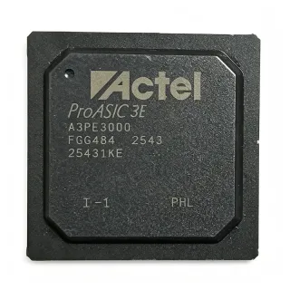
Données vérifiées le : 2026-10-30 — données vérifiées et sélectionnées par l'équipe d'ingénierie composants de XAIPART

Recherches associées

LFE2-20E-6F484C LFE2-20E-6F484C datasheet Lattice Semiconductor LFE2-20E-6F484C LFE2-20E-6F484C 21K LUT 331 I/O LFE2-20E-6F484C 484 FBGA LFE2-20E-6F484C 1.2V FPGA LFE2-20E-6F484C pinout LFE2-20E-6F484C vs LFE2-20E-5F484I LFE2-20E-6F484C drop-in replacement LFE2-20E-6F484C price LFE2-20E-6F484C buy online LFE2-20E-6F484C industrial control FPGA LFE2-20E-6F484C lead time What can replace LFE2-20E-6F484C? Is LFE2-20E-6F484C the same as LFE2-20SE-6F484I?

Composants & termes associés

Lattice Semiconductor LFE2-20E-6F484C LFE2-20E-5F484I LFE2-20E-5F484C LFE2-20E-7F484C LFE2-20E-6F484I LFE2-20E-7F484I ECP2 FPGA CPLD field-programmable gate array programmable logic integrated circuit semiconductor 21K LUTs 20,000 logic cells 331 I/O 357 MHz 1.2 V core supply -6 speed grade 90 nm CMOS 484-FBGA FPBGA-484 surface mount industrial automation industrial networking signal integrity controlled impedance RoHS REACH AEC-Q100
RFQ de devis rapide
Renseignez tous les détails — notre équipe commerciale vous répondra sous 24 heures
Référence Fabricant Boîtier QTY Prix cible Total
✓
Devis envoyé !

Nous répondrons à votre e-mail sous 24 heures

1
RFQ envoyée
2
Devis reçu
3
Commande passée
4
Paiement
5
Expédié
6
Livré
Voir les détails de la RFQ