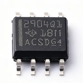
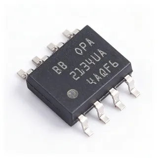
OPA2171AIDR - Dual 36V 3MHz Low-Power Op Amp | Texas Instruments
Teilenummer: OPA2171AIDR ✓ Aktiv| Menge | Stückpreis | Gesamt |
|---|---|---|
| 1 | $0.92 | $0,92 |
| 10 | $0.78 | $7,80 |
| 100 | $0.6 | $60,00 |
| 500 | $0.48 | $240,00 |
| 1.000 | $0.38 | $380,00 |
OPA2171AIDR Übersicht
An operational amplifier (op amp) is a high-gain DC-coupled electronic voltage amplifier with differential inputs and a single-ended output. It is the fundamental building block of analog signal chains, used for amplification, filtering, comparison, buffering, and mathematical operations. The OPA2171 belongs to the lineage of low-power, general-purpose amplifiers, sitting between precision op amps (high accuracy, high power) and high-speed op amps (wide bandwidth, higher noise), optimized for applications requiring moderate bandwidth and low current draw.
Key features of the OPA2171AIDR include 3MHz gain-bandwidth product, 1.5V/µs slew rate, low quiescent current, rail-to-rail output swing, and 36V maximum supply voltage. The 3MHz gain-bandwidth product enables stable operation in active filter circuits, sensor signal conditioning, and transducer amplification. The wide supply range supports industrial 24V bus systems, automotive 12V rails (post-protection), and battery-powered portable equipment operating down to 2.7V.
The OPA2171 uses a CMOS input stage for low input bias current, paired with a rail-to-rail output stage that maximizes dynamic range on low-voltage supplies. Internal EMI/RFI filtering on the inputs improves robustness in harsh electrical environments. The dual op-amp configuration in the SOIC-8 package provides two independent amplifiers in a small footprint, enabling compact multi-channel designs.
Typical applications include transducer amplification, sensor signal conditioning, industrial process control, battery-powered instrumentation, active filters, and voltage reference buffers. The wide input range allows direct interfacing with 24V industrial sensors, while the rail-to-rail output maximizes dynamic range on 3.3V or 5V ADC rails.
When designing with this device, pay attention to input common-mode range, especially near the negative rail where CMOS input stages exhibit degraded behavior. Decouple supply pins with 0.1µF ceramic capacitors placed close to the IC.
This page synthesizes distributor pricing, drop-in alternatives (including same-brand OPA2171AID and OPA4171 variants), and practical design notes not found in the manufacturer datasheet alone.
Drop-in-Alternativen für OPA2171AIDR – gleiches Gehäuse, Pin-kompatibel. Bauteile mit anderem Gehäuse, die eine PCB-Überarbeitung erfordern, sind ausgeschlossen.
Schnellvergleichstool – Wählen Sie Alternativbauteile für den Direktvergleich:
OPA2171AID
✅ Drop-In📋 Referenzalternative (nicht im Katalog)
OPA2191IDR
✅ Drop-In📋 Referenzalternative (nicht im Katalog)
OPA2333AIDR
✅ Drop-In📋 Referenzalternative (nicht im Katalog)
OPA2171AIDR Grenzwerte & elektrische Eigenschaften
| Number of Channels | 2 (Dual) |
| Amplifier Type | General Purpose, Low Power |
| Gain-Bandwidth Product | 3 MHz |
| Slew Rate | 1.5 V/µs |
| Supply Voltage Range (Single) | 2.7 V to 36 V |
| Supply Voltage Range (Dual) | ±1.35 V to ±18 V |
| Ausgangstyp | Rail-to-Rail |
| Input Type | CMOS |
| Betriebstemperaturbereich | -40 °C to +125 °C |
| Gehäuse | SOIC-8 (D) |
| Montageart | Surface Mount |
| MSL-Level | 2 |
| RoHS-Status | Compliant |
OPA2171AIDR Pin-Konfiguration
| Pin 1 | OUTA — Output of amplifier A |
| Pin 2 | INA- — Inverting input of amplifier A |
| Pin 3 | INA+ — Non-inverting input of amplifier A |
| Pin 4 | V- — Negative supply (or ground for single supply) |
| Pin 5 | INB+ — Non-inverting input of amplifier B |
| Pin 6 | INB- — Inverting input of amplifier B |
| Pin 7 | OUTB — Output of amplifier B |
| Pin 8 | V+ — Positive supply |
Typische Anwendungen
OPA2171AIDR ist geeignet für 6 Anwendungs: Industrial 24V Sensor Signal Conditioning, Battery-Powered Portable Instrumentation, Active Filter and Anti-Aliasing Stage, Transducer Amplifier and Bridge Buffer, Voltage and Current Loop Buffers, Power-Supply Voltage and Current Monitor.
Industrial 24V Sensor Signal Conditioning
The OPA2171AIDR's 2.7V to 36V single-supply range and 3 MHz bandwidth suit it to amplifying and filtering signals from industrial 24V-loop-powered sensors including pressure transducers, load cells, and 4-20 mA current loops. Two amplifiers per package enable compact differential-to-single-ended conversion plus gain stage in a single SOIC-8. CMOS inputs keep input bias current in the pA range, so high-impedance sensor bridges are not loaded. Rail-to-rail outputs maximize dynamic range when digitizing on a 5V or 3.3V ADC. Add input protection (Zener/TVS) for harsh industrial transients. Overall, the part offers a cost-effective two-amplifier solution for analog front-ends in PLCs and process-control instrumentation.
Empfohlen
Battery-Powered Portable Instrumentation
Wide 2.7V to 36V supply flexibility and moderate quiescent draw make the OPA2171AIDR suitable for handheld battery-powered test gear where the same board operates from 2x AA cells, USB 5V, or external 24V supplies. Each channel provides 3 MHz GBP, sufficient for audio-bandwidth instrumentation amplifiers and active filters under 100 kHz. Rail-to-rail output swing maximizes ADC range on low-voltage supplies. Two amplifiers per IC economize board space in compact multimeters or data loggers. The SOIC-8 footprint is also easy to hand-prototype and rework. Designers should add a small reverse-battery Schottky for field use and bulk decoupling for motor/relay noise immunity.
Empfohlen
Active Filter and Anti-Aliasing Stage
The OPA2171AIDR's 3 MHz gain-bandwidth product and 1.5 V/µs slew rate are well matched to Sallen-Key or multiple-feedback active low-pass filters with cutoffs up to 200 kHz at low gain. Its rail-to-rail output drives SAR ADCs cleanly without headroom concerns, and CMOS inputs keep filter-component impedance from interacting with bias current. Two amplifiers per package allow second-order filter + ADC buffer or two simultaneous filter channels in one IC. For anti-aliasing ahead of a 100 kS/s ADC, a 50 kHz Butterworth can be implemented with 10 kHz-100 kHz resistor choices. Phase margin is unity-gain stable, so simple buffer configurations need no compensation.
Empfohlen
Transducer Amplifier and Bridge Buffer
Strain-gauge bridge outputs are typically 1-10 mV/V and benefit from a low-offset, low-bias-current instrumentation front end. The OPA2171AIDR provides two CMOS-input amplifiers for INA-style configurations: one INA and one buffer/reference, all in a SOIC-8. The 36V supply allows direct connection to industrial excitation rails, and rail-to-rail output maximizes resolution on a 3.3V or 5V ADC. Although not lowest-offset, the part offers compelling cost for sub-1%-accurate bridge readings in weighing scales, pressure transducers, and force-sensing applications. Match resistor pairs (0.1% preferred) to control common-mode-rejection; add input R-C filtering for ESD and RFI.
Empfohlen
Voltage and Current Loop Buffers
The OPA2171AIDR is well suited as a unity-gain buffer on 4-20 mA current-loop outputs and on 0-10V analog output stages, where it provides low-impedance drive to downstream PLC analog inputs. Wide supply (36V max) lets the buffer operate from a 24V loop supply with headroom for transient protection. Rail-to-rail output means the loop can swing closer to 0V than with non-RRO parts, increasing usable range. Two channels per IC economize space in multi-loop PLCs and process controllers. Add a small output resistor (10-100 ohm) for cable-driver stability and back-EMF protection; ESD clamps at the connector safeguard the IC during field installation.
Empfohlen
Power-Supply Voltage and Current Monitor
Two amplifiers in one SOIC-8 let the OPA2171AIDR implement rail voltage and current monitoring on a single IC. Channel A buffers a high-side current-sense amp output to an ADC; Channel B scales and buffers a 24V rail voltage to a 3.3V ADC. The 36V supply capability is comfortable for a 24V system rail with margin. Rail-to-rail output maximizes dynamic range on the ADC. CMOS inputs reduce loading of high-impedance dividers and current-sense resistors. Use 1% divider resistors for accuracy, and consider a small RC filter on the sense-amp output to reject switching noise. Suitable for server, telecom, and industrial 24V/48V monitoring.
Empfohlen
Zusammenfassung der empfohlenen Produkte
Technische Referenzdaten für OPA2171AIDR – Vergleich, Designhinweise und Compliance-Informationen.
Auswahlhilfe
Vergleich mit Alternativen
| Parameter | Dieses Produkt | OPA2171AID | OPA2191IDR | OPA2333AIDR |
|---|---|---|---|---|
| Brand | Texas Instruments | Texas Instruments | Texas Instruments | Texas Instruments |
| Package | SOIC-8 (D) | SOIC-8 (D) - same | SOIC-8 (D) - same | SOIC-8 (D) - same |
| Number of Channels | 2 | 2 | 2 | 2 |
| Gain-Bandwidth Product | 3 MHz | 3 MHz | 2.5 MHz | 350 kHz |
| Slew Rate | 1.5 V/µs | 1.5 V/µs | 1.5 V/µs | 0.5 V/µs |
| Supply Voltage Range (Single) | 2.7 V to 36 V | 2.7 V to 36 V | 4.5 V to 36 V | 1.8 V to 5.5 V |
| Output Type | Rail-to-Rail | Rail-to-Rail | Rail-to-Rail (RRIO) | Rail-to-Rail (RRIO) |
| Automotive Grade | No (industrial) | No | No | Yes (AEC-Q100, OPA2333AIDR variant) |
| Approx. 1k Price (USD) | $0.38 | $0.38 (tube version) | $0.95 (higher-precision upcharge) | $1.40 (precision upcharge) |
Wichtigste Unterscheidungsmerkmale
- Wider supply voltage than most general-purpose dual op amps (vs. MCP6022-I/SN (Microchip))
- Higher bandwidth and lower cost than precision-grade alternatives (vs. OPA2333AIDR)
- Pin-compatible upgrade path to precision tier (vs. OPA2191IDR)
Designhinweise
Place 0.1µF ceramic supply-decoupling capacitors as close as possible to the V+ and V- pins (Pin 8 and Pin 4 in SOIC-8). Keep ground return paths short and direct; use a continuous ground plane on at least one PCB layer. Avoid routing high-current or high-frequency digital signals adjacent to the op-amp inputs and feedback traces to prevent noise coupling.
Although the OPA2171AIDR is rated to 36V absolute maximum, do not operate continuously at the maximum supply under high ambient temperature. Estimated safe continuous supply is 32V at 85°C ambient. Internal ESD clamps protect against brief overvoltage but not sustained over-voltage; add external TVS protection when interfacing with industrial or automotive transients exceeding 36V.
CMOS inputs exhibit higher bias current (and poorer low-side input common-mode behavior) than JFET inputs when VIN is within ~1.5V of V+. Keep input common-mode voltage at least 1.5V below V+ for linear operation. For unity-gain buffers on high-side signals, add a small pull-up resistor to bias the input above ground if the signal can dip to V-.
Do not rely on the SOIC-8 thermal pad (pin 4) as a heatsink at high power dissipation — the package does not have a thermal pad. Estimated maximum continuous dissipation at 25°C is approximately 600mW (per JEDEC 4-layer board) before derating. For designs operating from 36V with output near mid-rail, current per channel should not exceed ~5mA. If higher current is needed, choose a part with a thermal pad such as the MSOP-10 PowerPAD variant.
Compliance-Informationen
OPA2171AIDR is RoHS-compliant per TI product page. No automotive-grade 'Q1' suffix on this part; for automotive use consider the OPA2171-Q1 family or alternative AEC-Q100 parts. Industrial grade (no AEC-Q100).