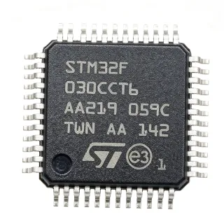
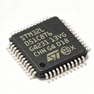
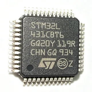
STM32L151CCT6TR - 256KB Flash Cortex-M3 MCU LQFP-48 | STMicroelectronics
Teilenummer: STM32L151CCT6TR ✓ Aktiv| Menge | Stückpreis | Gesamt |
|---|---|---|
| 1 | $7.2 | $7,20 |
| 10 | $6.46 | $64,60 |
| 100 | $5.74 | $574,00 |
| 500 | $5.13 | $2.565,00 |
| 1.000 | $4.58 | $4.580,00 |
| 2.500 | $4.1 | $10.250,00 |
STM32L151CCT6TR Übersicht
An ARM Cortex-M3 microcontroller is a 32-bit RISC processor core designed for embedded applications, balancing deterministic interrupt response, Thumb-2 instruction efficiency, and a rich peripheral ecosystem. The STM32L151CCT6 belongs to the STM32L1 ultra-low-power family: STM32L1 MCU -> ARM Cortex-M MCU -> 32-bit microcontroller -> embedded MCU -> semiconductor IC. Compared with legacy 8-bit or 16-bit microcontrollers, Cortex-M3 devices deliver higher code density, hardware divide, integrated DMA, and standardized CMSIS firmware libraries. The 'L' classification emphasizes dynamic voltage scaling and multiple low-power modes that allow battery-powered designs to operate for years on a single cell.
Key features include a wide 1.65 V to 3.6 V supply range, 7 low-power modes (including a 4.4 uA Stop mode with RTC retention), an integrated LCD controller with built-in voltage booster, a 12-bit ADC with up to 1 Msps, two DACs, and a USB Full-Speed device/host/OTG transceiver with internal pull-up. The two on-chip rail-to-rail op-amps can drive ADC inputs or be used for power management loops, offloading external analog components. Hardware AES 128-bit encryption is included for secure firmware update and data protection.
Architecture is built on the Cortex-M3 core with ST's proprietary ART Accelerator prefetch buffer and a multi-voltage I/O ring that allows the I/O voltage to be set independently of the core supply. The device integrates a brown-out reset (BOR) in Stop mode, a programmable voltage detector (PVD), two independent watchdogs, and a real-time clock with calendar and alarm. Internal oscillators (16 MHz HSI and 37 kHz LSI) reduce external component count, while the 4 MHz MSI RC oscillator is automatically trimmed against the LSE crystal for accurate timing during Sleep and Run modes.
Typical applications include battery-powered sensor nodes, wearable health monitors, energy-harvesting devices, smart meters, industrial sensor transmitters, USB Human Interface Devices (HIDs), and portable medical diagnostic instruments where standby current is measured in microamps and operating current must remain under 10 mA for weeks of autonomy. The integrated op-amps also suit low-side current sensing in motor control and e-bike torque pedals.
Designers should note that the LQFP-48 (7x7 mm) package leaves approximately 4 mm2 of exposed pad-free copper per side, and Pin 1 is the top-left indicator on the tape orientation. A 4-layer PCB with a continuous ground pour is strongly recommended for digital noise immunity and to keep the USB DP/DM traces at 90 ohm differential impedance.
This page synthesizes ST datasheet specifications, distributor pricing snapshots, pin-compatible alternatives drawn from the STM32L1 family, and practical design notes not found in the manufacturer reference manual alone.
Drop-in-Alternativen für STM32L151CCT6TR – gleiches Gehäuse, Pin-kompatibel. Bauteile mit anderem Gehäuse, die eine PCB-Überarbeitung erfordern, sind ausgeschlossen.
Varianten dieser Serie
Modelle derselben Serie, die drop-in-kompatibel sind mit STM32L151CCT6TR (gleiche Bauform und Footprint) – abweichend in Package, Core Architecture, Operational Amplifiers, EEPROM, ADC.
Schnellvergleichstool – Wählen Sie Alternativbauteile für den Direktvergleich:
STM32L152CCT6
✅ Drop-In📋 Referenzalternative (nicht im Katalog)
STM32L151CCT6
✅ Drop-In✓ Auf Lager
$5.2 / Stück
Datenblatt ansehen →STM32L151RCT6
✅ Drop-In ⚠️ Spezifikationen ungeprüft✓ Auf Lager
$3.85 / Stück
Datenblatt ansehen →STM32L152CCT6TR
✅ Drop-In📋 Referenzalternative (nicht im Katalog)
STM32L100CCT6
✅ Drop-In📋 Referenzalternative (nicht im Katalog)
STM32L151C8U6
✅ Drop-In ⚠️ Spezifikationen ungeprüft📋 Referenzalternative (nicht im Katalog)
STM32L151CCT6TR Grenzwerte & elektrische Eigenschaften
| Core Architecture | ARM Cortex-M3 32-bit RISC |
| Maximum CPU Clock | 32 MHz |
| Flash Memory | 256 KB |
| SRAM | 32 KB |
| EEPROM | 8 KB |
| Supply Voltage Range | 1.65 V to 3.6 V |
| Betriebstemperaturbereich | -40 C to +85 C |
| Gehäuse | LQFP-48 (7x7 mm) |
| Montageart | Surface Mount |
| Number of I/Os | 37 |
| USB Interface | USB 2.0 Full-Speed (device/host/OTG) |
| ADC Channels | 14 (12-bit, up to 1 Msps) |
| DAC Channels | 2 (12-bit) |
| Operational Amplifiers | 2 (on-chip rail-to-rail) |
| Low-Power Stop Mode Current | 4.4 uA (typ, with RTC retention) |
| Hardware AES Engine | AES-128 (yes) |
| RoHS-Status | Compliant |
STM32L151CCT6TR Pin-Konfiguration
| Pin 1 | VDD — Power supply |
| Pin 2 | OSC_IN — External oscillator input |
| Pin 3 | OSC_OUT — External oscillator output |
| Pin 4 | NRST — Reset (active low) |
| Pin 5 | VSSA — Analog ground |
| Pin 6 | VDDA — Analog power supply |
| Pin 7 | PA0 — GPIO PA0 / ADC_IN0 |
| Pin 8 | PA1 — GPIO PA1 / ADC_IN1 / OPAMP1_VINP |
| Pin 9 | PA2 — GPIO PA2 / ADC_IN2 / USART2_TX |
| Pin 10 | PA3 — GPIO PA3 / ADC_IN3 / OPAMP1_VINM |
| Pin 11 | PA4 — GPIO PA4 / ADC_IN4 / DAC_OUT1 |
| Pin 12 | PA5 — GPIO PA5 / ADC_IN5 / DAC_OUT2 |
| Pin 13 | PA6 — GPIO PA6 / ADC_IN6 / SP1_MISO |
| Pin 14 | PA7 — GPIO PA7 / ADC_IN7 / SP1_MOSI |
| Pin 15 | PB0 — GPIO PB0 / ADC_IN8 |
| Pin 16 | PB1 — GPIO PB1 / ADC_IN9 |
| Pin 17 | PB2 — GPIO PB2 / BOOT1 |
| Pin 18 | VSS — Digital ground |
| Pin 19 | VDD — Power supply |
| Pin 20 | PB10 — GPIO PB10 / I2C2_SCL |
| Pin 21 | PB11 — GPIO PB11 / I2C2_SDA |
| Pin 22 | PB12 — GPIO PB12 / SPI2_NSS |
| Pin 23 | PB13 — GPIO PB13 / SPI2_SCK |
| Pin 24 | PB14 — GPIO PB14 / SPI2_MISO |
| Pin 25 | PB15 — GPIO PB15 / SPI2_MOSI |
| Pin 26 | PC13 — GPIO PC13 / RTC_TAMP1 |
| Pin 27 | PC14 — GPIO PC14 / OSC32_IN |
| Pin 28 | PC15 — GPIO PC15 / OSC32_OUT |
| Pin 29 | VSS — Digital ground |
| Pin 30 | VDD — Power supply |
| Pin 31 | PH0 — GPIO PH0 / OSC_IN (high-speed crystal) |
| Pin 32 | PH1 — GPIO PH1 / OSC_OUT (high-speed crystal) |
| Pin 33 | PA8 — GPIO PA8 / USART1_CK |
| Pin 34 | PA9 — GPIO PA9 / USART1_TX / OPAMP1_VOUT |
| Pin 35 | PA10 — GPIO PA10 / USART1_RX / OPAMP2_VOUT |
| Pin 36 | PA11 — GPIO PA11 / CAN_RX / USB_DM |
| Pin 37 | PA12 — GPIO PA12 / CAN_TX / USB_DP |
| Pin 38 | PA13 — GPIO PA13 / TMS (SWDIO) |
| Pin 39 | VSS — Digital ground |
| Pin 40 | VDD — Power supply |
| Pin 41 | PA14 — GPIO PA14 / TCK (SWCLK) |
| Pin 42 | PA15 — GPIO PA15 / JTDI / TIM2_CH1 |
| Pin 43 | PB3 — GPIO PB3 / JTDO / TIM2_CH2 |
| Pin 44 | PB4 — GPIO PB4 / JNTRST |
| Pin 45 | PB5 — GPIO PB5 / I2C1_SMBAI |
| Pin 46 | PB6 — GPIO PB6 / I2C1_SCL |
| Pin 47 | PB7 — GPIO PB7 / I2C1_SDA |
| Pin 48 | BOOT0 — Boot mode selection |
Typische Anwendungen
STM32L151CCT6TR ist geeignet für 7 Anwendungs: Battery-Powered IoT Sensor Node, Wearable Health Monitor, USB HID Peripheral Device, Industrial Sensor Transmitter, Smart Electricity Meter, Portable Medical Diagnostic Instrument, Energy-Harvesting Wireless Switch.
Battery-Powered IoT Sensor Node
The STM32L151CCT6TR's 4.4 uA Stop mode with RTC retention and 1.65 V minimum supply make it ideal for long-life IoT sensor nodes. The 256 KB Flash supports Thread/Matter or LoRaWAN MAC libraries with margin, while the integrated 12-bit ADC and dual rail-to-rail op-amps handle sensor conditioning without external analog ICs. At a measured awake current below 10 mA and a duty cycle of one transmit per 60 s, a single 2400 mAh Li-SOCl2 primary cell can power a sensor node for 5 to 10 years.
Empfohlen
Wearable Health Monitor
The device's two on-chip rail-to-rail op-amps can directly amplify ECG, PPG, or GSR sensor signals before the 12-bit ADC, eliminating the need for a separate analog front-end in compact wearable designs. Power consumption in Run mode at 32 MHz remains under 10 mA per the ST datasheet, and the wide 1.65 V to 3.6 V supply range supports direct USB Li-ion recharge integration. Hardware AES-128 enables HIPAA-compliant encrypted storage of patient health records in on-chip Flash.
Empfohlen
USB HID Peripheral Device
The integrated USB 2.0 Full-Speed controller with on-chip pull-up resistor lets the STM32L151CCT6TR connect to a host PC without external USB PHY circuitry, simplifying HID peripherals such as keyboards, mice, barcode scanners, and industrial programmers. At 32 MHz the Cortex-M3 cores serve USB polling endpoints with ample margin for HID report processing, while the Stop mode draws only microwatts during host suspend events. The LQFP-48 package accommodates the required DP/DM trace routing on a 2-layer PCB.
Empfohlen
Industrial Sensor Transmitter
The 4-20 mA current loop or wireless HART sensor transmitter benefits from the wide 1.65 V to 3.6 V input that allows direct connection to 24 V loop power through a low-cost switching regulator. The hardware AES-128 engine secures HART-7 protocol communications while the dual op-amps directly drive 4-20 mA output stages, allowing a two-chip implementation. The LQFP-48 industrial-temperature grade of -40 C to +85 C covers most process and pipeline environments without derating.
Empfohlen
Smart Electricity Meter
The two integrated op-amps perform current-sensing signal conditioning for class-1 metering accuracy without external analog ICs, while the 32 KB SRAM buffers ADC sample bursts. The hardware AES-128 engine secures DLMS/COSEM protocol exchanges per IEC 62056-46, and the integrated LCD segment driver (on STM32L152 equivalents) or 32 GPIO lines drive character displays. Battery backup of RTC at 4.4 uA typical Stop mode meets 10-year retention requirements for unattended electricity meters.
Empfohlen
Portable Medical Diagnostic Instrument
The wide 1.65 V to 3.6 V supply supports direct operation from two AA alkaline cells while the Stop mode retains RTC and tamper-detection logic. The 32 MHz Cortex-M3 core and 256 KB Flash accommodate USB CDC/ECG firmware plus signal-processing libraries, and the integrated 12-bit ADC with up to 1 Msps captures ECG waveforms without an external ADC. The hardware AES-128 supports HIPAA-compliant patient data encryption per FDA cybersecurity guidance.
Empfohlen
Energy-Harvesting Wireless Switch
The 1.65 V minimum supply is compatible with energy-harvested supply rails from piezoelectric switches or solar cells, and the 4.4 uA Stop mode current allows operation from a single BLE packet transmit event. The hardware AES-128 encrypts communication packets, while the 256 KB Flash supports Sub-GHz radio firmware and bidirectional mesh protocols. The integrated op-amps can be configured as ultra-low-power comparators for wake-on-energy detection, eliminating external components.
Empfohlen
Zusammenfassung der empfohlenen Produkte
Technische Referenzdaten für STM32L151CCT6TR – Vergleich, Designhinweise und Compliance-Informationen.
Auswahlhilfe
Vergleich mit Alternativen
| Parameter | Dieses Produkt | STM32L152CCT6 | STM32L151CCT6 | STM32L100CCT6 |
|---|---|---|---|---|
| Brand | STMicroelectronics | STMicroelectronics | STMicroelectronics | STMicroelectronics |
| Package | LQFP-48 (7x7 mm) | LQFP-48 (7x7 mm) - same | LQFP-48 (7x7 mm) - same | LQFP-48 (7x7 mm) - same |
| Core | ARM Cortex-M3 32 MHz | ARM Cortex-M3 32 MHz | ARM Cortex-M3 32 MHz | ARM Cortex-M3 32 MHz |
| Flash | 256 KB | 256 KB | 256 KB | 256 KB |
| USB | USB 2.0 Full-Speed | USB 2.0 Full-Speed | USB 2.0 Full-Speed | No USB |
| Op-Amps | 2 on-chip | 2 on-chip | 2 on-chip | None |
| LCD Controller | No | Yes (4x52 segments) | No | No |
| AES-128 | Yes | Yes | Yes | Yes |
| Stop Mode Current | 4.4 uA typ | 4.4 uA typ | 4.4 uA typ | 4.4 uA typ |
| Packaging | Tape and Reel (TR) | Tray | Tray | Tray |
Wichtigste Unterscheidungsmerkmale
- Only STM32L1 variant with USB AND dual op-amps in LQFP-48 (vs. STM32L100CCT6)
- Hardware AES-128 included for secure communications (vs. STM32F103Z)
- 256 KB Flash at lowest power vs STM32F1 mainstream family (vs. STM32F103Z)
Designhinweise
Place a 100 nF decoupling capacitor directly between each VDD/VSS pin pair and a 4.7 uF bulk capacitor near the VDDA pin. The Stop mode current of 4.4 uA typ only holds when the LSE crystal is enabled for RTC retention; disabling all clocks draws sub-1 uA in Standby mode, per the ST datasheet. Use a separate analog supply rail for VDDA when driving the on-chip op-amps at high source impedances above 100 kohm to preserve ADC SNR.
Route USB DP and DM as a 90 ohm differential pair on the top layer with continuous reference ground beneath, matching the USB 2.0 Full-Speed specification. Keep trace length under 50 mm and minimize vias to one per line. The LQFP-48 (7x7 mm) package exposed pad is not present; run a 4-layer stack with one full ground plane and one power plane to maintain signal integrity across the 32 MHz ARM Cortex-M3 clock traces.
Do not enable the on-chip pull-up resistor on the USB DP pin and also add an external 1.5 kohm pull-up, as the parallel combination violates the USB signal rise/fall timing budget. Always strap BOOT0 to ground through a 10 kohm resistor for normal Flash boot; pulling BOOT0 high at reset enters the system memory bootloader. The NRST pin requires a 100 nF bypass capacitor and an optional external pull-up of 10 kohm to VDD for noisy environments.
At 32 MHz Cortex-M3 operation with all peripherals enabled, the device dissipates up to 144 mW from a 3.3 V supply, well below the LQFP-48 thermal resistance of approximately 95 C/W theta JA. Estimated: junction temperature rise at 25 C ambient is approximately 14 C, confirming no heatsink is required for typical embedded designs. However, the on-chip op-amps can drive 50 mA continuous output and add 0.5 W dissipation if the output stage is shorted; ensure output current limiters are configured.
Compliance-Informationen
RoHS and REACH compliant per ST product page; commercial-grade (-40 C to +85 C) only, not AEC-Q100 qualified. Choose STM32L151RCT6 in extended grade if AEC-Q100 is required for automotive designs.