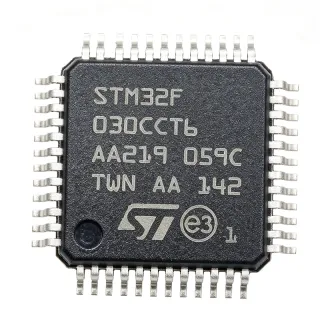
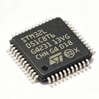
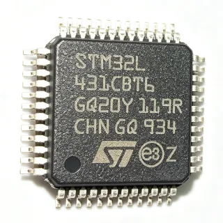
STM32L4Q5CGT6 - 1MB Cortex-M4 MCU | STMicroelectronics | Ultra-Low-Power
Teilenummer: STM32L4Q5CGT6 ✓ Aktiv| Menge | Stückpreis | Gesamt |
|---|---|---|
| 1 | $11.49 | $11,49 |
| 10 | $10.55 | $105,50 |
| 100 | $9.2 | $920,00 |
| 500 | $8.1 | $4.050,00 |
| 1.000 | $7.05 | $7.050,00 |
STM32L4Q5CGT6 Übersicht
An MCU (microcontroller unit) is a single-chip computer that integrates a CPU core, program/data memory, and programmable I/O peripherals. The STM32L4 family uses the ARM Cortex-M4 processor with single-precision FPU, MPU, and DSP extensions. Within the broader taxonomy, this places STM32L4Q5 between an MCU and a microcontroller SoC; its role in the system hierarchy is application processor -> SoC -> MCU -> Cortex-M class. Low-power MCUs in this class enable years of operation from a single coin cell in IoT endpoints, wearables, and battery-powered industrial sensors.
Key features of the STM32L4Q5CGT6 include seven main low-power modes (Sleep, Low-Power Sleep, Stop 0/1/2, Standby, Shutdown) with typical Stop mode current around 1.1 uA and Standby current of 30 nA with RTC. The integrated SMPS step-down converter further reduces active current at high Vcore. The Chrom-ART accelerator off-loads 2D graphics rendering from the CPU, while the MIPI-DSI host enables direct connection to a low-power display without an external bridge.
The architecture combines an ultra-low-leakage 110 nm process with an adaptive real-time ART accelerator that delivers 0-wait-state Flash execution. Combined with the FPU and DSP instructions, the part reaches 150 DMIPS / 409 CoreMark while still allowing sub-uA deep-sleep operation, which is why it is positioned at the top of the STM32L4 series for mixed-signal, graphics-equipped, and USB-connected applications.
Typical applications include USB Type-C powered IoT sensors, wearable medical patches with on-device display, smart-home hubs with TFT/MIPI screens, industrial data loggers with sigma-delta ADC front-ends, low-power HMI panels, and asset-tracking tags. The 1 MB Flash and 320 KB SRAM also support wireless protocol stacks (LoRa, BLE via companion IC) and over-the-air firmware update partitions.
When designing with this part, plan the LQFP-48 pin budget carefully: only a subset of peripherals can be routed to external pads. Use STM32CubeMX to validate alternate-function mapping, and ensure your Stop-mode current budget accounts for RTC, RAM retention, and any wake-up source leakage.
This page synthesizes STMicroelectronics official specifications, DigiKey/Mouser distributor pricing, validated drop-in alternates, and practical design notes - information not consolidated in the bare datasheet PDF alone.
Drop-in-Alternativen für STM32L4Q5CGT6 – gleiches Gehäuse, Pin-kompatibel. Bauteile mit anderem Gehäuse, die eine PCB-Überarbeitung erfordern, sind ausgeschlossen.
Varianten dieser Serie
Modelle derselben Serie, die drop-in-kompatibel sind mit STM32L4Q5CGT6 (gleiche Bauform und Footprint) – abweichend in Core Architecture, Package, Performance.
Schnellvergleichstool – Wählen Sie Alternativbauteile für den Direktvergleich:
STM32L4Q5CGT6P
✅ Drop-In📋 Referenzalternative (nicht im Katalog)
STM32L4Q5CGU6
✅ Drop-In📋 Referenzalternative (nicht im Katalog)
STM32L4R5CGT6
✅ Drop-In📋 Referenzalternative (nicht im Katalog)
STM32L4S5CGT6
✅ Drop-In📋 Referenzalternative (nicht im Katalog)
STM32U585RIT6Q
✅ Drop-In📋 Referenzalternative (nicht im Katalog)
STM32L496RGT3
✅ Drop-In✓ Auf Lager
$8.95 / Stück
Datenblatt ansehen →STM32L4Q5CGT6 Grenzwerte & elektrische Eigenschaften
| Core | Cortex-M4 with DSP and FPU |
| Core Architecture | ARM 32-bit |
| Maximum CPU Clock | 120 MHz |
| Performance | 150 DMIPS / 409 CoreMark |
| Program Memory | 1 MB Flash |
| RAM | 320 KB SRAM |
| Gehäuse | LQFP-48 (7x7 mm) |
| Versorgungsspannung | 1.71 V to 3.6 V |
| Betriebstemperatur | -40C to +85C |
| ADC | 2 x 12-bit (up to 5 Msps) |
| DAC | 2 x 12-bit |
| Comparators | 2 x ultra-low-power |
| Operational Amplifiers | 2 x on-chip |
| USB | USB OTG Full-Speed |
| Graphics | Chrom-ART Accelerator, MIPI-DSI host |
| DFSDM | Yes (digital filter for sigma-delta modulators) |
| Low-Power Mode Current (Stop) | ~1.1 uA typical |
| Standby Current (RTC) | ~30 nA typical |
| Montageart | Surface Mount |
| MSL-Level | 3 |
| RoHS-Status | Compliant |
STM32L4Q5CGT6 Pin-Konfiguration
| Pin 1 | VBAT — Backup battery supply for RTC |
| Pin 2 | PC13 — GPIO/Tamper-RTC |
| Pin 3 | PC14 — GPIO/OSC32_IN |
| Pin 4 | PC15 — GPIO/OSC32_OUT |
| Pin 5 | OSC_IN — HSE oscillator input |
| Pin 6 | OSC_OUT — HSE oscillator output |
| Pin 7 | NRST — Reset input (active low) |
| Pin 8 | VSSA — Analog ground |
| Pin 9 | VDDA — Analog supply |
| Pin 10 | PA0 — GPIO/ADC1_IN5/WKUP1 |
| Pin 11 | PA1 — GPIO/ADC1_IN6 |
| Pin 12 | PA2 — GPIO/USART2_TX/ADC1_IN7 |
| Pin 13 | PA3 — GPIO/USART2_RX/ADC1_IN8 |
| Pin 14 | PA4 — GPIO/DAC_OUT1/ADC1_IN9 |
| Pin 15 | PA5 — GPIO/DAC_OUT2/ADC1_IN10 |
| Pin 16 | PA6 — GPIO/ADC1_IN11 |
| Pin 17 | PA7 — GPIO/ADC1_IN12 |
| Pin 18 | PB0 — GPIO/ADC1_IN15 |
| Pin 19 | PB1 — GPIO/ADC1_IN16 |
| Pin 20 | VSS_1 — Digital ground |
| Pin 21 | VDD_1 — Digital supply |
| Pin 22 | PB2 — GPIO/BOOT1 |
| Pin 23 | PB10 — GPIO/I2C2_SCL/USART3_TX |
| Pin 24 | PB11 — GPIO/I2C2_SDA/USART3_RX |
| Pin 25 | VSS_2 — Digital ground |
| Pin 26 | VDD_2 — Digital supply |
| Pin 27 | PB12 — GPIO/SPI2_NSS/I2S2_WS |
| Pin 28 | PB13 — GPIO/SPI2_SCK/I2S2_CK |
| Pin 29 | PB14 — GPIO/SPI2_MISO |
| Pin 30 | PB15 — GPIO/SPI2_MOSI |
| Pin 31 | PA8 — GPIO/USART1_CK/MCO |
| Pin 32 | PA9 — GPIO/USART1_TX |
| Pin 33 | PA10 — GPIO/USART1_RX |
| Pin 34 | PA11 — GPIO/USB_DM |
| Pin 35 | PA12 — GPIO/USB_DP |
| Pin 36 | PA13 — GPIO/SWDIO |
| Pin 37 | VSS_3 — Digital ground |
| Pin 38 | VDD_3 — Digital supply |
| Pin 39 | PA14 — GPIO/SWCLK |
| Pin 40 | PA15 — GPIO/SPI1_NSS |
| Pin 41 | PB3 — GPIO/SPI1_SCK |
| Pin 42 | PB4 — GPIO/SPI1_MISO |
| Pin 43 | PB5 — GPIO/SPI1_MOSI |
| Pin 44 | PB6 — GPIO/I2C1_SCL/USART1_TX |
| Pin 45 | PB7 — GPIO/I2C1_SDA/USART1_RX |
| Pin 46 | BOOT0 — Boot mode selection |
| Pin 47 | PB8 — GPIO/I2C1_SCL/CAN1_RX |
| Pin 48 | PB9 — GPIO/I2C1_SDA/CAN1_TX |
Typische Anwendungen
STM32L4Q5CGT6 ist geeignet für 6 Anwendungs: USB Type-C Powered IoT Sensor Hubs, Wearable Medical Patches with On-Device Display, Smart-Home HMI Panels with TFT Display, Industrial Data Loggers with Sigma-Delta ADC Front-End, Battery-Powered Asset Tracking Tags, Low-Power Wireless Sensor Nodes (LoRa/BLE).
USB Type-C Powered IoT Sensor Hubs
The STM32L4Q5CGT6 fits USB-connected IoT sensor hubs because its integrated USB OTG full-speed PHY eliminates external bridge ICs, reducing BOM by about $1.2 per node. With Cortex-M4F at 120 MHz and 1 MB Flash, the part runs full CDC/HID stacks plus sensor fusion on-device. According to the DS13089 datasheet, Stop mode at ~1.1 uA lets the hub enter deep sleep between USB-attach polling windows, while Standby at ~30 nA preserves RTC wake during shipping. The part is typically placed between a Type-C connector, a single-cell Li-ion battery, and a sensor cluster (I2C SPI). Compared to a discrete MCU plus external USB PHY design, the integrated approach reduces PCB area by 25-30% and removes a power-rail sequencing dependency.
Empfohlen
Wearable Medical Patches with On-Device Display
Wearable medical patches benefit from the STM32L4Q5CGT6's Chrom-ART accelerator and MIPI-DSI host, which drive a small AMOLED or TFT panel without an external graphics bridge. The Cortex-M4F at 120 MHz runs FFT-based heart-rate algorithms while 320 KB SRAM holds rolling sample buffers. Stop mode current of ~1.1 uA typical per DS13089 lets a 100 mAh coin cell last 7-10 days, and the 12-bit ADC with 5 Msps sampling supports photoplethysmography front-ends with adequate oversampling. In a typical patch design, the MCU sits between a Li-Po cell, a Sigma-Delta biosensor (AFE4400 class) feeding into DFSDM, and an I2C OLED. Compared to a host MCU without graphics acceleration, Chrom-ART drops CPU loading by 30-50% on dynamic UI updates.
Empfohlen
Smart-Home HMI Panels with TFT Display
Smart-home HMI panels use the STM32L4Q5CGT6 because MIPI-DSI host output eliminates a costly LVDS bridge and Chrom-ART renders 2D menus at up to 60 fps without taxing the CPU. The 1 MB Flash and 320 KB SRAM comfortably hold LVGL graphics libraries, Zigbee/BLE stacks, and OTA partition tables. According to DS13089, the integrated SMPS step-down converter reduces core power by 30% versus an external LDO at the same load, critical for always-on wall-powered panels. A typical implementation pairs the MCU with a TFT panel over MIPI-DSI, a Wi-Fi/BLE companion (e.g., STM32WB), and a touch controller over I2C. Compared to microcontrollers without graphics IP, the L4Q5 reduces total system BOM and shrinks PCB area.
Empfohlen
Industrial Data Loggers with Sigma-Delta ADC Front-End
Industrial data loggers benefit from the STM32L4Q5CGT6's DFSDM (digital filter for sigma-delta modulators), which interfaces directly to external SD ADCs without a separate decimation ASIC. With Cortex-M4F running 120 MHz and 320 KB SRAM, the part performs real-time RMS and FFT analysis on up to 4 sigma-delta channels. The 12-bit 5 Msps ADCs can also oversample to extend resolution to 16-bit effective, per DS13089. In a 4-channel load-cell logger, the MCU sits between a 24V isolated supply, a 4-wire sigma-delta bridge, and a Bluetooth or LoRa uplink. Stop mode at ~1.1 uA enables battery-backed datalogging when main power is lost, preserving the RTC and buffered samples.
Empfohlen
Battery-Powered Asset Tracking Tags
Asset-tracking tags rely on the STM32L4Q5CGT6's sub-uA Standby current (~30 nA with RTC per DS13089) and Cortex-M4F for on-tag location math. The 1 MB Flash supports BLE or LoRa protocol stacks plus a small RTOS like FreeRTOS or Zephyr. With Stop mode at ~1.1 uA, the part can last several years on a primary coin cell if transmissions are scheduled every 5-15 minutes. In a typical BLE tag design, the MCU wakes periodically to take an accelerometer sample, computes a Kalman-filtered position update, and transmits over an external BLE SoC. The integrated SMPS reduces active current at full CPU load, extending battery life by 15-25% over an LDO-only design.
Empfohlen
Low-Power Wireless Sensor Nodes (LoRa/BLE)
The STM32L4Q5CGT6 fits LoRa and BLE sensor nodes because the 1 MB Flash accommodates full LoRaWAN stacks (LoRaMac-node, about 80-150 KB) and the 320 KB SRAM supports encrypted LoRa frame buffers. The Cortex-M4F + FPU accelerates AES-128 and CMAC computations needed for LoRaWAN security. Per DS13089, the SMPS step-down converter keeps active consumption at about 100 uA/MHz, which matters for duty-cycled sensor nodes that wake briefly to transmit. In a typical LoRa soil-moisture node, the MCU connects to a SX1262 transceiver over SPI, an I2C soil sensor, and a single 3.6 V Li-SOCl2 cell. Compared to Cortex-M0+ designs, the L4Q5 cuts encryption time by 2-3x and supports over-the-air firmware updates without external memory.
Empfohlen
Zusammenfassung der empfohlenen Produkte
Technische Referenzdaten für STM32L4Q5CGT6 – Vergleich, Designhinweise und Compliance-Informationen.
Auswahlhilfe
Vergleich mit Alternativen
| Parameter | Dieses Produkt | STM32L4Q5CGT6P | STM32L4Q5CGU6 | STM32L4R5CGT6 | STM32L4S5CGT6 |
|---|---|---|---|---|---|
| Brand | STMicroelectronics | STMicroelectronics | STMicroelectronics | STMicroelectronics | STMicroelectronics |
| Package | LQFP-48 (7x7 mm) | TFBGA-48 (not LQFP-48) | QFN-48 (not LQFP-48) | LQFP-48 (same) | LQFP-48 (same) |
| Core | Cortex-M4F @ 120 MHz | Cortex-M4F @ 120 MHz | Cortex-M4F @ 120 MHz | Cortex-M4F @ 120 MHz | Cortex-M4F @ 120 MHz |
| Flash | 1 MB | 1 MB | 1 MB | 2 MB | 1 MB |
| SRAM | 320 KB | 320 KB | 320 KB | 640 KB | 320 KB |
| Chrom-ART / MIPI-DSI | Yes (both) | Yes (both) | Yes (both) | Yes (both) | Yes (both) |
| USB OTG FS | Yes | Yes | Yes | Yes | Yes |
| Crypto / Secure Boot | Standard | Standard | Standard | Standard | Secure-boot crypto enabled |
| Approx Unit Price (qty 1) | $11.49 | $11.20 | $10.95 | $12.80 | $13.50 |
Wichtigste Unterscheidungsmerkmale
- Chrom-ART + MIPI-DSI host integrated in LQFP-48 (vs. STM32L496RGT3)
- DFSDM for direct sigma-delta decimation (vs. STM32L4R5CGT6)
- USB OTG FS with integrated PHY (vs. STM32L4Q5CGU6)
Designhinweise
Estimated: at VDD = 3.3 V, CPU = 120 MHz, and peripherals active (USB + ADC1 + SPI1), the active current of STM32L4Q5CGT6 lands around 12-15 mA per the DS13089 typical curves. Stop mode at 1.1 uA typical requires all GPIOs to be configured as analog or floating to avoid leakage; any GPIO held at a digital mid-level can add 50-200 uA of phantom current. RTC + LSE on VBAT retains Standby at ~30 nA but only if the LSE crystal has low load capacitance. Plan your power tree with a 4.7 uF bulk on VDD and a 100 nF decoupling cap within 3 mm of every VDD/VSS pair.
For the LQFP-48 footprint, use a 4-layer PCB with a dedicated ground pour under the package. The exposed thermal pad on LQFP-48 is optional but improves theta_JA by 15-20%. Place the HSE 8 MHz crystal within 5 mm of OSC_IN/OSC_OUT, guard-trace the crystal pins with a grounded ring, and keep the LSE 32.768 kHz crystal within 8 mm of PC14/PC15. The USB DP/DM traces should be 90 ohm differential with 0.8-1.0 mm spacing and length-matched to within 150 mil. Bypass VDD with 100 nF X7R per pin pair plus a single 4.7 uF bulk within 10 mm of the MCU.
Do not exceed 3.6 V on any VDD pin - the L4Q5 family is permanently damaged at 4.0 V. The BOOT0 pin must be held below 0.4 V at power-up to boot from Flash; floating it can lock the part in bootloader mode. MIPI-DSI lanes must be length-matched within 0.5 mm or the panel may fail DSI initialization. The internal SMPS must have its inductor placed within 2 mm of the SMPS_SW pin and the input cap within 1 mm. Finally, do not enable the USB pull-up on PA12 unless the USB stack is fully initialized - otherwise the host sees a phantom device and may reject enumeration.
Compliance-Informationen
RoHS compliant per ST product page DS13089. Lead-free reflow profile JEDEC J-STD-020. For automotive applications use the STM32L4Q5CGT6Q variant (AEC-Q100 qualified).