Productos (35.000+)

XC6SLX9-N3FT256I - 9K Logic FPGA, 186 I/O | AMD
XC6SLX9-N3FT256I

XC6SLX9-N3FT256I - 9K Logic FPGA, 186 I/O | AMD

AMD XC6SLX9-N3FT256I is a Spartan-6 LX field-programmable gate array with 9,152 logic elements, 186 I/O, 589,824 RAM bits, and 256-ball BGA packaging. The verified product listing identifies 186 I/O, 9,152 logic elements, 589,824 RAM bits, and a 256-LBGA package. A Spartan-6 FPGA is a programmable-logic semiconductor used to implement parallel data paths, control logic, state machines, interfaces, and signal processing. It belongs to the FPGA and CPLD hierarchy, combines configurable logic with programmable I/O, and is programmed through a configuration chain or memory interface. This makes the device suitable for embedded control, communications, instrumentation, industrial automation, and test equipment. The part identifier identifies an XC6SLX9 device in the N3 speed and FT256 package variant. The verified listing reports 186 I/O, 9,152 logic elements, and 589,824 RAM bits. The package is identified as 256-LBGA, while one cross-reference result describes it as a 256-FTBGA surface-mount package measuring 17 mm by 17 mm. Pin-level placement and all 256 ball assignments require the official package pinout data before board layout is approved. The -N3 portion is associated with the device’s specified speed and temperature grade in the manufacturer ordering information, but the supplied web data does not provide a complete timing table, operating-temperature range, power table, or lifecycle statement. Those parameters should be taken from the relevant Spartan-6 device datasheet and package files rather than inferred from the distributor listings. The cross-reference data identifies the same XC6SLX9-N3FT256I part in a 256-FTBGA package with 1.14 V to 1.26 V supply voltage and a -40°C to 100°C operating junction-temperature description. Typical design use includes industrial control systems, communication interfaces, data acquisition, test-and-measurement equipment, and embedded instrumentation. Configuration storage, clocking, bank voltage, I/O standards, and decoupling must be planned together because incorrect bank voltage or signal-integrity assumptions can prevent reliable operation. For replacements, the exact package, pinout, speed grade, temperature grade, memory resources, and configuration compatibility are decisive. This page consolidates verified distributor listings, package information, cross-reference results, and engineering guidance. It does not invent missing electrical, timing, lifecycle, or pinout values; unavailable specifications remain marked for validation against AMD documentation.

Cotización Contacto
XC7A100T - Artix-7 FPGA 101K Logic Cells | AMD
XC7A100T

XC7A100T - Artix-7 FPGA 101K Logic Cells | AMD

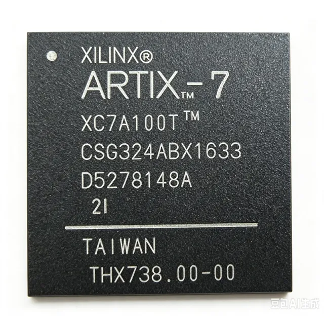
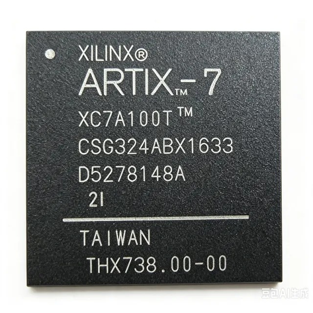
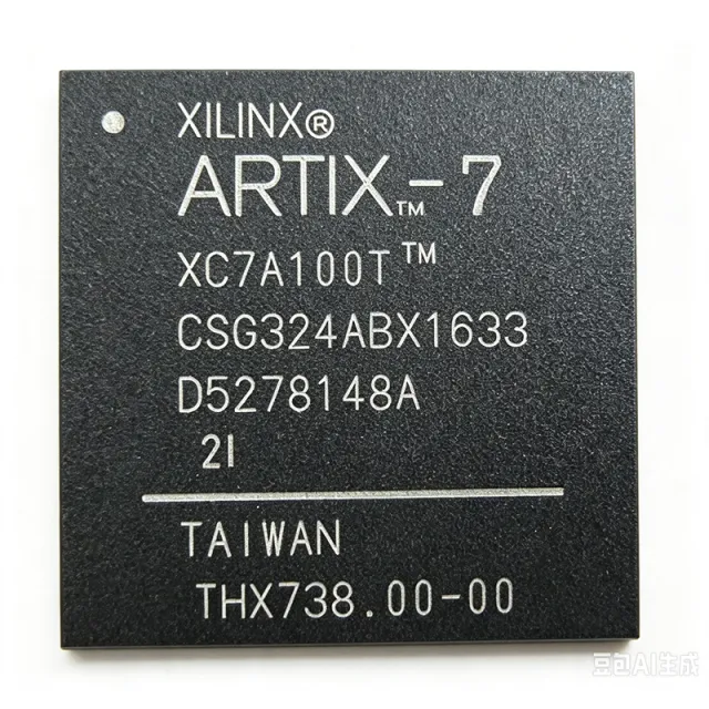
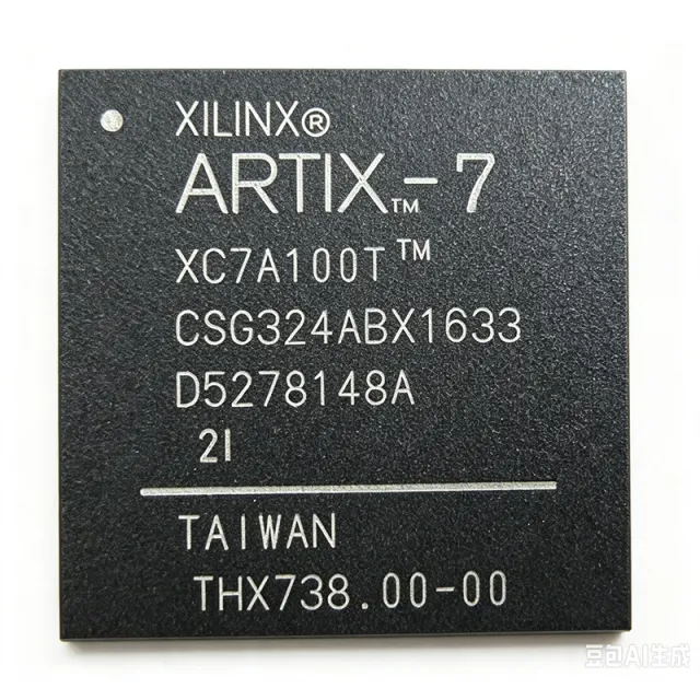
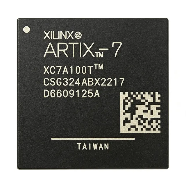
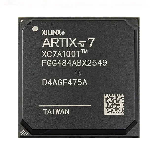
The AMD (Xilinx) XC7A100T is a mid-range member of the Artix-7 family of Field Programmable Gate Arrays (FPGAs) fabricated on TSMC 28nm HPL process, delivering the lowest power and cost per logic cell in the 7-series lineup. The base MPN covers speed grades -1, -2, -3 and commercial/industrial temperature ranges in packages CSG324, FTG256, FGG484, and FGG676. An FPGA (Field Programmable Gate Array) is a semiconductor device containing programmable logic blocks and reconfigurable interconnects that customers configure after manufacturing, enabling custom digital hardware without ASIC development cost. FPGAs sit above CPLDs in capacity and below ASSPs in specificity; the Artix-7 family is positioned as a low-cost, low-power FPGA for high-volume, cost-sensitive systems. Key features of the XC7A100T include 101,440 logic cells (15,850 slices with 6-input LUTs), 4,860 Kb of block RAM, 240 DSP48E1 slices supporting 25x18 multipliers with 48-bit accumulators, 6 clock management tiles (CMTs), and up to 210 user I/O in the CSG324 package. The T suffix denotes transceiver-capable devices supporting serial line rates up to 6.6 Gbps (GTP) in select packages. Integrated hard IP includes PCIe blocks, an XADC 12-bit analog-to-digital converter, and hardened DDR3 memory controller support, reducing external component count. Architecture highlights: CLBs combine two slices with fast carry chains; the block RAM is cascadable as dual-port RAM, ROM, or FIFO; and the DSP48E1 pipeline supports FIR filters and FFTs for software-defined radio and video processing. Mixed-voltage I/O banks support LVCMOS, LVDS, HSTL, and SSTL standards, with 3.3V compatibility for legacy interfaces. Typical applications include software-defined radio, motor control, industrial networking, medical imaging, video and image processing, aerospace and defense prototyping, and education platforms such as the popular Basys/Nexys boards. Its performance-per-watt also suits edge computing and IoT gateways. Design consideration: the device requires multiple rails (VCCINT 1.0V, VCCAUX 1.8V, VCCO per bank) with defined power sequencing and thorough decoupling. Use the AMD Vivado design suite for synthesis and refer to DS181 (Artix-7 DC and AC Switching Characteristics) for timing data. Pricing as of 2026-08-29 from DigiKey and LCSC.

Cotización Contacto
XC7A100T-1CS324I - 101440-Logic-Cell FPGA | AMD
XC7A100T-1CS324I

XC7A100T-1CS324I - 101440-Logic-Cell FPGA | AMD

The AMD XC7A100T-1CS324I is an Artix-7 field-programmable gate array with 101,440 logic cells, 210 I/O, and a 1 V operating voltage, housed in a 324-pin FC-BGA package. The device uses 28 nm FPGA technology and combines programmable logic, block RAM, DSP resources, and programmable I/O in a single surface-mount device. Its -1 speed grade supports designs requiring deterministic performance in industrial-temperature applications. An FPGA is a semiconductor device whose digital logic, memory, and signal-processing blocks are configured after manufacture. An Artix-7 FPGA belongs to the broader programmable-logic hierarchy: FPGA → Artix-7 FPGA → programmable logic device → digital semiconductor. This device provides substantially more configurable logic than small CPLDs while retaining a focused package and I/O structure for embedded control, communications, instrumentation, and embedded processing systems. The verified device listing identifies 101,440 logic cells, 210 I/O, a 1 V supply requirement, 28 nm process technology, and a 324-pin FC-BGA package. The 210 available I/O positions allow external interfaces to be assigned according to the selected device, board, and design constraints. The -1 portion of the ordering code denotes a specific speed grade, while the I suffix identifies the industrial-temperature option. Architecturally, the XC7A100T combines general-purpose programmable logic with dedicated block RAM and digital signal processing resources. This mixed-resource arrangement allows control logic, packet buffering, digital filtering, and data movement to be consolidated in one device instead of being divided among several discrete components. Actual logic utilization, RAM availability, DSP count, and achievable performance depend on the selected Artix-7 device resources and the completed design. Typical applications include industrial automation, industrial Ethernet, instrumentation, embedded control, communications infrastructure, and high-speed signal-processing subsystems. The 324-pin package is appropriate when a design needs more I/O than a smaller FPGA package can offer. It can also support systems requiring a dedicated FPGA for protocol conversion, real-time control, data acquisition, or accelerator logic adjacent to a host processor. The principal design consideration is package and resource validation. Engineers should verify the AMD Artix-7 package pinout and device migration information against the exact ordering code before release, especially when changing speed grade or temperature grade. Power, decoupling, configuration-memory access, clocking, and high-speed I/O layout must also be checked against the manufacturer data sheet and applicable reference designs. This page combines verified device characteristics, package information, price and availability gaps, same-family drop-in candidates, and practical selection guidance. It distinguishes verified facts from unresolved commercial and package-specific data so engineers can assess replacement suitability without treating a different speed grade or temperature grade as an identical substitute.

Cotización Contacto
XC7A100T-1CSG324C - Artix-7 FPGA, 101K Logic Cells | AMD Xilinx
XC7A100T-1CSG324C

XC7A100T-1CSG324C - Artix-7 FPGA, 101K Logic Cells | AMD Xilinx

The AMD Xilinx XC7A100T-1CSG324C is a high-performance Artix-7 family FPGA delivering 101,440 logic cells, 240 DSP slices, and 4,860 Kb of block RAM in a 324-ball CSG (Chip Scale BGA) package. It operates with a core voltage of 1.0V and supports I/O standards up to 3.3V, making it suitable for cost-sensitive, high-volume applications requiring programmable logic. Data verified as of 2026-08-04. An FPGA (Field-Programmable Gate Array) is an integrated circuit that can be configured by the designer after manufacturing, allowing for custom digital logic implementations. FPGAs sit within the broader category of programmable logic devices (PLDs), which are part of the semiconductor industry. They offer a balance between the flexibility of software and the performance of fixed-function ASICs, enabling rapid prototyping and hardware acceleration. Key features include 285,000 system logic cells (equivalent), 240 DSP48E1 slices for digital signal processing, and 4,860 Kb of fast block RAM. The device supports a wide range of I/O standards including LVCMOS, LVDS, and HSTL, with up to 210 user I/O pins in the CSG324 package. The -1 speed grade provides a balance of performance and power, with a maximum clock frequency of approximately 400 MHz for internal logic. The Artix-7 architecture is built on a 28nm high-k metal gate (HKMG) process, offering low static power consumption and high logic density. The device includes integrated PCIe Gen2 blocks, XADC for analog-to-digital conversion, and GTP transceivers (up to 6.6 Gbps) for high-speed serial communication. These features make it a versatile choice for a wide range of applications. Typical applications include software-defined radio, motor control, industrial networking, and video processing. The XC7A100T-1CSG324C is particularly well-suited for applications requiring high I/O count and moderate logic resources, such as interface bridging and protocol conversion. When designing with this FPGA, careful attention must be paid to power supply decoupling and thermal management. The device requires multiple supply rails (VCCINT, VCCAUX, VCCO) and a proper power-up sequence. Use the Xilinx Power Estimator (XPE) to calculate power consumption and design an appropriate thermal solution. This page synthesizes distributor pricing, drop-in alternatives, and practical design notes not found in the AMD Xilinx datasheet, providing a comprehensive resource for engineers evaluating the XC7A100T-1CSG324C.

Cotización Contacto
XC7A100T-1CSG324I - Artix-7 FPGA, 101K Logic Cells | AMD Xilinx
XC7A100T-1CSG324I

XC7A100T-1CSG324I - Artix-7 FPGA, 101K Logic Cells | AMD Xilinx

The AMD Xilinx XC7A100T-1CSG324I is a high-performance Artix-7 family FPGA delivering 101,440 logic cells, 240 DSP48E1 slices, and 4,860 Kb of block RAM in a 324-ball CSBGA package. It operates with a core voltage of 1.0V and supports I/O standards up to 3.3V, making it suitable for cost-sensitive, high-volume applications requiring low power and high throughput. Data verified as of 2026-08-04. An FPGA (Field-Programmable Gate Array) is a semiconductor device containing configurable logic blocks and programmable interconnects that can be programmed after manufacturing to implement any digital logic function. FPGAs sit within the hierarchy of programmable logic devices (PLDs), which are a subset of integrated circuits used for custom digital design without the cost and lead time of ASICs. The Artix-7 family is optimized for low power and cost, balancing performance with affordability for applications like software-defined radio, industrial motor control, and medical imaging. Key features include 285,000 system logic cells equivalent, 240 DSP slices for high-speed signal processing, 4,860 Kb of block RAM, and 6.6 Gb/s GTP transceivers. The device supports DDR3 memory interfaces up to 800 Mb/s and features a 12-bit, 1 MSPS XADC for analog monitoring. The CSG324 package offers 210 user I/O pins, providing flexibility for various board designs. The XC7A100T-1CSG324I is built on 28nm high-k metal gate (HKMG) process technology, balancing performance and power efficiency. It includes hardened memory controllers, PCIe Gen2 blocks, and a security engine for bitstream encryption. The device supports partial reconfiguration, enabling dynamic updates to logic functions without full reconfiguration. Typical applications include software-defined radio (SDR) for its DSP capabilities, industrial motor control for its real-time processing, and medical imaging for its parallel processing throughput. The low power consumption and cost-effectiveness make it ideal for high-volume products. When designing with this FPGA, ensure adequate decoupling capacitors on all power rails and follow the recommended power-up sequence to avoid latch-up. The configuration interface supports multiple modes, including JTAG, SPI, and BPI, allowing flexible system integration. This page synthesizes distributor pricing, drop-in alternatives, and practical design notes not found in the AMD Xilinx datasheet, providing engineers with a comprehensive resource for selection and implementation.

Cotización Contacto
XC7A100T-1CSG324I-Q1 - Artix-7 FPGA, 101K Logic Cells | AMD
XC7A100T-1CSG324I-Q1

XC7A100T-1CSG324I-Q1 - Artix-7 FPGA, 101K Logic Cells | AMD

The AMD XC7A100T-1CSG324I-Q1 is an Artix-7 family FPGA delivering 101,440 logic cells, 240 DSP slices, and 4,860 Kb of block RAM in a 324-ball CSG (Chip Scale) package. It operates with a core voltage of 1.0V and supports up to 210 user I/O pins, making it a versatile choice for cost-sensitive, high-volume applications. An FPGA (Field-Programmable Gate Array) is a semiconductor device containing configurable logic blocks and programmable interconnects, allowing designers to implement custom digital logic after manufacturing. Within the broader hierarchy, an FPGA is a type of programmable logic device (PLD), which falls under the category of integrated circuits (ICs) and ultimately semiconductors. The Artix-7 family specifically targets low-power, high-performance applications, balancing logic density with power efficiency. Key features include 101,440 logic cells, 240 DSP48E1 slices for digital signal processing, and 4,860 Kb of block RAM. The device supports multiple I/O standards including LVCMOS, LVDS, and HSTL, and includes integrated PCIe blocks and GTP transceivers for high-speed serial communication. The -1 speed grade indicates a balanced performance level, while the I temperature grade supports operation from -40°C to +100°C (Tj). The XC7A100T-1CSG324I-Q1 is built on AMD's 28nm process technology, offering a favorable balance of performance, power, and cost. The CSG324 package provides a compact footprint with 324 balls, enabling dense PCB layouts. The device includes configuration support via JTAG, SPI, and BPI interfaces, and features AES bitstream encryption for design security. Typical applications include motor control in industrial automation, software-defined radio (SDR) for communications, medical imaging equipment, and automotive infotainment systems. The -Q1 suffix indicates automotive qualification, making it suitable for automotive applications requiring extended temperature ranges and reliability. When designing with this FPGA, careful attention must be paid to power supply decoupling, with multiple 100nF capacitors placed near each power pin. The configuration interface should be selected based on the system boot requirements, with SPI flash being the most common choice for standalone operation. This page synthesizes distributor pricing, drop-in alternatives, and practical design notes not found in the AMD datasheet, providing engineers with a comprehensive resource for design-in decisions.

Cotización Contacto
XC7A100T-1FG484C - 101440-Cell 28nm FPGA | AMD | 484-BBGA
XC7A100T-1FG484C

XC7A100T-1FG484C - 101440-Cell 28nm FPGA | AMD | 484-BBGA

AMD XC7A100T-1FG484C is a 101,440-cell Artix-7 field-programmable gate array fabricated on a 28 nm CMOS process and supplied in a 484-ball FCBGA package. The device provides 285 I/O, operates from a 1 V core supply, and includes programmable logic, block RAM, DSP resources, MMCM and PLL clock-management capabilities. It is intended for industrial, communications, instrumentation, embedded-processing, and high-performance signal-processing designs requiring substantial programmable logic in a single monolithic device. A field-programmable gate array is a semiconductor whose digital logic and interconnect are configured after manufacture. Within the FPGA product hierarchy, Artix-7 devices combine general-purpose programmable logic with configurable I/O, embedded memory, DSP blocks, and clock-management resources. Compared with a fixed-function ASIC, an FPGA allows design revisions, field updates, and shorter development cycles, while compared with a microcontroller it provides parallel hardware resources and substantially higher signal-processing throughput. The verified device data identifies 101,440 logic cells, 285 I/O, a 1 V supply, a 28 nm process, and a 484-ball FCBGA package. The device also includes MMCM and PLL resources, allowing designers to synthesize, divide, phase-shift, and distribute clocks while supporting multiple clock domains. Its large logic capacity makes it suitable for parallel interfaces, protocol bridges, custom datapaths, embedded control, and test-and-measurement systems. The Artix-7 architecture supports configuration storage, programmable logic, dedicated DSP resources, block RAM, high-speed I/O, and clock management within one device. This integration reduces the number of supporting components in designs requiring parallel data movement or deterministic hardware processing. The 484-ball package also provides a large number of physical connections for high pin-count designs, although exact ball assignments, power requirements, configuration pins, and speed-dependent timing limits must be confirmed against the official AMD package documents before layout. Typical applications include industrial control and automation, industrial Ethernet signal handling, communications infrastructure, test equipment, data acquisition, high-speed interface bridging, and embedded vision processing. In these systems, the FPGA can execute parallel algorithms, implement multiple I/O interfaces, and coordinate clocked processing blocks without relying entirely on sequential processor execution. Its principal trade-off is higher power and design complexity than a small microcontroller or dedicated interface ASIC. PCB design should follow AMD's official Artix-7 package-pinout files and the UG475 package information, including correct ball-grid orientation, power-plane partitioning, decoupling, configuration pins, clock routing, and high-speed I/O constraints. The -1 ordering suffix identifies the performance grade, while the C suffix identifies the commercial temperature option; the exact limits should be verified in the manufacturer ordering guide. This page consolidates verified distributor availability, exact source pricing, family-level drop-in alternatives, package details, and engineering design guidance that can help shorten component evaluation and board bring-up. It also distinguishes verified specifications from parameters that require confirmation from the official AMD documentation.

Cotización Contacto
XC7A100T-1FG484I - 101440-Cell Industrial FPGA | AMD
XC7A100T-1FG484I

XC7A100T-1FG484I - 101440-Cell Industrial FPGA | AMD

The AMD XC7A100T-1FG484I is an Artix-7 field-programmable gate array with 101,440 logic cells, 285 I/O, and a 484-BBGA package. It combines programmable logic, block RAM, digital signal processing resources, and programmable I/O in a single surface-mount device, making it suitable for industrial control, communications, instrumentation, embedded processing, and high-performance embedded systems. The -1 designation identifies the device speed grade, while the I suffix identifies the industrial temperature option. An FPGA is a programmable-logic semiconductor whose digital logic, interconnect, memory, and I/O resources are configured after manufacture. Within the semiconductor hierarchy, an FPGA is a programmable logic device and a complex integrated circuit. Compared with a fixed-function microcontroller or application-specific controller, an Artix-7 FPGA provides parallel processing resources, flexible interfaces, deterministic hardware behavior, and field-updatable configurations. This makes the XC7A100T especially useful when a design requires multiple data paths, high I/O density, or specialized interface timing. The verified product listing identifies 101,440 programmable logic cells, 285 I/O, and a 484-BBGA package. The device is based on 28 nm CMOS FPGA technology and includes programmable logic, block RAM, DSP resources, clock-management circuitry, and high-speed I/O. Its logic-cell and I/O resources support parallel data acquisition, protocol conversion, control-loop implementation, test sequencing, and embedded signal processing. The listed 1.0 V operating reference provides a basis for power planning, although the complete AC and DC limits must be checked in the manufacturer data sheet for every voltage, temperature, and speed condition. The FPGA architecture allows multiple clock domains, registered I/O paths, dedicated memory resources, and parallel processing pipelines. DSP blocks can accelerate fixed-point and filtering operations without relying entirely on a soft processor. Dedicated clock-management and I/O resources support predictable timing when constraints, pin planning, and board-level signal integrity are handled according to the AMD design tools and device documentation. Typical implementations include industrial automation controllers, sensor and instrumentation hubs, communications equipment, data-acquisition systems, embedded vision preprocessing, and custom accelerator modules. The 285 I/O make the device useful for parallel sensor interfaces, digital buses, and control peripherals, while the 101,440 logic cells allow substantial control logic and data pipelines to be implemented on one programmable device. PCB design must account for the 484-ball package, power-supply sequencing, decoupling, ball assignments, high-speed routing, and thermal performance. Designers should use the AMD package pinout files, verify the exact ball map for the ordered MPN, and generate the physical design using the supported Vivado device installation. Configuration storage, clocking, JTAG access, and power rails should be validated before fabrication. This product record combines verified distributor specifications, available Artix-7 alternatives, package-level design guidance, and practical selection considerations. It is intended to support initial sourcing and engineering triage, while production decisions should rely on the current AMD data sheet, package files, design guides, and tool release notes.

Cotización Contacto
XC7A100T-1FGG484I - Artix-7 FPGA, 285 I/O | AMD
XC7A100T-1FGG484I

XC7A100T-1FGG484I - Artix-7 FPGA, 285 I/O | AMD

The AMD XC7A100T-1FGG484I is an Artix-7 Field Programmable Gate Array (FPGA) from the 7 series family, offering a balance of low cost, small form factor, and high performance-per-watt for cost-sensitive, high-volume applications. It features 101,440 logic cells, 285 user I/Os, and 4,976,640 bits of block RAM, all in a 484-pin BGA (FGG484) package. The device operates on a 1V core voltage and is built on 28nm technology, providing a robust platform for a wide range of digital designs. An FPGA (Field Programmable Gate Array) is an integrated circuit that can be configured by the customer or designer after manufacturing. Unlike fixed-function ASICs, FPGAs contain an array of programmable logic blocks and a hierarchy of reconfigurable interconnects that allow the blocks to be wired together in different configurations. This flexibility makes FPGAs ideal for prototyping, low-to-mid volume production, and applications requiring hardware reconfiguration. In the system hierarchy, an FPGA sits above microcontrollers in complexity and parallelism, offering massive parallel processing capabilities for tasks like digital signal processing (DSP), high-speed I/O, and custom logic implementation. Key features of the XC7A100T-1FGG484I include 285 user I/Os, which provide ample connectivity for interfacing with external peripherals and memory. The device also integrates Mixed-Mode Clock Managers (MMCM) and Phase-Locked Loops (PLL) for robust clock generation and management. With 4,976,640 bits of block RAM, it can handle substantial data buffering and storage requirements. The Artix-7 family is optimized for highest performance-per-watt, making it suitable for power-sensitive applications. Technically, the Artix-7 series is built on a 28nm high-k metal gate (HKMG) process, offering a significant improvement in performance and power efficiency over older generations. The device supports various I/O standards, including LVCMOS, LVDS, and HSTL, enabling flexible interfacing. The FGG484 package provides a compact footprint while still offering a high pin count for complex designs. The 'I' suffix indicates an industrial temperature grade, allowing operation from -40°C to +100°C (Tj). Typical applications include software-defined radio, motor control, industrial networking, and video processing. The XC7A100T's combination of logic density, I/O count, and DSP capabilities makes it ideal for these mid-range applications where cost and power are critical. For example, in software-defined radio, the FPGA can handle multiple channels of digital down-conversion and filtering in parallel, offloading the host processor. When designing with this device, careful attention must be paid to power supply decoupling and sequencing. The FPGA requires multiple voltage rails (VCCINT, VCCAUX, VCCO), and proper sequencing is essential to avoid latch-up or damage. Refer to the Xilinx 7 Series FPGAs Power Management Application Note (XAPP) for detailed guidance.

Cotización Contacto
XC7A100T-1FTG256C - Artix-7 FPGA, 101K LCs, 256-FTBGA | AMD
XC7A100T-1FTG256C

XC7A100T-1FTG256C - Artix-7 FPGA, 101K LCs, 256-FTBGA | AMD

The AMD Xilinx XC7A100T-1FTG256C is an Artix-7 family Field Programmable Gate Array (FPGA) housing 101,440 logic cells in a 256-ball FTG (FTBGA-256, 17x17 mm, 1.0 mm pitch) package, with 170 user I/Os, 4,976,640 bits of block RAM, and 240 DSP48E1 slices. The -1 speed grade targets commercial 0°C to 85°C operation and is built on TSMC's 28 nm HPL (high-performance, low-power) HKMG process, balancing logic density with low static and dynamic power. An Artix-7 FPGA is a programmable logic device that occupies the mid-range slot in AMD's 7-series portfolio (Spartan-6 below, Kintex-7 above), optimized for cost-sensitive, high-throughput, power-constrained systems. The 7-series architecture shares a unified ASMBL (Advanced Silicon Modular Block) fabric across all four family members, so Artix-7 inherits 6-input LUTs, 36 Kb block RAM, DSP48E1 slices, and SelectIO with HSTL/DDR memory interfaces from Kintex-7, while trading high-speed serial transceivers for lower die cost. Key features include up to 6.6 Gb/s transceivers on speed-grade /package permutations (the FTG256 omits GTX), integrated PCIe Gen2 hard cores, dual 12-bit 1 Msps ADCs, and clock-management tiles comprising 6 CMTs each with one PLL and one MMCM. A 1.0 V Vccint core, separate Vccaux (1.8 V) and Vcco (1.2-3.3 V HR I/O plus 1.2-1.8 V HP I/O) rails, and an Artix-7-specific power-optimization tier let designers meet thermal envelopes as low as 2-3 W at moderate toggle rates. Typical applications span software-defined radio (SDR) front-ends, machine-vision cameras, industrial motor control and PLCs, low-cost wireless backhaul, avionics flight controllers, and medical imaging pipelines. The FTG256 package balances thermal pad access with 170 single-ended I/Os, so most industrial and instrumentation form factors can be supported without moving to larger FGG484 or FBG676 footprints. When designing with this device, plan decoupling around the FPGA's recommended power-rail decoupling network (one 100 uF bulk per rail plus 0.1 uF + 0.01 uF close to each VRM pin). The FTG256's 1.0 mm ball pitch supports reflow with standard 4-mil NSMD or 5-mil SMD stencils; verify thermal performance with the AMD XPE spreadsheet before committing the PCB. This page synthesizes distributor pricing, package-level drop-in alternatives, and practical Artix-7 design notes - context not duplicated in the official ds181 datasheet.

Cotización Contacto
XC7A100T-2CSG324C - Artix-7 FPGA, 101K Logic Cells | AMD Xilinx
XC7A100T-2CSG324C

XC7A100T-2CSG324C - Artix-7 FPGA, 101K Logic Cells | AMD Xilinx

The AMD Xilinx XC7A100T-2CSG324C is a high-performance Artix-7 family FPGA delivering 101,440 logic cells, 240 DSP48E1 slices, and 4,860 Kb of block RAM in a 324-ball CSBGA (CSG324) package. It operates with a core voltage of 1.0V and supports I/O standards including LVCMOS, LVDS, and HSTL across 210 user I/O pins. Data verified as of 2026-08-04. An FPGA (Field-Programmable Gate Array) is a semiconductor device containing configurable logic blocks (CLBs), programmable interconnects, and I/O blocks that can be programmed after manufacturing to implement custom digital logic circuits. FPGAs sit within the broader category of programmable logic devices (PLDs), which are part of the application-specific integrated circuit (ASIC) family, but unlike ASICs, FPGAs offer reconfigurability, making them ideal for prototyping, low-volume production, and applications requiring in-field updates. Key features of the XC7A100T-2CSG324C include 101,440 logic cells, 240 DSP slices for high-speed signal processing, 4,860 Kb of block RAM, and 6 CMTs (Clock Management Tiles) providing PLL and MMCM for robust clock generation. The device supports PCIe Gen2 x1, Gigabit Ethernet, and DDR3 memory interfaces, making it suitable for a wide range of embedded and communications applications. The -2 speed grade offers a balance of performance and power, with a maximum clock frequency of 400 MHz for block RAM and 600 MHz for I/O. The Artix-7 architecture is built on a 28nm high-k metal gate (HKMG) process, delivering low static power consumption and high logic density. The device includes hardened memory controllers for DDR3, and its SelectIO technology supports up to 1.25 Gbps LVDS, enabling high-speed data transfer. The CSG324 package measures 15x15 mm with a 0.8 mm ball pitch, providing a compact footprint for space-constrained designs. Typical applications include software-defined radio (SDR), motor control, industrial Ethernet, medical imaging, and video processing. The XC7A100T-2CSG324C is particularly suited for applications requiring high DSP throughput and moderate logic capacity, such as digital signal processing in radar and communication systems. When designing with this FPGA, careful attention must be paid to power supply decoupling, with multiple 100nF capacitors placed near each power pin, and to thermal management, as the device can dissipate up to 2.5W under full utilization. The configuration bitstream can be stored in SPI flash, and the device supports multi-boot for remote updates. This page synthesizes distributor pricing, drop-in alternatives, and practical design notes not found in the AMD Xilinx datasheet, providing engineers with a comprehensive resource for selecting and implementing the XC7A100T-2CSG324C.

Cotización Contacto
XC7A100T-2CSG324I - Artix-7 FPGA, 101K Logic Cells | AMD Xilinx
XC7A100T-2CSG324I

XC7A100T-2CSG324I - Artix-7 FPGA, 101K Logic Cells | AMD Xilinx

The AMD Xilinx XC7A100T-2CSG324I is a high-performance Artix-7 family FPGA delivering 101,440 logic cells, 240 DSP slices, and 4,860 Kb of block RAM in a 324-ball CSG (Chip-Scale BGA) package. It operates over the industrial temperature range (-40°C to +100°C) and is designed for cost-sensitive, high-volume applications requiring low power and high throughput. An FPGA (Field-Programmable Gate Array) is a semiconductor device containing a matrix of configurable logic blocks (CLBs) connected by programmable interconnects, allowing designers to implement custom digital logic circuits after manufacturing. FPGAs sit within the broader category of programmable logic devices (PLDs), which are part of the larger family of integrated circuits (ICs). Unlike fixed-function ASICs, FPGAs offer reconfigurability, enabling rapid prototyping and field upgrades, making them essential in applications ranging from embedded vision to software-defined radio. Key features of the XC7A100T-2CSG324I include 285,120 flip-flops, 240 DSP48E1 slices (each capable of 25x18 multiplication), and 135 Block RAM blocks (36 Kb each) totaling 4,860 Kb. The device supports up to 300 user I/O pins with support for multiple I/O standards including LVCMOS, LVDS, and HSTL. It integrates a 12-bit, 1 MSPS XADC for analog monitoring and supports PCIe Gen2 x1 and 10/100/1000 Ethernet via hardened blocks. The -2 speed grade provides balanced performance, with internal clock speeds up to 628 MHz. The Artix-7 architecture is built on a 28 nm high-k metal gate (HKMG) process, offering a 50% lower static power compared to previous generations. The device includes a unified configuration interface supporting JTAG, SelectMAP, and Quad-SPI flash programming. Its low-power transceivers (up to 16 GTP transceivers at 6.6 Gbps) enable high-speed serial connectivity for applications like video over SDI and CPRI. Typical applications include software-defined radio (SDR), medical imaging, motor control, and industrial Ethernet. The XC7A100T-2CSG324I is particularly suited for designs requiring high logic density with moderate I/O counts, such as camera-based vision systems and test equipment. Its industrial temperature grade makes it reliable for harsh environments. For detailed specifications, refer to the official AMD Xilinx datasheet (DS181) and the Artix-7 FPGA product page at https://www.xilinx.com/products/silicon-devices/fpga/artix-7.html. When designing with this FPGA, careful attention must be paid to power supply decoupling and PCB layout to ensure signal integrity at high speeds. The device requires multiple supply rails (VCCINT, VCCAUX, VCCO) with specific sequencing, and the use of the XADC for thermal monitoring is recommended to prevent overheating.

Cotización Contacto
XC7A100T-2FBG484I - Artix-7 FPGA, 101K Logic Cells | AMD
XC7A100T-2FBG484I

XC7A100T-2FBG484I - Artix-7 FPGA, 101K Logic Cells | AMD

The AMD XC7A100T-2FBG484I is a high-performance Artix-7 Field Programmable Gate Array (FPGA) from the 7 Series family, offering 101,440 logic cells, 285 user I/Os, and 4,976,640 bits of block RAM in a 484-ball FBGA package. It operates over an industrial temperature range of -40°C to +100°C and is designed for cost-sensitive applications requiring high performance-per-watt. An FPGA (Field Programmable Gate Array) is an integrated circuit that can be configured by the customer after manufacturing to implement arbitrary digital logic functions. FPGAs sit between ASICs (application-specific ICs) and microprocessors in the design hierarchy: they offer the parallelism and determinism of custom hardware with the reconfigurability of software. The Artix-7 family is optimized for the lowest power and cost at 28nm, making it a popular choice for embedded vision, software-defined radio, and industrial automation. Key features of the XC7A100T-2FBG484I include 285 user I/Os, 4,976,640 bits of block RAM, 240 DSP slices, and support for MMCM and PLL clock management. The -2 speed grade provides a maximum clock frequency of 628 MHz, while the industrial temperature rating ensures reliable operation in harsh environments. The device supports VCCINT from 0.95V to 1.05V, enabling flexible power supply design. Architecturally, the Artix-7 fabric is built on a 28nm high-k metal gate (HKMG) process, delivering a 50% reduction in power consumption compared to previous generations. The device integrates AMS (Analog Mixed Signal) blocks, including a 12-bit 1 MSPS ADC, for on-chip monitoring of voltage and temperature. This integration reduces external component count and simplifies board design. Typical applications include software-defined radio, motor control, industrial Ethernet, and medical imaging. The 484-ball FBGA package provides a balanced pin count for medium-complexity designs, while the industrial temperature range makes it suitable for outdoor and automotive-adjacent deployments. When designing with this device, ensure adequate decoupling on all power rails (VCCINT, VCCAUX, VCCO) and follow AMD's power-on sequencing guidelines to avoid latch-up. The configuration bitstream can be stored in external SPI flash or loaded via JTAG, with support for multi-boot for remote updates.

Cotización Contacto
XC7A100T-2FG484C - 101440-Cell Artix-7 FPGA | AMD
XC7A100T-2FG484C

XC7A100T-2FG484C - 101440-Cell Artix-7 FPGA | AMD

The AMD XC7A100T-2FG484C is a 101,440-cell Artix-7 field-programmable gate array built on 28 nm CMOS technology, with 285 I/O, a 1 V core configuration supply, and a 484-ball BGA package. The device belongs to the FPGA and CPLD hierarchy, where programmable logic fabric, block RAM, DSP resources, and configurable I/O are integrated on one semiconductor package. An FPGA is a reconfigurable digital integrated circuit used to implement control logic, signal processing, interface conversion, protocol handling, and data acquisition functions without changing the physical circuit board. Unlike a fixed-function application-specific integrated circuit, an Artix-7 FPGA can be reprogrammed during development or field updates to alter logic, add functions, or support design revisions. This makes the XC7A100T useful when algorithms and system interfaces evolve rapidly. The Artix-7 family balances programmable logic capacity with power efficiency and cost. The XC7A100T provides 101,440 logic cells and 285 I/O, making it suitable for industrial controllers, embedded vision systems, communications equipment, instrumentation, and high-bandwidth signal-processing platforms. The -2 ordering designation identifies the specified performance grade, while the 484-ball package provides a substantial connection count for external memory and peripheral interfaces. Exact clock, memory, DSP, I/O-standard, and temperature details require confirmation in the manufacturer datasheet. The device is appropriate for designs that require substantial programmable logic but do not need the resources of a larger FPGA family. It can implement parallel data paths, state machines, sensor fusion, industrial protocols, control loops, and test logic while keeping the design flexible. Its 28 nm process technology also places it within AMD's cost-sensitive, power-efficient Artix-7 positioning. A valid package drawing, pinout data, power plan, configuration method, and board-level design must be treated as one system. Before schematic capture and PCB layout, engineers should obtain the exact AMD package pinout files, verify the accepted supply rails, and confirm which I/O standards and configuration pins are available for the selected board revision. For a drop-in sourcing decision, package and pinout compatibility alone is insufficient. The replacement must also provide equivalent logic resources, memory interfaces, configuration behavior, speed grade, temperature grade, and power characteristics. This page distinguishes verified distributor information from parameters that still require confirmation from the official Artix-7 documentation. This page combines the supplied distributor data, Artix-7 package references, and structured comparison information to support engineering selection. It also identifies uncertain fields explicitly instead of presenting unverified values as guaranteed specifications.

Cotización Contacto
XC7A100T-2FGG484I - Artix-7 FPGA, 285 I/O, 484-FBGA | AMD
XC7A100T-2FGG484I

XC7A100T-2FGG484I - Artix-7 FPGA, 285 I/O, 484-FBGA | AMD

The AMD XC7A100T-2FGG484I is an Artix-7 Field Programmable Gate Array (FPGA) featuring 101,440 logic cells, 285 user I/Os, and 4,976,640 bits of block RAM, fabricated on a 28nm process and housed in a 484-ball Fine-Pitch Ball Grid Array (FBGA/FGG484) package rated for the industrial temperature range of -40C to +100C. An FPGA is a reconfigurable integrated circuit whose logic fabric, interconnect, and I/O cells can be programmed after manufacturing, unlike fixed-function ASICs. Within the hierarchy of programmable logic, the Artix-7 family sits between the smaller Spartan-7 and the larger Kintex-7 in AMD's (formerly Xilinx) 7-series, balancing logic density, DSP throughput, and transceiver performance for cost-optimized mid-range designs. Key differentiating features include 240 DSP48E1 slices for parallel signal processing, 10 clock management tiles (CMTs) combining MMCM and PLL blocks, and support for MicroBlaze soft processor cores and DDR3 memory interfaces up to 1,066 Mb/s. The -2 speed grade fabric can run at up to 628 MHz, and the device integrates Analog Mixed Signal (AMS) blocks including a 12-bit ADC for on-chip voltage and temperature monitoring. Architecturally, the 28nm high-performance/low-power process enables high logic utilization with low static power. The core supply operates from 0.95V to 1.05V nominal 1.0V, with separate VCCAUX and bank-selectable VCCO rails supporting multiple I/O voltage standards. Partial reconfiguration allows flexible in-system updates without full device reprogramming. Typical applications include motor control, industrial networking and automation, medical imaging front ends, and software-defined radio, where the 285 I/O count and DSP density are well matched. The 484-ball FGG484 package offers a balanced footprint of approximately 23mm x 23mm for moderate-to-high I/O designs. A key design consideration is power: multiple rails (VCCINT, VCCAUX, VCCO) require specific power sequencing, ramp rates, and decoupling networks. Use the AMD Vivado Design Suite for implementation and the UG475 package pinout files for PCB footprint verification. This page synthesizes distributor pricing, drop-in alternatives, and practical design notes not found in the manufacturer datasheet, as of 2026-09-11.

Cotización Contacto
XC7A100T-2FT256I - 170 I/O Artix-7 FPGA | AMD
XC7A100T-2FT256I

XC7A100T-2FT256I - 170 I/O Artix-7 FPGA | AMD

The AMD Xilinx XC7A100T-2FT256I is a 170 I/O Artix-7 field-programmable gate array supplied in a 256-ball FTBGA package. It combines programmable logic, fixed-point DSP resources, block RAM, and programmable I/O in a single low-power device for industrial embedded, control, signal-processing, and communications systems. The -2 ordering code identifies the -2 performance grade, while the I suffix identifies the industrial temperature option. An FPGA is a programmable semiconductor whose digital logic blocks, interconnections, and peripheral resources are configured after manufacture. Within the semiconductor hierarchy, the Artix-7 device belongs to the FPGA and CPLD family of programmable logic devices. Compared with a fixed-function ASIC, an FPGA allows design changes, parallel processing, and hardware acceleration without redesigning an integrated circuit. The XC7A100T-2FT256I provides 170 user I/O in the verified distributor records, with the 256-FTBGA package providing the physical interconnect for those interfaces. The -2 speed grade is the central performance designation for this ordering code. Its Artix-7 architecture supports parallel datapath and control implementations where deterministic, configurable hardware is more useful than a sequential processor-only approach. Typical uses include industrial automation, embedded instrumentation, test and measurement, embedded video, communications gateways, and digital signal-processing front ends. Parallel ADC data can be captured, filtered, transformed, and routed without transferring every sample through a general-purpose processor. The large logic fabric also allows protocol bridging, real-time data reduction, and hardware-assisted control to be consolidated into one programmable device. Board design requires careful decoupling, multilayer construction, controlled clock routing, and complete BGA fanout. Because the package contains solder-ball connections rather than exposed leads, inspection and assembly require X-ray or equivalent process verification. The device should be paired with a correctly specified configuration memory and a validated clocking and power-delivery network. This page consolidates distributor availability information, Artix-7 package details, speed-grade alternatives, application guidance, and design cautions that are distributed across individual distributor and datasheet listings. Engineering decisions should still be checked against the current AMD Artix-7 data sheet, package files, and the specific configuration memory interface.

Cotización Contacto
XC7A12T-1CPG238C - 12,800-LC Artix-7 FPGA | AMD
XC7A12T-1CPG238C

XC7A12T-1CPG238C - 12,800-LC Artix-7 FPGA | AMD

The AMD XC7A12T-1CPG238C is an Artix-7 field-programmable gate array with 12,800 logic cells, 40 DSP slices, 720 Kbit of block RAM, and 106 I/O, supplied in a 238-ball CSBGA package. It combines programmable logic, fixed DSP resources, block memory, and general-purpose I/O in a compact surface-mount device intended for cost-sensitive, low-power embedded systems. An FPGA is a semiconductor whose digital functionality is defined after fabrication through a configuration bitstream. Within the product hierarchy, this Artix-7 device belongs to the Xilinx 7 Series FPGA family and combines a configurable logic array with programmable I/O blocks, DSP slices, block RAM, and dedicated configuration resources. This makes it more flexible than a fixed-function application-specific integrated circuit while providing more integration than a collection of discrete logic devices. The verified specifications identify 12,800 logic cells, 737,280 bits of block RAM, 40 DSP slices, and 106 I/O. The AMD Artix-7 product page states that the family uses a 28 nm process and is optimized for low-power applications requiring serial transceivers and high DSP and logic throughput. These attributes make the device suitable for embedded control, industrial automation, communications, and signal-processing systems where firmware updates and reconfigurable hardware add practical value. The XC7A12T designation identifies the Artix-7 device family and its resource level, while the -1 designation identifies the performance grade. The CPG238 suffix identifies the compact 238-ball package used by the device. Distributor listings also describe the package as 238-LFBGA or CSPBGA. Because the exact target MPN uses the commercial-temperature suffix C, engineers should confirm the complete ordering information, pinout, configuration requirements, and operating-temperature requirements against the AMD package and product documentation before releasing a design. Typical uses include industrial control and factory automation, low-power embedded processing, communications equipment, sensor aggregation, and compact DSP-based products. The 40 DSP slices support parallel arithmetic operations, while 720 Kbit of block RAM allows data buffering and local storage without relying entirely on external memory. The 106 I/O count supports interfaces to sensors, transceivers, converters, and discrete digital peripherals when the selected I/O standards and voltage banks permit them. A practical design priority is to complete pin planning before layout. AMD provides Artix-7 package pinout files in TXT and CSV formats, and those files should be used to confirm every ball assignment, configuration pin, supply pin, and exposed-pad connection. Designers must also verify that the PCB stack-up, via pattern, power distribution, and decoupling arrangement meet the package and platform requirements. This product record combines distributor availability, package details, Artix-7 family characteristics, and a same-family replacement analysis. It also distinguishes verified device facts from unavailable electrical details, avoiding unsupported assumptions about voltage ratings, temperature limits, pin functions, and lifecycle commitments.

Cotización Contacto
XC7A12T-1CSG325I - 12,800-Cell Artix-7 FPGA | AMD
XC7A12T-1CSG325I

XC7A12T-1CSG325I - 12,800-Cell Artix-7 FPGA | AMD

The AMD XC7A12T-1CSG325I is an Artix-7 field-programmable gate array with 12,800 logic cells, 150 I/O, and 28 nm fabrication technology in a 325-pin CSBGA package. The verified distributor data also identifies 737,280 as an associated device figure and lists a 1 V core supply value. These figures position the device as a compact FPGA platform for embedded control, industrial automation, communications, instrumentation, and cost-sensitive designs that require programmable logic and a substantial pin count. A field-programmable gate array is a semiconductor whose digital logic, memory, and I/O behavior can be configured after manufacture. Within the product hierarchy, an FPGA is a programmable-logic device and a semiconductor. The Artix-7 family combines programmable logic resources with a relatively compact package, allowing engineers to consolidate functions that might otherwise require separate processors, glue logic, and interface devices. The XC7A12T-1CSG325I specifically uses a CSBGA package with 324-LFBGA/CSPBGA notation in the verified distributor listings. The principal verified attributes are the 12,800-cell Artix-7 logic capacity, 150 available I/O, 28 nm process technology, 1 V value, and 325-pin package. The 150-I/O count is particularly useful for parallel data acquisition, multiple external memory interfaces, control signals, and high-pin-count communication peripherals. The large BGA land pattern also supports dense routing in multilayer PCB designs, but it requires careful escape routing, via planning, and assembly-process control. This is an FPGA rather than a fixed-function microcontroller, so the implemented design is defined by the bitstream loaded into the device. That architecture allows logic behavior to be revised without changing the PCB when requirements evolve. It also makes configuration memory, startup sequencing, clocking, decoupling, and I/O standards central engineering considerations. Exact block counts, memory resources, supported interfaces, performance grades, power limits, and electrical characteristics beyond the supplied verified values require the AMD device documentation before design release. Typical uses include industrial factory automation, industrial motor and motion control, network-interface equipment, test and measurement systems, embedded instrumentation, and compact communications platforms. In these applications, the 150 I/O and 12,800 logic cells can consolidate parallel control, acquisition, protocol, and data-processing functions, while the Artix-7 device family provides a path to hardware specialization and field updates. PCB planning should prioritize the BGA escape path, layer transitions, clean power distribution, and thermal spreading around the device. Because the verified package is not represented by an available canonical SVG package key, the pinout is not reproduced here. Engineers should use the official AMD Artix-7 package pinout files to verify every ball assignment, power pin, configuration pin, and keep-out region before layout release. This page consolidates verified distributor specifications, package information, sourcing links, comparison fields, and engineering cautions for XC7A12T-1CSG325I. It separates documented values from unavailable technical data and avoids presenting unverified performance, pricing, pin assignments, compliance claims, or replacement parts as established facts.

Cotización Contacto
XC7A12T-2CPG238C - 12.8K Artix-7 FPGA | AMD
XC7A12T-2CPG238C

XC7A12T-2CPG238C - 12.8K Artix-7 FPGA | AMD

The AMD XC7A12T-2CPG238C is an Artix-7 field-programmable gate array with 12,800 logic cells, 106 user I/Os, and a 1.0 V core in a 238-pin CSPBGA package. Designed for cost-sensitive, power-conscious programmable-logic applications, the device uses 28 nm HKMG technology and is available in a compact 10 mm × 10 mm package. Its -2 speed designation identifies the performance grade, while the C suffix denotes the commercial temperature option. An FPGA is a programmable semiconductor in the broader semiconductor and digital-logic hierarchy. Unlike a fixed-function application-specific integrated circuit, an FPGA combines configurable logic blocks, programmable interconnect, block RAM, digital signal processing resources, and general-purpose I/O in one device. Artix-7 belongs to the FPGA family within programmable-logic devices and combines moderate logic capacity with low power consumption for cost-sensitive embedded designs. The XC7A12T provides 12,800 logic cells and 106 user I/Os, making it suitable for parallel data acquisition, control logic, communications bridges, industrial interfaces, and embedded signal-processing systems. The 238-pin CSPBGA package offers substantially more external connections than a leaded FPGA package, supporting high-pin-count interfaces while keeping the device physically compact. The 1.0 V core supply is an important integration constraint for systems using modern low-voltage FPGA logic. The device is fabricated on 28 nm HKMG technology. This process places the XC7A12T between higher-capacity programmable devices and simpler fixed-function controllers in cost and integration terms. Its 106 I/Os allow designers to connect external memory, converters, transceivers, clocks, and parallel data sources directly to configurable logic. The supplied distributor data identifies the Artix-7 architecture but does not expose detailed block RAM, DSP slice, maximum clock, or I/O performance figures. Typical applications include industrial control and automation, communications and networking interfaces, instrumentation, embedded vision, sensor aggregation, and low-power portable equipment. In these systems, the FPGA can consolidate parallel interfaces, protocol conversion, timing, data acquisition, and control functions while shortening development time compared with multiple fixed-function devices. The 10 mm × 10 mm CSPBGA also supports space-constrained board layouts when careful escape routing and multilayer PCB construction are used. The principal design consideration is BGA implementation. A 238-ball package requires a multilayer PCB, controlled via geometry, adequate solder-mask and paste design, X-ray inspection, and a temperature-controlled assembly profile. Designers must also verify the complete power tree for the 1.0 V core and associated I/O supply requirements rather than assuming that one rail satisfies the device. This page combines verified distributor specifications with practical selection guidance, package considerations, and engineering-focused comparisons. It separates known values from unavailable details so procurement teams can identify supply, fit, and lifecycle risks before committing the XC7A12T-2CPG238C to an FPGA-based design.

Cotización Contacto
XC7A12T-2CSG325I - 12.8K Logic Cell Artix-7 FPGA | AMD
XC7A12T-2CSG325I

XC7A12T-2CSG325I - 12.8K Logic Cell Artix-7 FPGA | AMD

AMD XC7A12T-2CSG325I is an Artix-7 field-programmable gate array with 12,800 logic cells, 150 user I/Os, 737,280 internal configuration memory bits, and a -2 performance grade in a 324-LFBGA CSBGA package. Built on 28 nm HKMG HPL process technology, this FPGA targets cost-sensitive, low-power designs requiring moderate logic density and serial connectivity. An FPGA is a reconfigurable digital semiconductor whose programmable logic, memory blocks, and programmable I/O can be configured after manufacture. The Artix-7 family combines a low-cost FPGA architecture with resources suited to embedded processing, control logic, communication interfaces, and general-purpose digital systems. XC7A12T-2CSG325I is the smallest logic-density member of this Artix-7 family as identified by the verified 12,800-logic-cell specification. The device provides 150 user I/Os, allowing a compact design to expose substantial external connectivity despite its relatively small logic capacity. Its 737,280 configuration-memory bits provide the nonvolatile storage used to define the implemented logic and interconnect configuration. The -2 speed designation identifies its performance grade, while the CSBGA package supports compact, high-density PCB integration. The 28 nm HKMG HPL process provides the physical foundation for the device's low-power, cost-sensitive positioning. Available design resources can be assigned for control, data acquisition, interface bridging, embedded signal processing, or general programmable logic. Exact block counts, memory capacity, supported I/O standards, operating-temperature limits, and recommended operating conditions are not present in the supplied source excerpts and therefore should not be inferred. Typical applications include industrial control modules, low-power embedded systems, communication interfaces, video and image-processing front ends, instrumentation, and consumer or embedded products that benefit from reconfigurable logic. The 150 I/Os are especially useful when an external processor, memory, transceiver, or mixed-signal interface requires multiple parallel connections. PCB planning should use the official AMD Artix-7 package pinout files rather than generic BGA assumptions. Decoupling, power sequencing, configuration-interface routing, and thermal management must follow the applicable AMD seven-series guidance, and unused balls should not be assigned functions without consulting the package data. This page consolidates verified distributor specifications, package information, availability, and design guidance into one engineering-focused reference. It also distinguishes the only verified same-package alternatives from different-package devices that may be functionally similar but cannot replace the target without PCB and design changes.

Cotización Contacto
XC7A15T-1CPG236C - 16,640 Logic Cell Artix-7 FPGA | AMD
XC7A15T-1CPG236C

XC7A15T-1CPG236C - 16,640 Logic Cell Artix-7 FPGA | AMD

AMD XC7A15T-1CPG236C is an Artix-7 field-programmable gate array with 16,640 logic cells, 106 I/Os, 921,600 bits of block RAM, and up to 464 DSP slices in a 238-ball CSPBGA package. It combines programmable logic, fixed DSP resources, block RAM, and high-speed I/O in a compact device intended for cost-sensitive, power-efficient embedded processing. An FPGA is a reconfigurable semiconductor in the programmable-logic hierarchy: FPGA > programmable logic device > digital semiconductor. Unlike a fixed-function microcontroller or DSP, an FPGA allows parallel circuits, interfaces, and signal-processing pipelines to be defined in programmable hardware. The Artix-7 family combines this flexibility with a 28 nm process and an optimized balance of performance per watt, logic density, DSP capability, and cost. The XC7A15T-1CPG236C provides 16,640 logic cells for control logic, state machines, protocol handling, and parallel datapaths. Its 921,600 bits of block RAM support buffering, packet storage, and data-domain conversion, while 464 DSP slices accelerate filters and other multiply-accumulate operations. The -1 speed designation identifies the device's performance grade, and the C commercial-temperature designation supports designs in commercial temperature conditions. The 238-CSBGA package exposes 106 user I/Os according to distributor records. This combination makes the device useful where a relatively compact programmable device is needed with both dedicated DSP resources and general-purpose logic. Exact package dimensions, voltage ratings, differential-I/O standards, and supported transceiver capabilities were not supplied in the verified records and should be confirmed in the AMD family documentation before schematic release. Typical uses include software-defined radio front ends, industrial automation, machine-vision image processing, embedded control, communication infrastructure, and digital signal processing. Parallel FIR filters, interpolation, decimation, modulation stages, and sensor-data pipelines can be mapped to the DSP slices while control and interface logic occupy the programmable fabric and block RAM. PCB implementation requires careful assignment of the 238-ball BGA footprint, multilayer escape routing, and verified power, ground, and I/O standards. The design should also include bitstream-generation, timing-analysis, and JTAG programming steps using the corresponding Artix-7 device support. This page combines verified distributor data with engineering-oriented guidance, comparison points, and clearly identified data gaps for design review.

Cotización Contacto
XC7A15T-1CSG324C - 16.6K Logic Cell Artix-7 FPGA | AMD
XC7A15T-1CSG324C

XC7A15T-1CSG324C - 16.6K Logic Cell Artix-7 FPGA | AMD

AMD XC7A15T-1CSG324C is an Artix-7 field-programmable gate array built on a 28 nm process, with 16,640 logic cells, 210 I/Os, and a 324-ball chip-scale BGA package measuring 15 mm by 15 mm. The device operates from 0.95 V to 1.05 V and is rated for a nominal 1.464 GHz maximum data rate, while the -1 speed designation corresponds to a maximum operating frequency of 464 MHz in the supplied device data. An FPGA is a reconfigurable digital semiconductor containing programmable logic blocks, block RAM, digital signal processing resources, and programmable I/O. Artix-7 FPGAs occupy the low-power and cost-sensitive level of the AMD FPGA hierarchy, combining programmable hardware with serial transceiver, DSP, and general-purpose logic throughput. The XC7A15T therefore serves as a compact hardware platform for parallel data acquisition, protocol conversion, control, and embedded signal-processing functions. The XC7A15T-1CSG324C provides 1,300 configurable logic blocks, 900 KB of block RAM, 210 I/Os, and integrated DSP resources. Its nominal 1 V core supply allows implementation on a 0.95 V to 1.05 V power rail. MMCM and PLL resources support clock generation and management, while the high I/O count permits interfaces to external memory, converters, network transceivers, and industrial peripherals. The device combines configurable logic with dedicated hard resources for high-throughput digital processing. Block RAM can buffer sampled data or store lookup tables, while DSP slices accelerate multiply-and-accumulate operations commonly required by filtering and waveform transformations. The -1 performance designation establishes the device's timing class; implementation timing must still be checked against the selected AMD toolchain, pin constraints, clocking plan, and system-level I/O timing requirements. Typical uses include industrial automation, machine-vision image processing, communications protocol bridging, low-cost test equipment, and embedded real-time signal processing. Its 210-I/O footprint is especially useful when a design requires numerous parallel connections while retaining programmable logic and DSP capability in one device. Board design should follow the AMD Artix-7 package pinout files and UG475 guidance, particularly for power, ground, configuration, clock, and high-speed I/O connections. Decoupling, signal-integrity checks, thermal planning, configuration-interface design, and bank-specific voltage constraints should be completed before layout release. This page combines manufacturer and distributor data with the supplied cross-reference results to summarize device identity, procurement considerations, verified alternatives, and practical FPGA design guidance. The listed LCSC price is a product-page reference rather than a guaranteed quotation, so availability and volume pricing should be reconfirmed before purchase.

Cotización Contacto
XC7A15T-1CSG324I - 16,640-LC Artix-7 FPGA | AMD
XC7A15T-1CSG324I

XC7A15T-1CSG324I - 16,640-LC Artix-7 FPGA | AMD

AMD XC7A15T-1CSG324I is an Artix-7 field-programmable gate array with 16,640 logic cells, 210 I/Os and 45 DSP slices in a 324-CSPBGA package. It uses 28 nm fabrication technology, operates from a 1 V core supply and is specified for the industrial temperature range of -40 °C to +100 °C junction temperature. The device is a cost-sensitive FPGA platform intended for compact, high-volume embedded systems requiring programmable logic, DSP and parallel I/O. An FPGA is a semiconductor whose digital logic, interconnect and signal-processing resources are configured after manufacture. Within the product hierarchy, an FPGA is a programmable-logic semiconductor and a reconfigurable digital IC. The XC7A15T belongs to AMD's Artix-7 family, combining general-purpose programmable logic with block RAM, DSP48 processing and high-performance I/O in a relatively small package. The verified specifications identify 16,640 logic cells, 210 I/Os, 921,600 internal configuration bits and 45 DSP slices. Its 324-CSPBGA package is identified in distributor records as a 324-LFBGA/CSPBGA, while an independent market listing specifies a 15 mm × 15 mm body. The -1 suffix denotes the device speed grade, the CSG324 suffix identifies the package, and the I suffix identifies industrial-temperature production. The Artix-7 architecture supports parallel processing, programmable I/O and dedicated DSP resources rather than implementing the complete design in fixed-function logic. This allows the same board design to be reused across multiple product variants through bitstream changes. The 45 DSP slices are especially relevant to filtering, fixed-point arithmetic, signal conditioning and control-loop workloads, while 210 I/Os support parallel buses, sensor acquisition and external memory interfaces. Typical applications include industrial automation, test and measurement, embedded control, communications, camera and image-processing interfaces, and compact instrumentation. The device is appropriate when deterministic parallel I/O and field-updatable logic are more valuable than the very high performance or very high logic density available from larger FPGA families. A complete design still requires suitable memory, clocking, power rails and high-speed PCB layout. Designers should use the AMD package pinout files and UG475 package guidance to map every CSG324 ball. Power, decoupling, configuration access, clocking and high-speed routing must follow the manufacturer's Artix-7 guidance. The industrial temperature rating applies to junction temperature and must be considered together with actual enclosure temperature, board heating and the device's power dissipation. This page consolidates verified distributor specifications, package details, temperature and speed-grade information into an engineering-focused selection reference. It also distinguishes documented drop-in options from unverified equivalents, provides comparison parameters, and identifies the application constraints that require datasheet and board-level review before procurement.

Cotización Contacto
XC7A15T-1FTG256C - 16,640-Cell Artix-7 FPGA | AMD
XC7A15T-1FTG256C

XC7A15T-1FTG256C - 16,640-Cell Artix-7 FPGA | AMD

The AMD XC7A15T-1FTG256C is an Artix-7 field-programmable gate array with 16,640 logic cells, 170 I/Os, and operation up to 464 MHz in a 256-ball FTBGA package. Designed for cost-sensitive, power-efficient embedded systems, this device combines programmable logic, DSP processing, block RAM, MMCM, PLL, and analog mixed-signal resources in a single 28 nm FPGA. An FPGA is a semiconductor whose digital logic, interconnect, and dedicated processing blocks are configured through a bitstream after fabrication. The Artix-7 family belongs to the broader programmable-logic hierarchy: FPGA, programmable logic device, digital semiconductor, and integrated circuit. This balance of logic density, I/O availability, and processing capability makes the XC7A15T suitable for embedded control, communications, industrial automation, machine vision, and prototype hardware. Key features include 16,640 programmable logic cells, 170 user I/Os, a maximum clock rating of 464 MHz, and a 950 mV to 1.05 V core-voltage range identified in the verified sources. The device also includes MMCM and PLL resources according to the product listing, along with DSP and analog mixed-signal capabilities described for the Artix-7 family. The -1 suffix identifies the device speed grade, while the C suffix denotes the commercial temperature option. The 256-ball FTBGA package supports dense board integration without relying on a large leaded footprint. Because a complete, verified ball-by-ball pin list was not included in the supplied source set, engineers should use AMD's official Artix-7 package pinout files before assigning signals, power planes, or configuration pins. Device configuration, I/O standards, and board-level connectivity must follow those package-specific files rather than general device assumptions. Typical uses include industrial controllers, communication equipment, machine-vision preprocessing, software-defined radio signal processing, sensor fusion, and rapidly deployed FPGA prototypes. In these systems, parallel programmable logic can implement interfaces or protocol engines, DSP slices can accelerate filters and transforms, and block RAM can buffer captured or transmitted data. Design planning should begin with AMD's Vivado or compatible FPGA design tools and the exact Artix-7 device constraints. Check timing at the selected -1 speed grade, validate I/O standards against the board, and plan decoupling and power delivery for the 0.95 V to 1.05 V core supply. This page combines verified catalog data, sourcing details, and engineering guidance beyond a basic distributor listing.

Cotización Contacto