Productos (39.000+)

M2GL060-FG484 - 56.5K Logic Cells, 267 I/O FPGA | Microchip
M2GL060-FG484

M2GL060-FG484 - 56.5K Logic Cells, 267 I/O FPGA | Microchip

Microchip M2GL060-FG484 is an IGLOO2 flash FPGA with 56,500 logic elements, 267 I/O, and a 484-ball BGA package. The device is designed for general-purpose programmable logic, I/O expansion, bridging, system management, secure connectivity, communications, industrial, medical, defense, and aviation systems. According to the manufacturer product page, the M2GL060 family is in production and uses nonvolatile configuration memory for programmable logic designs. An FPGA is a semiconductor whose internal digital logic, interconnect, and I/O resources are configured after manufacture. Within the product hierarchy, M2GL060-FG484 is an IGLOO2 flash FPGA, placing it below FPGA as a general category and above programmable-logic and SoC applications. Its 56,500 logic elements provide substantially more design capacity than smaller IGLOO2 members, while the 267 available I/O support interfaces that need many external connections. The 484-BGA package provides dense physical connectivity for the M2GL060 device while requiring careful PCB layout, escape routing, via-in-pad or via-beneath-pad techniques, and assembly-process qualification. Its 267 I/O count is suitable for parallel data acquisition, industrial control, communications bridging, and peripheral expansion. The flash-based configuration architecture allows the programmed design to remain in the device after power is removed. The IGLOO2 family supports general-purpose functions including bridging, input/output expansion and conversion, system management, and secure connectivity. These functions make the device applicable where fixed logic would be inflexible and where board space, field programmability, or reconfigurability provides a practical benefit. The manufacturer identifies communications, industrial, medical, defense, and aviation markets as important application areas for IGLOO2 devices. Typical implementations include industrial interface converters, protocol bridges, control-plane logic, secure communication front ends, and compact embedded systems with numerous parallel signals. The 267 I/O capability is particularly useful when a design must connect multiple buses, sensors, converters, or display and control peripherals while retaining programmable behavior. PCB design should treat the 484-BGA land pattern as a demanding assembly item. Verify the exact ball assignments, power planes, decoupling requirements, and package dimensions against the manufacturer pin-information document and datasheet before layout release. Decoupling capacitors, ball escape routing, ground-plane continuity, and assembly stencil design can materially affect signal integrity and yield. This page combines verified manufacturer and distributor information, exact package and I/O details, drop-in order-code considerations, application guidance, and practical design notes. It also distinguishes confirmed electrical specifications from parameters that still require confirmation from the official M2GL060 documentation.

Cotización Contacto
M2GL060-FG484I - 56.5K LE Industrial IGLOO2 FPGA | Microchip
M2GL060-FG484I

M2GL060-FG484I - 56.5K LE Industrial IGLOO2 FPGA | Microchip

The Microchip Technology M2GL060-FG484I is an IGLOO2 low-density flash field-programmable gate array with 56,520 logic elements, 267 I/Os, a 1.2 V operating supply, and a 484-ball grid-array package. The industrial-grade device combines programmable logic resources with embedded flash configuration memory, allowing its configuration to be retained without an external configuration device. An FPGA is a user-programmable digital semiconductor used to implement combinational and sequential logic. The IGLOO2 family belongs to the broader programmable-logic hierarchy: FPGA, programmable logic device, semiconductor, and embedded processing hardware. These devices are useful when a design needs parallel interfaces, protocol conversion, signal processing, control logic, or I/O expansion that would otherwise require several fixed-function integrated circuits. The M2GL060-FG484I provides 56,520 logic elements and 267 I/Os in a compact 484-BGA package. Its operating supply is 1.2 V, while its documented operating-temperature range extends from -40 C to +100 C. The device is specified as industrial grade and is supplied in tray packaging for surface-mount assembly. Its large I/O count supports parallel connections to memory, converters, transceivers, and control peripherals. The IGLOO2 architecture uses flash-based configuration rather than SRAM-only configuration. This allows the programmed bitstream to remain available after power is removed and supports deterministic autonomous operation after startup. The 56,520 logic elements provide substantial parallelism for bus arbitration, protocol engines, data acquisition, image processing, and industrial control functions. Designers must also account for routing congestion when using a high proportion of the available fabric and I/O resources. Typical applications include industrial control systems, communications equipment, medical instruments, defense platforms, image-processing modules, protocol converters, and embedded data-acquisition systems. The 267-I/O resource is particularly useful for parallel ADC and DAC interfaces, memory buses, and board-level I/O expansion. The IGLOO2 family is also used where secure connectivity or system management benefits from programmable hardware. PCB implementation requires careful BGA layout and power planning around the 1.2 V core supply. Signal-integrity and thermal reviews should use the Microchip package drawings, pin descriptions, and power-supply recommendations. Engineers should also verify the selected configuration memory interface, supported I/O standards, and development-tool version before releasing a production design. This product page combines device specifications, practical application guidance, pin-and-package references, and same-package migration options. It also highlights the differences between speed, temperature, and ordering-code variants that can otherwise be overlooked during a PCB redesign or component requalification.

Cotización Contacto
M2GL060-FG676 - 56.5K Logic Cell 1.2V FPGA | Microchip
M2GL060-FG676

M2GL060-FG676 - 56.5K Logic Cell 1.2V FPGA | Microchip

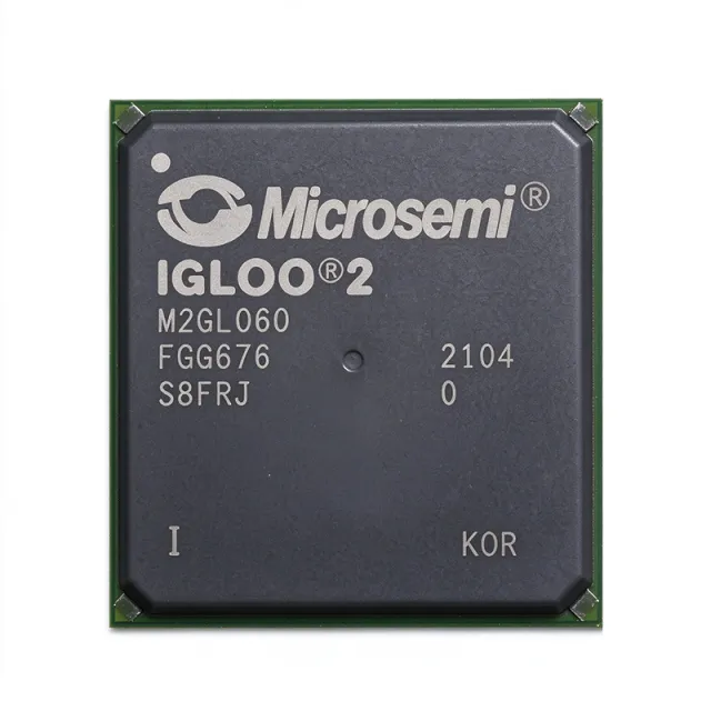
Microchip Technology M2GL060-FG676 is an IGLOO 2 low-density flash field-programmable gate array with 56.5K logic elements, 387 I/O, and a 1.2 V core supply in a 676-ball FBGA package. The device is offered in a commercial 0°C to 85°C temperature grade and is listed as in production by Microchip. Its combination of programmable logic, embedded flash configuration, and 387 package I/O positions supports general-purpose bridging, I/O expansion and conversion, system management, secure connectivity, communications, industrial, medical, defense, and aviation designs. An FPGA is a reprogrammable semiconductor in which configurable logic blocks, memory resources, and programmable I/O form a hardware system that can be modified after manufacture. Within the semiconductor hierarchy, an FPGA sits above programmable logic devices and below application-specific programmable systems. The IGLOO 2 family is specifically designed for low-density, nonvolatile flash-based programmable logic rather than fixed-function application-specific integrated circuits. The M2GL060-FG676 provides 56,520 logic cells according to distributor records, with a separate product listing identifying 56.5K logic elements. Its 387 I/O positions provide extensive board-level connectivity, while the 1.2 V core voltage identifies the device as intended for modern low-voltage digital designs. Configuration is nonvolatile because the IGLOO 2 family uses embedded flash, allowing the programmed design to remain available after power removal without an external configuration PROM. The 676-ball FBGA package makes the M2GL060-FG676 suitable for compact, multilayer PCB assemblies where perimeter lead counts would be restrictive. Its 0°C to 85°C commercial temperature range covers many indoor industrial, communications, medical, and consumer-adjacent systems. Unlike a mask-programmed ASIC, the FPGA allows logic, interfaces, and system-management functions to be revised through configuration changes, which can reduce prototype iteration and support product differentiation. Typical uses include protocol bridging, parallel-to-serial interface conversion, Ethernet or USB interface support, control-plane logic, data acquisition, industrial control, and embedded security functions. The 387 I/O count is particularly useful when a design must connect multiple buses, sensors, converters, and status signals while retaining flexible programmable logic for control and protocol handling. PCB implementation requires careful BGA layout and thermal engineering. Designers should follow Microchip's FG676 pin-information guide and the referenced board-and-layout guidelines, provide all required power and ground connections, and validate high-speed signal integrity across the multilayer stackup. Because the verified excerpt does not state the complete pin map, voltage tolerances, performance grade, or recommended high-speed capacitor values, those details must be checked against the manufacturer datasheet before release. This product page consolidates verified distributor and manufacturer information, documented application roles, procurement status, and engineering-selection guidance. It distinguishes the target from higher-density IGLOO 2 devices and avoids presenting unsupported electrical, timing, pricing, or package details as confirmed facts.

Cotización Contacto
M2GL060-FG676I - 56.5K LEs Industrial FPGA | Microchip
M2GL060-FG676I

M2GL060-FG676I - 56.5K LEs Industrial FPGA | Microchip

The Microchip Technology M2GL060-FG676I is an IGLOO 2 low-density FPGA with 56,520 logic elements, 387 I/O, and a 676-BGA package. It is identified as an industrial-grade device with an operating temperature range of -40°C to 100°C junction temperature and a core supply range of 1.14 V to 2.625 V. The device supports general-purpose bridging, I/O expansion, conversion, system-management, and secure-connectivity functions. An FPGA is a programmable semiconductor whose logic, interconnect, and I/O resources are configured after manufacture. In the device hierarchy, the M2GL060-FG676I belongs to the IGLOO 2 family, combines the low-density FPGA product class, and sits within the broader integrated-circuit and programmable-logic markets. This distinction matters because an FPGA can implement parallel control, protocol, interface, and signal-processing functions without changing the physical PCB when logic requirements evolve. The device provides 56,520 logic elements and 387 I/O in a 676-ball BGA package. Its 1.14 V to 2.625 V operating-voltage range supports low-voltage digital core implementations, while the industrial temperature rating extends operation beyond typical commercial temperature conditions. The 676-BGA format provides a large ball count and fine interconnect pitch, enabling the high I/O density required by complex communications, industrial, and embedded-control systems. The M2GL060-FG676I is a flash FPGA, allowing its configuration to be stored and restored without a separate external configuration device. Its architecture is intended for general-purpose logic functions rather than application-specific signal processing. Designers can use programmable logic for bus bridging, protocol conversion, I/O expansion, supervisory functions, and secure connectivity, provided that each interface is assigned to a compatible voltage bank and satisfies the device's timing and power requirements. Typical deployments include industrial automation controllers, communications equipment, embedded system-management logic, and bridging subsystems. In these systems, the FPGA is useful when several parallel interfaces or protocol converters must be consolidated into one programmable device. A 387-I/O device also supports designs that need substantial external connectivity while preserving a single, high-density package. PCB implementation requires careful BGA layout, power-plane planning, and high-speed routing discipline. Designers should follow the IGLOO 2 Packaging and Pin Descriptions User Guide for ball assignments, voltage-bank mapping, and mechanical dimensions. Configuration storage, clocking, decoupling, and JTAG access should be validated against the device programming and clocking guidance before release to production. This product record combines the manufacturer device information, package characteristics, lifecycle status, and verified cross-reference findings with practical selection guidance. It supports engineers comparing the M2GL060-FG676I against other IGLOO 2 package variants while preserving the strict requirement that a drop-in alternative use the same 676-BGA footprint and remain pin-compatible.

Cotización Contacto
M2GL060-FGG484 - 56.5K Logic Cells | Microchip | Industrial
M2GL060-FGG484

M2GL060-FGG484 - 56.5K Logic Cells | Microchip | Industrial

The Microchip Technology M2GL060-FGG484 is an IGLOO 2 flash-based field-programmable gate array with 56,520 logic elements, 267 user I/Os, and a 1.2 V operating supply in a 484-ball FBGA package. It is designed for compact, low-power programmable logic in industrial, communications, medical, defense, and aviation systems. The device combines a reusable nonvolatile configuration architecture with 267 I/Os, allowing designers to implement protocol bridging, I/O expansion, interface conversion, video and image processing, system management, and secure connectivity without relying on an external configuration device. An FPGA is a programmable semiconductor whose logic fabric, interconnect network, and peripherals can be configured after fabrication. This makes the FPGA hierarchy broader than a fixed-function logic IC. The M2GL060-FGG484 belongs to the IGLOO 2 low-density FPGA family, where flash configuration memory provides a practical single-chip implementation for moderate logic density. Its 267 I/Os provide substantial board-level connectivity, while the 484-ball FBGA supports dense routing in space-constrained equipment. The headline implementation advantages are the 56,520 logic elements, 267 user I/Os, and 1.2 V supply requirement. These figures allow complex control paths, parallel data processing, and multiple external interfaces to coexist in one device. The M2GL060-FGG484 is particularly useful when a design needs more flexibility than an application-specific controller but does not justify the power, cost, and complexity of a much larger FPGA. Its surface-mount 484-ball package also supports automated assembly and high-density PCB layouts. Microchip positions IGLOO 2 devices for general-purpose functions including Gigabit Ethernet or dual PCI Express control planes, bridging, I/O expansion and conversion, image processing, system management, and secure connectivity. Because configuration is stored in flash, the device can support deterministic startup behavior without a separate configuration PROM. Engineers should still account for configuration pins, dedicated programming resources, bank voltage constraints, and the pin requirements of their selected interfaces when planning the PCB. Typical uses include industrial communication gateways, medical monitoring equipment, defense and aviation subsystems, video-capture interfaces, secure network access equipment, and embedded control systems. The device can consolidate multiple fixed-function logic blocks into one programmable implementation, simplifying board partitioning and allowing firmware or configuration updates during product maintenance. Its low-density positioning makes it well matched to control-plane logic, sensor aggregation, and protocol translation rather than large parallel-compute workloads. A key design consideration is that the complete BGA pin assignment, bank architecture, and electrical constraints must be taken directly from the manufacturer pin-description guide. Confirm every power, ground, configuration, clock, and user-I/O connection before layout release. High-speed interfaces also require disciplined return-path planning, while the 1.2 V core supply requires a regulator and decoupling network designed for the device's transient requirements. This page consolidates the manufacturer's device identity, family application guidance, lifecycle status, package information, and verified cross-reference information. It also provides parameter-level comparisons, drop-in migration notes, and practical design guidance for engineers evaluating the M2GL060-FGG484 against same-family speed and temperature-grade options.

Cotización Contacto
M2GL060-FGG676 - 56.5K Logic Cells, 387 I/O FPGA | Microchip Technology
M2GL060-FGG676

M2GL060-FGG676 - 56.5K Logic Cells, 387 I/O FPGA | Microchip Technology

Microchip Technology M2GL060-FGG676 is an IGLOO2 flash-based field-programmable gate array with 56,520 logic cells, 387 user I/Os and a 676-ball BGA package. The device operates from a 1.2 V core supply and is specified for applications up to 85 °C. Its high logic-cell count and extensive I/O resources make it suitable for general-purpose programmable logic, bridging, I/O expansion, conversion, system management and secure connectivity functions. An FPGA is a programmable semiconductor containing configurable logic fabric, memory resources and programmable I/O. Within the product hierarchy, the M2GL060-FGG676 is an FPGA and CPLD, a programmable-logic device, and ultimately a semiconductor. Unlike a fixed-function controller, its internal configuration can be changed to implement different control, data-routing and interface functions on the same board design. The IGLOO2 architecture combines 56,520 logic cells with 387 I/O and approximately 1,826 kb of RAM as listed for the related M2GL060-FGG676I ordering code. A 1.2 V core supply supports low-voltage digital operation, while the 676-BGA package provides a large, fine-pitch connection interface. The 1 mm terminal pitch and 676 terminals make careful PCB layout, thermal management and assembly planning essential. The device is suitable for communications, industrial and embedded systems where logic density, I/O availability and programmable functionality are more important than very low unit cost. Common design roles include protocol bridging, legacy interface conversion, peripheral aggregation, system supervision, secure data control and industrial control logic. Its broad I/O count allows multiple external buses and discrete signals to be consolidated into a single programmable device. Designers should select the appropriate I/O voltage, bank configuration and power architecture from the manufacturer datasheet before layout begins. The BGA footprint requires via-in-pad or via-under-bump design rules, and the power grid should be evaluated for the required logic activity and temperature range. Because the exact public pin table is not reproduced here, use the Microchip IGLOO2 Packaging and Pin Descriptions User Guide when assigning every ball and bank. This product page combines the manufacturer product resources, distributor listings, cross-reference findings and practical implementation guidance to support device selection. The M2GL060-FGG676 is best suited to designs that require the 676-BGA footprint, 56,520 logic cells and 387 I/Os in a low-power flash-based FPGA.

USD $180,47 En stock
M2GL060-VF400 - 56.5K LE IGLOO2 FPGA | Microchip Technology
M2GL060-VF400

M2GL060-VF400 - 56.5K LE IGLOO2 FPGA | Microchip Technology

Microchip Technology M2GL060-VF400 is an IGLOO2 low-density flash FPGA with 56,520 logic elements, 207 I/O, and a 400-LFBGA package. It is designed for embedded applications requiring programmable logic, bridging, I/O expansion, system management, secure connectivity, and general-purpose control functions. The device combines a reprogrammable FPGA fabric with embedded memory resources and on-chip flash in a single low-power package. According to the verified manufacturer listing, the M2GL060 device family is in production, and the M2GL060-VF400 is specifically identified as a 400-pin LFBGA FPGA with 207 I/O. The IGLOO2 family targets communications, industrial, medical, defense, and aviation applications, where configurable logic can reduce the component count and accelerate prototype development compared with fixed-function logic. The 1.2 V operating value shown in the verified distributor data reflects the device’s low-voltage architecture, while the 400-terminal square ball-grid package supports dense PCB routing and high I/O availability. Engineers should select this part when the design requires substantially more logic and I/O than the smaller M2GL005 and M2GL010 devices, but does not justify moving to a different FPGA family. Production design work requires the Microchip IGLOO 2 FPGA and SmartFusion 2 SoC FPGA datasheet, the IGLOO 2 Packaging and Pin Descriptions User Guide, and the appropriate device programming and verification toolchain. Pin assignments, bank voltages, configuration behavior, and package dimensions must be checked against those authoritative documents before schematic capture or PCB layout release.

Cotización Contacto
M2GL060-VF400I - 56.5K LEs, 400-BGA FPGA | Microchip
M2GL060-VF400I

M2GL060-VF400I - 56.5K LEs, 400-BGA FPGA | Microchip

The Microchip Technology M2GL060-VF400I is a low-density IGLOO2 flash-based field-programmable gate array with 56.5K logic elements, 207 I/O, and a 400-pin VFBGA package. The device operates from a 1.2 V core supply and integrates 32 KB of embedded SRAM with high-performance communications interfaces. Its fourth-generation flash-based FPGA fabric makes it suitable for programmable logic, bridging, I/O expansion, conversion, system management, and secure connectivity functions. An FPGA is a reconfigurable digital semiconductor in which the logic, routing, and I/O behavior are defined after fabrication. Within the semiconductor hierarchy, the M2GL060 belongs to the programmable-logic device class, combining a configurable logic fabric, embedded memory, and peripheral interfaces on one integrated circuit. This integration allows one device to replace combinations of fixed-function logic, often reducing board area and simplifying product revisions. The IGLOO2 family combines non-volatile configuration storage with programmable logic. A 400-pin VFBGA package provides extensive board-level connectivity, while 207 I/O positions support interfaces to external memories, converters, communications circuits, and control peripherals. The 56.5K logic-element count gives the design substantial parallel processing capacity without moving to a larger FPGA architecture. On-chip configuration flash also allows the device to retain its programmed logic during normal power-off operation. Microchip describes the M2GL060 as an in-production device for cost-optimized FPGA applications. The product family targets communications, industrial, medical, defense, and aviation markets, including Gigabit Ethernet or dual PCI Express control planes, bridging, video and image processing, I/O conversion, system management, and secure connectivity. These applications benefit from programmable hardware that can be updated without changing the PCB when field requirements evolve. The 400-pin package requires careful signal-integrity and layout planning. Designers should preserve the device's recommended power and ground distribution, use manufacturer-referenced ball assignments, and confirm that external interfaces match the selected bank voltage. Because the package exposes 207 I/O positions, connector density, bank assignment, and high-speed routing can determine whether a particular board layout fits the target application. Before finalizing a design, verify the exact M2GL060-VF400I ordering code, supported I/O standards, speed grade, temperature grade, and power requirements against the Microchip datasheet and packaging user guide. A hardware-equivalent suffix does not necessarily preserve every commercial or environmental qualification, so confirm the complete part number before committing it to a production BOM. This product summary combines the manufacturer family documentation, packaging guidance, device status, and manufacturer ordering information with practical considerations for PCB implementation, qualification, and sourcing. It is intended to accelerate early architecture decisions while directing detailed verification to the authoritative Microchip documents.

Cotización Contacto
M2GL060-VFG400 - 56.5K Logic Cells FPGA | Microchip
M2GL060-VFG400

M2GL060-VFG400 - 56.5K Logic Cells FPGA | Microchip

The Microchip Technology M2GL060-VFG400 is an IGLOO2 low-density FPGA with 56,500 logic elements, 207 I/O, and a 400-LFBGA package. It integrates a fourth-generation flash-based FPGA fabric with high-performance communications interfaces on a single chip. The device is designed for low-cost, low-power programmable logic applications that benefit from non-volatile configuration and a broad set of general-purpose connectivity functions. An FPGA is a programmable semiconductor whose logic fabric, interconnect, and I/O can be configured after manufacture. Within the device hierarchy, the M2GL060-VFG400 belongs to the IGLOO2 family of flash-based FPGAs, which sits below the broader field-programmable gate array and programmable-logic categories. Flash configuration retains the programmed logic image when power is removed, allowing systems to resume operation without a separate configuration PROM. The M2GL060-VFG400 provides 56.5K logic elements, 207 user I/O, and an embedded memory subsystem that includes on-chip flash, 32 KB embedded SRAM, and multiple DMA controllers. Its communications-oriented architecture supports applications such as bridging, I/O expansion and conversion, system management, secure connectivity, video and image processing, and industrial control. The 400-LFBGA package supports dense board-level integration while exposing the substantial I/O count required by programmable-logic designs. Microchip describes the IGLOO2 family as targeting cost-optimized FPGA markets while combining fourth-generation flash-based logic with high-performance communications interfaces. Because the M2GL060 is a low-density member, it is appropriate when a design needs substantial programmable logic but does not require the resources of a larger FPGA. Its non-volatile configuration also helps simplify boot behavior in equipment that must operate immediately after power restoration. Typical applications include protocol bridging, industrial interface conversion, embedded system management, secure communications, video and image processing, and general-purpose I/O expansion. A board-level design can place the FPGA between processors or sensors and fieldbus networks, allowing parallel data paths, timing constraints, and protocol conversion to be implemented in programmable logic. The 207-I/O count is especially useful for systems that must accommodate multiple buses, control signals, and high-speed data interfaces. A critical design consideration is that BGA routing, power distribution, decoupling, and programming-tool compatibility must be evaluated before committing the 400-LFBGA footprint to a PCB. Use the IGLOO 2 FPGA Packaging and Pin Descriptions User Guide to assign banks and verify package constraints, and use the IGLOO 2 FPGA and SmartFusion 2 SoC FPGA Datasheet for electrical and functional limits. Software and bitstream compatibility should also be confirmed for the exact device identifier. This product record combines the manufacturer device information with distributor and cross-reference findings to provide practical selection context. It also organizes the verified FPGA resources, package information, alternatives, applications, and design cautions needed to plan an IGLOO2-based board without relying on a single catalog entry.

Cotización Contacto
M2GL060T-FG484 - 56.5K LEs, 267 I/O Flash FPGA | Microchip
M2GL060T-FG484

M2GL060T-FG484 - 56.5K LEs, 267 I/O Flash FPGA | Microchip

The Microchip Technology M2GL060T-FG484 is a 56.5K logic-element IGLOO2 low-density flash FPGA with 267 I/O in a 484-ball BGA package. It combines reconfigurable programmable logic, embedded flash, and 32 KB of embedded SRAM for general-purpose control, bridging, I/O expansion, video and image processing, secure connectivity, Gigabit Ethernet, and dual PCI Express control-plane designs. A flash FPGA is a programmable-logic semiconductor whose configuration memory is embedded on the die. Unlike a CPLD, an FPGA provides substantially greater logic capacity and supports parallel datapath, state-machine, interface-conversion, and signal-processing architectures. The IGLOO2 family is positioned within the broader hierarchy of FPGA devices, programmable logic ICs, and semiconductor devices for embedded control and interface acceleration. The M2GL060T-FG484 provides 56.5K logic elements and 267 I/O, making it useful for consolidating multiple fixed-function interface blocks onto one programmable device. Its embedded flash allows the configuration to be retained in the package, while the embedded SRAM supports buffering, datapath storage, and general-purpose logic. The 484-BGA format offers a high pin count for dense external connectivity and can help reduce the number of discrete interface components in bridge and protocol-conversion designs. Typical deployments include Gigabit Ethernet control planes, dual PCI Express control-plane functions, protocol bridging, I/O expansion, bus-width conversion, system management, secure connectivity, and video or image-processing pipelines. In these applications, the FPGA can implement deterministic parallel logic while the integrated flash simplifies standalone configuration management. A primary design consideration is the 484-ball BGA layout. PCB escape routing, via-in-pad or via-under-ball requirements, soldering process capability, and thermal performance must be validated before layout begins. Designers should also verify the exact supported I/O standards, voltage domains, clocking resources, configuration requirements, and power rails against the manufacturer datasheet for the selected board revision. This page combines the device architecture, verified package and capacity details, drop-in package alternatives, application guidance, and practical PCB considerations into an engineering-focused resource. It helps designers distinguish suffix and qualification options without changing the physical 484-ball footprint and compare same-density IGLOO2 alternatives before committing to a layout.

Cotización Contacto
M2GL060T-FG676 - 56.5K Logic Cells IGLOO2 FPGA | Microchip
M2GL060T-FG676

M2GL060T-FG676 - 56.5K Logic Cells IGLOO2 FPGA | Microchip

The Microchip Technology M2GL060T-FG676 is an IGLOO 2 low-density flash FPGA with 56.5K logic elements, 387 I/O, and a 676-ball FBGA package. It is designed for general-purpose programmable logic, system management, bridging, I/O expansion and conversion, video or image processing, and secure connectivity functions. The device combines embedded flash configuration memory with a low-power programmable-logic fabric, allowing the implemented circuit to be retained without continuous external configuration loading. An FPGA is a programmable semiconductor containing configurable logic blocks, programmable interconnect resources, and input/output circuitry. Unlike a fixed-function application-specific integrated circuit, an FPGA can be programmed after manufacture for a defined control, interface, datapath, or system-management function. The M2GL060T-FG676 belongs to the IGLOO 2 family and provides 56.5K logic elements and 387 I/O in the 676-FBGA package identified by the FG676 ordering code. The 387-I/O count provides a large external interface capacity for parallel buses, control signals, data acquisition, communication interfaces, and mixed logic systems. The 676-ball FBGA package supports dense board routing in compact equipment but requires careful PCB layout, power delivery, thermal management, and assembly-process control. The integrated flash configuration feature is useful where the final logic configuration must be stored locally and loaded without an external configuration device. Typical uses include Gigabit Ethernet or PCI Express control-plane logic, protocol bridging, I/O expansion and conversion, video and image processing, embedded system management, and secure connectivity. These applications benefit from parallel programmable resources and a large pin count, although design partitioning, timing closure, and resource utilization remain important engineering considerations. When planning a PCB around the M2GL060T-FG676, follow the manufacturer package outline, ball map, and recommended power and ground layouts exactly. Confirm that the assembly process supports the 676-FBGA geometry, inspectability requirements, and solder mask or paste design rules. Route high-speed or sensitive interfaces according to the applicable Microchip guidance rather than treating the device as a conventional low-pin-count FPGA. This product page combines the confirmed device identity and manufacturer application positioning with package-specific design guidance, replacement considerations, and structured comparison information. It is intended to help engineers confirm fit, plan PCB implementation, and evaluate compatible configuration or speed-grade alternatives before releasing a design to production.

Cotización Contacto
M2GL060T-VF400 - 56.5K IGLOO2 FPGA | Microchip Technology
M2GL060T-VF400

M2GL060T-VF400 - 56.5K IGLOO2 FPGA | Microchip Technology

Microchip Technology M2GL060T-VF400 is a low-density IGLOO2 flash FPGA with 56,520 logic elements, 207 I/O pins, and a 400-pin VFBGA package. The device operates from a 1.2 V supply and is designed for general-purpose programmable-logic functions including bridging, I/O expansion, system management, secure connectivity, image processing, and communication interfaces. An FPGA is a programmable semiconductor in which the digital logic, interconnect, and many I/O functions are defined through a configuration bitstream. Within the product hierarchy, the M2GL060T-VF400 is a low-density FPGA in the IGLOO2 family, combining reconfigurable logic with nonvolatile flash configuration memory. This makes it useful when a design needs hardware flexibility, rapid prototyping, or a field-updatable logic implementation without replacing a fixed-function ASIC. The M2GL060T-VF400 provides 56,520 logic elements, 207 I/O, and a 1.2 V operating supply in a surface-mount 400-VFBGA package. Its 207 available I/O positions make the device especially suitable for systems requiring substantial parallel connectivity. The manufacturer identifies IGLOO2 devices for bridging functions, I/O expansion and conversion, system management, secure connectivity, Gigabit Ethernet or dual PCI Express control planes, and video or image processing. The IGLOO2 architecture supports programmable digital logic in a compact package. Because the configuration is stored in flash, the device does not require a separate external configuration PROM for normal operation. Engineers can use the Microchip programming toolchain to implement the design, compile it, and program the FPGA, while the many I/O pins allow external memory, communications, sensors, and control signals to interface directly with the programmable core. Typical uses include industrial control, medical instrumentation, communications equipment, defense and aviation electronics, Ethernet or PCIe interface logic, protocol conversion, sensor aggregation, and embedded system management. Its 207 I/O count can simplify designs that would otherwise require several smaller programmable devices or a larger ASIC development cycle. A 400-VFBGA package requires careful PCB layout and assembly planning. Follow the manufacturer pinout, recommended power and ground planes, and decoupling guidance in the IGLOO2 datasheet. Verify the selected flash configuration and pin assignment before release, especially when the design depends on a specific I/O voltage, differential interface, or high-speed routing arrangement.

Cotización Contacto
M2GL090-1FG484 - 86K Logic Cell FPGA | Microchip
M2GL090-1FG484

M2GL090-1FG484 - 86K Logic Cell FPGA | Microchip

The Microchip Technology M2GL090-1FG484 is an IGLOO2 low-density field-programmable gate array with 86,316 programmable logic cells, 267 I/O, a 1.2 V core supply, and a 484-pin FBGA package. It combines programmable logic, embedded flash configuration storage, and high-density user I/O in a single surface-mount device. The M2GL090 is listed by Microchip as In Production and is positioned for general-purpose functions such as bridging, I/O expansion, conversion, system management, and secure connectivity. An FPGA is a programmable semiconductor whose internal logic and interconnect resources can be configured after manufacture. The M2GL090 belongs to the IGLOO2 family, placing it within the hierarchy of flash-based FPGA, programmable logic device, digital semiconductor, and integrated circuit. Its 484-ball grid array package provides substantial connectivity compared with smaller leaded packages, making it suitable for designs requiring numerous external signals and board-level integration. The device provides 86,316 logic cells and 267 I/O according to distributor and manufacturer listings. Its core operating voltage is 1.2 V. These resources make the M2GL090 useful for protocol bridging, data acquisition, industrial control logic, communications interfaces, and embedded system-management functions. Microchip identifies communications and industrial applications as principal markets for Microchip FPGAs, while the M2GL090 product page highlights bridging, I/O expansion, conversion, system management, and secure connectivity use cases. The M2GL090-1FG484 belongs to the low-density IGLOO2 portfolio and is available from multiple distributors, indicating an established supply channel. Its 484-pin FBGA construction requires careful PCB layout because the fine ball pitch constrains routing, inspection, and rework. A valid design therefore depends on accurate package data, a qualified assembly process, and power, ground, configuration, and interface verification in the Libero design flow. Typical deployments include industrial data-acquisition modules, communications bridges, embedded control systems, I/O concentrators, and secure connectivity products. Because the verified material does not provide complete power-consumption, operating-temperature, clock, memory, or signal-timing tables, those values should be confirmed in the applicable Microchip IGLOO2 documentation before schematic approval or production release. The principal design consideration is package-level implementation. Engineers should use the official IGLOO2 484-pin package and pin-description material to assign power, ground, configuration pins, and user I/O correctly. Decoupling, layer-stackup, via density, ball-pad geometry, and assembly capability should be reviewed early because those constraints can drive PCB cost and yield. This page consolidates the verified manufacturer status, distributor availability, device-family specifications, and same-package procurement alternatives. It also distinguishes electrically identical ordering codes from changes that affect qualification or sourcing, providing practical information for FPGA selection, PCB reuse, BOM standardization, and supply-chain review.

Cotización Contacto
M2GL090-1FG676 - 86K IGLOO2 FPGA with 425 I/O | Microchip
M2GL090-1FG676

M2GL090-1FG676 - 86K IGLOO2 FPGA with 425 I/O | Microchip

The Microchip Technology M2GL090-1FG676 is an IGLOO2 field-programmable gate array with 86,316 cells, 425 I/O, a 1.2 V operating supply, and a 676-ball FBGA package. It is designed for compact programmable-logic systems requiring substantially more routing and I/O capacity than small CPLDs. The device is supplied in a tray according to the verified distributor data. An FPGA is a digital semiconductor whose logic, interconnects, and I/O behavior are configured after manufacture. In the device hierarchy, an FPGA sits above fixed-function logic and below application-specific SoCs. Its reconfigurable fabric allows designers to implement parallel processing, control logic, protocol handling, signal conditioning, and interface bridging in one device while shortening board-development cycles. The M2GL090 belongs to the IGLOO2 family and is identified as a low-density FPGA offering 86K logic elements. Its 425 I/O provide substantial board-level connectivity, while the 1.2 V supply specification identifies it as a modern low-voltage programmable-logic device. The 676-ball FBGA package supports fine-pitch, high-density assembly but requires careful PCB layout, via-in-pad-compatible manufacturing, and thermal analysis. Technically, the IGLOO2 architecture is suited to designs that benefit from reconfigurable hardware rather than repeated firmware changes alone. The verified component listings identify 86,316 cells, 425 I/O, and the M2GL090 series designation. Detailed RAM, flash, PLL, I/O-standard, security, and performance values are not included in the supplied source data and should be confirmed in the official M2GL090 documentation before design release. Typical uses include industrial control, factory automation, communications infrastructure, embedded instrumentation, and compact control systems that need many parallel I/O and moderate programmable-logic density. The large I/O count can also simplify connections among sensors, relays, converters, memory, and external processors when board space is constrained. The primary design consideration is PCB manufacturability. A 676-ball FBGA requires a fine-pitch land pattern, adequate solder-mask and paste control, and power and ground distribution that minimizes voltage drop. Designers should also verify every bank supply, configuration interface, and I/O standard against the official packaging and pin-description guide. This page consolidates verified distributor specifications, an exact industrial-temperature variant, same-family drop-in candidates, comparison parameters, and practical assembly guidance. It extends the basic catalog data with design-focused context while clearly separating verified facts from parameters that still require manufacturer-document confirmation.

Cotización Contacto
M2GL090-1FGG484 - 86K LEs, 267 I/O, 1.2V IGLOO2 FPGA
M2GL090-1FGG484

M2GL090-1FGG484 - 86K LEs, 267 I/O, 1.2V IGLOO2 FPGA

The Microchip Technology M2GL090-1FGG484 is an IGLOO2 low-density FPGA with 86,316 logic elements, 267 user I/O, and a 1.2 V operating supply in a 484-ball FBGA package. It provides programmable logic resources for bridging, I/O expansion and conversion, system management, secure connectivity, communications, industrial control, and embedded video or image processing. The -1 suffix denotes the manufacturer's speed grade, while FGG484 identifies the 484-ball package configuration. An FPGA is a reconfigurable digital semiconductor whose internal look-up tables, flip-flops, routing resources, memory blocks, and programmable I/O can be configured after manufacture. The M2GL090 belongs to the IGLOO2 hierarchy: low-density FPGA, programmable logic device, integrated circuit, and semiconductor. This positioning makes it suitable for consolidating control logic, protocol conversion, and interface adaptation that would otherwise require multiple discrete programmable or glue-logic devices. The principal device figures are 86,316 logic elements, 267 user I/O, and a 1.2 V supply voltage. Its broad I/O count is valuable for systems requiring numerous digital connections, while the logic capacity supports parallel control, data acquisition, packet handling, and interface bridging. Unlike a fixed-function microcontroller, the FPGA can adapt its internal architecture and pin behavior when the system design changes, reducing external logic and shortening development cycles. Microchip positions IGLOO2 devices for general-purpose functions including Gigabit Ethernet or dual PCI Express control planes, bridging, input/output expansion and conversion, video and image processing, system management, and secure connectivity. The M2GL090 family is therefore appropriate when deterministic parallel logic, flexible I/O, and post-configuration modification are more important than the simplicity of a software-only control path. Typical applications include industrial protocol converters, camera and imaging interfaces, secure network-edge equipment, automated test systems, embedded control panels, and communications infrastructure. The 267-I/O device can consolidate high-pin-count interfaces, although each design still requires bank-specific voltage planning, power sequencing, and careful PCB escape routing around the FBGA array. A key design consideration is migration from smaller IGLOO2 devices. The same 484-ball package can be used across M2GL025, M2GL050, and M2GL090 families, but global-pin availability differs, so unused globals must be checked explicitly in the package pin-description guide. Power, interface standards, and FPGA timing constraints should also be evaluated before reusing a board across density grades. This page combines manufacturer and distributor lifecycle information, package and logic specifications, drop-in family alternatives, application guidance, and migration-oriented design notes. It is intended to help engineers identify the correct IGLOO2 density, package, and speed-grade combination without overlooking differences in temperature rating, suffix coding, or device configuration.

Cotización Contacto
M2GL090-FCS325 - 86K LEs, 180 I/O Flash FPGA | Microchip
M2GL090-FCS325

M2GL090-FCS325 - 86K LEs, 180 I/O Flash FPGA | Microchip

The Microchip Technology M2GL090-FCS325 is an IGLOO 2 low-density flash FPGA with 86K logic elements, 180 I/O, and a 325-TFBGA package. The device combines programmable logic, embedded memory resources, and configuration flash in a single integrated circuit intended for general-purpose logic, bridging, I/O expansion, data conversion, system management, and secure connectivity applications. An FPGA, or field-programmable gate array, is a programmable logic semiconductor whose digital circuits are defined through a hardware description rather than a fixed mask set. The M2GL090 belongs to the IGLOO 2 hierarchy of flash FPGAs, which sit within the broader programmable-logic and semiconductor categories. This makes the device suitable for designs that require adjustable interfaces, parallel processing, protocol adaptation, or system-control logic while retaining a low-density footprint. The IGLOO 2 family provides on-chip flash, embedded SRAM, and multiple DMA controllers for applications that move data between programmable logic and external interfaces. Its 86K logic-element capacity gives designers substantially more implementation flexibility than small programmable logic devices, while the 180 I/O count supports dense board-level connections. On-chip flash supports nonvolatile configuration, and the embedded SRAM enables fast working storage for data processing and interface buffering. The 325-TFBGA package provides a high-density interconnect solution for multilayer printed circuit boards. Ball assignment and electrical characteristics must be checked against the Microchip IGLOO 2 datasheet and package drawing before layout begins. Because a 325-ball package contains many power, ground, configuration, clock, and general-purpose I/O connections, board planning should include uninterrupted supply distribution, careful escape routing, and thermal-aware placement. Typical uses include industrial bridging and protocol conversion, control-plane logic for communications equipment, I/O expansion, general data acquisition, video and image processing, secure system management, and medical or defense equipment. The IGLOO 2 family is specifically positioned for functions such as Gigabit Ethernet or dual PCI Express control planes, bridging, I/O expansion and conversion, video and image processing, system management, and secure connectivity. Designers should begin with the IGLOO 2 package pinout, identify the required banks and voltage domains, and confirm device operating parameters against the datasheet. The 180 I/O figure describes the maximum device I/O resource rather than permitting every package ball to be used as an unrestricted user signal. Bank voltage, configuration pins, dedicated clock pins, and power requirements determine the usable logic interface in a specific design. This product page combines the M2GL090 device identity, 86K logic-element capacity, 180 I/O count, 325-TFBGA package information, family-level application guidance, candidate ordering-code comparisons, and practical implementation considerations. It is designed to help engineers identify the correct IGLOO 2 variant and move directly to the manufacturer data sheet and package documentation before beginning schematic capture or PCB layout.

Cotización Contacto
M2GL090-FG484 - 86K LEs IGLOO2 FPGA, 484 FBGA | Microchip Technology
M2GL090-FG484

M2GL090-FG484 - 86K LEs IGLOO2 FPGA, 484 FBGA | Microchip Technology

The Microchip Technology M2GL090-FG484 is an IGLOO2 low-density flash FPGA with 86,316 logic elements, 267 I/O, and a 484-ball FBGA package. The device is identified by distributor listings as an IGLOO2 Field Programmable Gate Array with 86K LEs and 1.2 V operation, making it suitable for embedded control, interface bridging, I/O expansion, system management, and secure connectivity applications. An FPGA is a programmable digital semiconductor that combines configurable logic, programmable interconnect, and programmable I/O in one device. The IGLOO2 family is a flash-based FPGA family, allowing configuration data to be stored in the device and supporting general-purpose functions such as protocol bridging, data conversion, control-plane logic, and system supervision. The M2GL090-FG484 sits at the higher end of the listed low-density IGLOO2 options, providing substantially more logic resources than smaller M2GL005, M2GL010, M2GL025, or M2GL050 devices. The verified device information identifies 86,316 FPGA cells, 267 I/O, a 1.2 V supply, and a 484-pin FBGA package with a 23 mm by 23 mm body and 1 mm pitch. The Microchip IGLOO2 family is documented for communications, industrial, medical, defense, and aviation markets. The same package family is used across several IGLOO2 density options, although Microchip application note AC402 notes that some pins have reduced compatibility between M2GL025, M2GL050, and M2GL090 devices in the FG484 package. Typical designs use the M2GL090-FG484 for moderate-complexity embedded systems requiring multiple interfaces, custom protocol conversion, control logic, data acquisition, or secure connectivity. The 267 I/O count provides a broad interface surface for parallel buses, memory interfaces, control signals, and communications peripherals. Designers should still verify the exact bank assignments, voltage standards, configuration requirements, and pin multiplexing for the selected board revision using the manufacturer pin-information documentation. For migration within the FG484 family, footprint compatibility does not automatically guarantee identical functionality. AC402 specifically identifies reduced compatibility for some pins across the M2GL025, M2GL050, and M2GL090 devices. The device should therefore be selected against the complete pin-description table, power architecture, and design migration application note rather than by package name alone. This product data combines manufacturer family information, distributor specifications, package references, and cross-reference findings. It distinguishes the target M2GL090-FG484 from related density, speed-grade, temperature-grade, and package-ordering variants, helping engineers evaluate whether a candidate is genuinely drop-in compatible before changing a PCB or production BOM.

Cotización Contacto
M2GL090-FG484I - 86K LEs, 267 I/O IGLOO2 FPGA | Microchip
M2GL090-FG484I

M2GL090-FG484I - 86K LEs, 267 I/O IGLOO2 FPGA | Microchip

Microchip Technology M2GL090-FG484I is an IGLOO2 low-density flash FPGA with 86K logic elements, 267 I/O, and a 484-ball BGA package. The device operates at 1.2 V and is supplied in the industrial temperature grade. Its in-production status and broad general-purpose logic resources make it suitable for interface conversion, I/O expansion, bridging, system management, and secure connectivity designs. The M2GL090 family is positioned within the FPGA and CPLD hierarchy as a reprogrammable logic semiconductor combining configurable logic, embedded flash configuration memory, and a high-density ball-grid-array footprint. An FPGA is a programmable semiconductor whose logic fabric and I/O behavior can be configured after manufacture. The IGLOO2 family is a flash FPGA family from Microchip Technology, which combines low-power programmable logic with embedded configuration storage. Within the broader semiconductor hierarchy, an FPGA is a programmable logic device that sits above basic fixed-function logic ICs and alongside CPLDs. This distinction matters when a design needs reconfigurable parallel logic, numerous interface pins, or product-level logic changes without a conventional ASIC fabrication cycle. The verified product data identifies 86K logic elements, 267 I/O, 1.2 V operation, 484-ball BGA construction, and industrial temperature grading. The large pin count provides substantial connectivity for buses, converters, control signals, and external memory interfaces. The 1.2 V core supports low-voltage logic implementations, while the embedded flash architecture allows configuration data to be retained without a separate external configuration PROM. Exact I/O standards, supported memory interfaces, PLL resources, and fabric performance figures are not present in the supplied excerpts and therefore require confirmation in the complete Microchip documentation. The IGLOO2 architecture is intended for general-purpose programmable logic rather than a single fixed function. The M2GL090 is described by Microchip as a low-density FPGA, and its 86K logic-element count provides substantially more design capacity than small CPLDs. This capacity is useful for combining multiple interface blocks, control logic, and protocol adaptation in one device. Because the verified excerpts do not disclose the complete speed-grade, static-power, dynamic-power, or timing tables, designs should not assume a particular frequency until the selected device, package, and speed grade are checked against the manufacturer data sheet. Typical uses include bridging functions, I/O expansion, data and protocol conversion, system management, secure connectivity, and industrial communications. The 267 available I/O positions are particularly valuable when a design connects several differently standardized buses or translates wide parallel interfaces into serial links. The same device family is also used in communications, industrial, medical, defense, and aviation markets. These applications benefit from programmable logic that can implement multiple protocol and timing functions without relying on a large collection of dedicated glue devices. PCB design should prioritize the 484-ball BGA escape-routing strategy, clean supply distribution around the 1.2 V core, and verified I/O voltage compatibility for every connected interface. Although the BGA package supports dense integration, it requires careful via-in-pad or buried-via routing, appropriate solder-mask and paste design, and thermal analysis for sustained industrial operation. Designers should also confirm the exact pin assignments and bank power requirements in the Microchip IGLOO 2 FPGA Packaging and Pin Descriptions User Guide before releasing the layout. This product record combines verified distributor and manufacturer information, same-family drop-in candidates, package-specific comparison data, and practical FPGA design guidance. It distinguishes confirmed facts from parameters that still require confirmation from the complete manufacturer data sheet, helping engineers narrow the replacement and sourcing process without treating incomplete search snippets as authoritative specifications.

Cotización Contacto
M2GL090-FG676 - 86K IGLOO2 FPGA, 1.2V, 676-FBGA | Microchip
M2GL090-FG676

M2GL090-FG676 - 86K IGLOO2 FPGA, 1.2V, 676-FBGA | Microchip

The Microchip M2GL090-FG676 is an IGLOO2 low-density FPGA with 86,316 logic cells, 425 I/O, a 1.2 V supply, and a 676-pin FBGA package. It is designed for programmable logic, system management, bridging, I/O expansion, data conversion, and secure connectivity applications. The verified distributor data identifies the device as an 86KLE IGLOO2 FPGA, while the manufacturer product page reports the M2GL090 family as in production. An FPGA is a programmable semiconductor whose logic fabric, interconnect, and programmable I/O can be configured after manufacture. Unlike a fixed-function ASIC, an FPGA supports design changes, parallel interface adaptation, and hardware customization without changing the PCB. The M2GL090 belongs to the IGLOO2 family, which is positioned for general-purpose programmable-logic functions and low-density embedded control tasks. The M2GL090-FG676 provides 86,316 logic cells and 425 I/O in a 676-pin FBGA. The verified distributor listing also shows a 2,648,064-bit configuration-memory figure for this device. Its 1.2 V operating supply is suitable for designs requiring a low-voltage programmable-logic fabric. The FG676 package provides a high pin count and supports dense signal routing, although its fine-pitch land pattern demands careful PCB layout and assembly. IGLOO2 devices include programmable logic resources and embedded SRAM for designs requiring local data storage, buffering, or stateful logic. Depending on the device configuration, the FPGA can be used for protocol conversion, bus bridging, control logic, interface aggregation, and security-related connectivity. The exact supported I/O standards, voltage combinations, timing grades, and configuration features must be confirmed in the Microchip datasheet for the selected device variant. Typical implementations include industrial control modules, communications equipment, data-acquisition systems, sensor and network interfaces, embedded security functions, and custom accelerator logic. In these systems, the FPGA can absorb parallel data paths, perform protocol translation, implement deterministic state machines, and reduce the amount of logic that would otherwise require several fixed-function devices. PCB design is a primary concern for the 676-pin FBGA. Use the Microchip IGLOO 2 layout guidance, provide a continuous power and ground distribution structure, route high-speed signals with controlled impedance, and verify the pin assignments and ball-grid orientation against the official pin-description document. Programming and configuration must follow the device-specific requirements. This product record combines verified manufacturer and distributor information with package-specific engineering guidance. Because the supplied search data does not include a complete pricing table, electrical limits, temperature grade, or full pin map, those values are explicitly marked for verification rather than inferred.

Cotización Contacto
M2GL090-FG676I - 86K LEs, 425 I/O IGLOO2 FPGA | Microchip
M2GL090-FG676I

M2GL090-FG676I - 86K LEs, 425 I/O IGLOO2 FPGA | Microchip

The Microchip Technology M2GL090-FG676I is an IGLOO2 low-density FPGA with 86,000 logic elements, 425 I/O, and a 676-ball BGA package. It is identified by the verified product data as an IGLOO2 Field Programmable Gate Array intended for industrial temperature-grade applications. The M2GL090 family combines programmable logic resources with embedded FPGA fabric and is positioned for general-purpose functions such as bridging, I/O expansion, system management, and secure connectivity. An FPGA is a semiconductor device whose digital logic, interconnect, and I/O behavior are configured after manufacture. The IGLOO2 family belongs to the broader field-programmable logic hierarchy: FPGA > programmable logic device > digital semiconductor. Unlike a fixed-function microcontroller, the M2GL090 can implement parallel control, protocol conversion, data acquisition, interface bridging, and other digital logic functions in one integrated device. Its 676-BGA package provides a high pin count for demanding external connectivity and board-level integration. The verified distributor listings identify the M2GL090-FG676I as an 86K-logic-element IGLOO2 FPGA with 425 I/O and a 676-BGA package. The related M2GL090-1FG676I is likewise listed with 425 I/O and 86K logic elements, supporting comparison with a same-footprint speed- or ordering variant. Microchip’s M2GL090 product page describes the family as suitable for communications, industrial, and general-purpose embedded applications, including bridging functions, I/O expansion, system management, and secure connectivity. The 676-ball BGA package is appropriate when a design requires numerous high-density board connections, but it also increases PCB layout and inspection complexity. Designers should preserve the manufacturer’s ball assignments and power, ground, configuration, and I/O guidance from the IGLOO2 packaging and pin-information document. The package is surface-mount technology and is not a through-hole package, so its land pattern and assembly process must match the selected 676-ball package variant. Typical deployments include industrial interface bridges, communications equipment, data-conversion systems, embedded control modules, secure-connectivity infrastructure, and general-purpose I/O expansion. For these applications, the M2GL090-FG676I is selected when designers need a low-density, high-pin-count programmable logic platform rather than a fixed microcontroller. The exact timing, voltage, temperature, power, configuration, and I/O electrical limits should be confirmed in the Microchip IGLOO2 datasheet before schematic signoff or PCB release. This page consolidates the verified Microchip and distributor information for engineering comparison, identifies same-footprint replacement candidates, and adds practical package, sourcing, and design guidance that is not found in a bare distributor listing. It is intended to support initial design decisions while preserving the manufacturer datasheet as the authoritative source for final electrical and timing requirements.

Cotización Contacto
M2GL090-FGG484 - FPGAs | Microsemi | Embedded Systems
M2GL090-FGG484

M2GL090-FGG484 - FPGAs | Microsemi | Embedded Systems

The Microsemi Corporation M2GL090-FGG484 is an M2GL-series field-programmable gate array intended for programmable digital logic and embedded-system applications. Its supplied order code identifies the FGG484 package variant, but the verified retrieval did not return a manufacturer specification table, pin list, pricing record, lifecycle statement, or substitute cross-reference. Consequently, resource counts, I/O quantities, voltage ranges, performance, temperature grades, and package dimensions remain unverified and are not presented as confirmed specifications. A field-programmable gate array, or FPGA, is a semiconductor whose digital logic is configured after manufacture. Within the broader product hierarchy, an FPGA is a programmable logic device, a semiconductor, and an embedded-processing component. This distinction matters because an FPGA can implement parallel control logic, protocol interfaces, signal processing, or general-purpose digital functions, depending on the resources and interfaces specified by the manufacturer for the exact device. The M2 designation identifies the M2GL product family, while FGG484 is the manufacturer ordering suffix for this particular configuration. No verified data in the supplied record establishes whether the suffix denotes package type, environmental grade, lead-free status, temperature range, or a combination of ordering attributes. Those details should therefore be confirmed from the official ordering guide before schematic capture, footprint selection, or component approval. For design evaluation, engineers should obtain the official M2GL090 data sheet, package drawing, pinout, and errata. The principal checks are the number and location of general-purpose I/O pins, supported I/O standards, available logic and memory resources, configuration interface requirements, and the electrical limits associated with the intended core and I/O supply voltages. Those details control whether an existing board can accept the device without changes. Potential uses include industrial control, communications infrastructure, instrumentation, embedded vision, and test equipment. These are application categories rather than verified manufacturer recommendations because the supplied data contains no application note or reference-design list. Selection must be based on the full electrical and mechanical data for M2GL090-FGG484 after those documents are obtained. The primary design precaution is to avoid deriving PCB, power, or thermal conclusions from the order code alone. In particular, do not assume a ball count, land pattern, I/O voltage, or junction-temperature limit from the 484 suffix. Confirm those items against the package drawing and data sheet, and validate the power budget across every supported configuration and operating-temperature condition. This page deliberately separates the confirmed identity from missing technical evidence, marks unavailable specifications explicitly, and provides a structured framework for datasheet review, sourcing, comparison, and drop-in replacement analysis. That approach reduces procurement and design risk when the live distributor and manufacturer retrieval contains no usable technical records.

Cotización Contacto
M2GL090-FGG676 - 86K LEs, 1.2V, 676-FBGA FPGA | Microchip
M2GL090-FGG676

M2GL090-FGG676 - 86K LEs, 1.2V, 676-FBGA FPGA | Microchip

The Microchip Technology M2GL090-FGG676 is an IGLOO2 low-density FPGA with 86,316 logic elements, 425 user I/O, and a 1.2 V core supply in a 676-pin FBGA package. It is a surface-mount programmable-logic device intended for general-purpose functions such as bridging, I/O expansion, conversion, system management, and secure connectivity. An FPGA is a semiconductor whose digital logic is configured after manufacture, allowing one physical device to implement multiple control, interface, and data-processing functions. The M2GL090 belongs to the IGLOO2 family, a low-density FPGA family positioned between simple programmable logic devices and larger FPGAs. Its combination of 86,316 logic elements and 425 I/O makes it suitable for systems requiring substantial parallel connectivity without moving to a higher-density device. The verified product information identifies the device as an IGLOO2 low-density FPGA with 86K logic elements, 425 I/O, 1.2 V operation, and a 676-pin FBGA package. The Microchip manufacturer page lists the M2GL090 family as in production. The FGG676 ordering code is associated with the 676-pin surface-mount package, while detailed speed-grade, temperature-grade, memory, and I/O-standard information is not available in the supplied verified excerpts. This device is suitable for industrial communications equipment, embedded control, peripheral expansion, sensor aggregation, and secure-connectivity implementations. Its high pin count provides extensive board-level connectivity, while the 86K logic-element density provides more implementation capacity than basic glue-logic devices. The manufacturer specifically identifies bridging, I/O expansion, conversion, system management, and secure connectivity as representative applications. Designers should treat the 676-pin FBGA as a demanding fine-pitch package requiring controlled PCB design, assembly, and inspection. Power, decoupling, configuration-data integrity, and I/O-standard compatibility must be reviewed against the complete Microchip datasheet and pin-information guide before release to manufacturing. Because the supplied data does not expose a complete price or full parametric table, the listing distinguishes confirmed facts from fields requiring datasheet confirmation. This page consolidates the verified manufacturer and distributor information for M2GL090-FGG676, including package identity, logic density, I/O count, lifecycle indication, source links, and same-package replacement guidance. It also provides engineering-oriented application and design guidance without treating unverified speed, temperature, pricing, or electrical limits as established facts.

Cotización Contacto
M2GL090T-1FG484 - 86K FPGA, 267 I/O, 484-BGA | Microchip
M2GL090T-1FG484

M2GL090T-1FG484 - 86K FPGA, 267 I/O, 484-BGA | Microchip

Microchip Technology M2GL090T-1FG484 is an IGLOO2 flash FPGA in a 484-BGA package with 86,316 logic cells, 267 I/O, and a 1.2 V device rating. It is designed for general-purpose programmable logic, including Gigabit Ethernet, dual PCI Express control planes, bridging, I/O expansion and conversion, video or image processing, system management, and secure connectivity. The IGLOO2 family is a flash-based field-programmable gate array architecture. Unlike mask-programmable logic devices, an FPGA can be configured after manufacture, allowing a design to be revised during prototyping, production, or field updates. The M2GL090T device provides programmable logic resources alongside dedicated I/O, making it suitable for systems that need flexible interface handling, protocol bridging, and control logic in one package. The M2GL090T-1FG484 provides 86,316 logic cells, 267 I/O, and 1.2 V operation according to the product listings and manufacturer family information. Its 484-BGA package provides a large, high-density footprint suitable for multilayer PCB layouts and designs requiring numerous external connections. The device is identified as an IGLOO2 FPGA with flash configuration support and is available in multiple orderable suffix variants. Typical applications include Gigabit Ethernet interface logic, PCI Express control-plane functions, protocol bridging, system management, secure connectivity, video and image processing, and industrial control systems. The high I/O count is particularly useful when several buses, converters, memory interfaces, or discrete signals must be consolidated into programmable logic. PCB implementation requires careful BGA escape routing, power and ground-plane integrity, and compliance with the manufacturer’s decoupling and layout guidance. BGA escape routing, via-in-pad construction, thermal management, and high-speed signal integrity determine whether the device operates reliably at its intended clock and I/O rates. Use the manufacturer pin-description table when assigning signals and the IGLOO2 hardware design guidance for power, clock, configuration, and JTAG connections. This page combines the exact MPN identifiers, package information, programming context, and application guidance needed to evaluate the M2GL090T-1FG484 against related IGLOO2 options. The part is best distinguished from alternatives by its exact package suffix, temperature-grade coding, configuration method, and orderable MPN rather than by cell count alone.

Cotización Contacto
M2GL090T-FG484 - 86K Cell 1.2V Flash FPGA | Microchip
M2GL090T-FG484

M2GL090T-FG484 - 86K Cell 1.2V Flash FPGA | Microchip

The Microchip Technology M2GL090T-FG484 is an IGLOO2 flash FPGA with 86,316 logic cells, 267 I/O, and a nominal 1.2 V core supply in a 484-pin FBGA package. It combines reprogrammable nonvolatile configuration storage with an embedded programmable-logic fabric for general-purpose control, interface, bridging, conversion, video and image processing, and secure connectivity functions. The M2GL090 device combines 86,316 logic cells with 267 available I/O to support integration of multiple fixed-function blocks into a single FPGA implementation. Its 484-pin FBGA package provides a high pin count for parallel interfaces and external memory connections. The 1.2 V supply is the nominal core operating voltage identified in the manufacturer product data; detailed voltage limits, timing grades, and current budgets must be confirmed in the device documentation. Unlike mask-programmable logic or SRAM-only FPGAs, the IGLOO2 family stores its configuration in flash, allowing the device to retain its programmed logic after power is removed. An FPGA is a user-programmable semiconductor whose digital logic blocks, routing resources, and I/O cells are configured to implement custom hardware functions. Within the broader semiconductor hierarchy, an FPGA is a programmable-logic device, while the IGLOO2 belongs to the low-density flash-FPGA segment of the Microchip product portfolio. It is intended for designs where parallel logic, protocol conversion, control-plane processing, or system-management functions benefit from hardware-level configurability and shorter development cycles than application-specific ASIC development. Key features include 86,316 logic cells, 267 I/O, embedded flash configuration, and a 1.2 V nominal core supply. The large I/O count makes the device suitable for parallel control interfaces, bus bridging, I/O expansion, and protocol conversion. Its nonvolatile configuration supports field updates without requiring a separate configuration SRAM, while the high-pin-count FBGA package can reduce external glue logic when many signals must leave the device. Microchip identifies the IGLOO2 family for Gigabit Ethernet or dual PCI Express control planes, bridging, I/O expansion and conversion, video and image processing, system management, and secure connectivity. The device architecture is organized around programmable logic elements, programmable interconnect, user I/O, dedicated configuration resources, and embedded flash memory. Configuration is retained in flash, so startup behavior does not depend on an external configuration loader for normal operation. Design migration within the M2GL025, M2GL050, and M2GL090 devices using the FG484 package is addressed by Microchip application note AC402, although each migration still requires checking speed grade, temperature grade, voltage, resource utilization, pin constraints, and board-level compatibility. The target suffix “T” denotes the ordering configuration shown in the verified results, while the exact commercial and temperature classifications should be checked against the ordering information. Typical applications include Gigabit Ethernet control-plane logic, dual PCI Express control-plane functions, data and protocol bridging, parallel-to-serial or serial-to-parallel conversion, industrial I/O expansion, video and image-processing pipelines, secure-connectivity hardware, and general system-management controllers. The 267-I/O device is particularly useful where many independent digital channels must terminate on one programmable component, while the embedded flash configuration allows field-programmable behavior to be updated without volatile reload through an external programmer. A key design consideration is package and migration validation. Before reusing an existing FG484 layout, engineers should review the IGLOO2 Packaging and Pin Descriptions User Guide and application note AC402, verify power rails and I/O standards, and confirm that the selected device provides every required bank and peripheral connection. Differential, high-speed, clock, configuration, and supply pins must also satisfy the manufacturer’s routing and decoupling guidance. This product record consolidates verified manufacturer and distributor information, identifies same-package family alternatives, compares ordering variants, and adds practical migration and design guidance. It separates confirmed facts from unavailable pricing, lifecycle, compliance, and detailed timing information so engineers can review the appropriate manufacturer documents before committing a design to production.

Cotización Contacto