Productos (39.000+)

M2GL090T-FG484I - 86K LLE IGLOO2 FPGA | Microchip
M2GL090T-FG484I

M2GL090T-FG484I - 86K LLE IGLOO2 FPGA | Microchip

The Microchip Technology M2GL090T-FG484I is an IGLOO2 low-density field-programmable gate array with 86,316 programmable logic cells, 267 I/O, a 1.2 V operating supply, and a 484-BGA package. It is a flash-configurable FPGA designed for general-purpose control, bridging, I/O expansion, video and image processing, system management, secure connectivity, Gigabit Ethernet, and dual PCI Express control-plane functions. An FPGA is a programmable semiconductor whose configurable logic blocks and I/O can be interconnected to implement digital systems. The IGLOO2 family belongs to the broader FPGA and CPLD hierarchy within programmable logic devices. By retaining configuration data in flash, the M2GL090T-FG484I supports systems that need field-updatable logic without external configuration memory. The device provides 86,316 logic cells, equivalent to the 86K LLE class, together with 267 I/O. Its 1.2 V operating supply and 484-ball BGA package make it appropriate for compact, high-pin-count industrial, communications, and embedded-control designs. The -1 suffix identifies a particular device grade, while the trailing I denotes the industrial-temperature option associated with the MPN. Microchip positions the M2GL090T family for programmable control-plane logic, protocol bridging, I/O conversion and expansion, video or image processing, and secure-connectivity functions. The large I/O count provides substantial connectivity for parallel interfaces, memory interfaces, control signals, and high-speed programmable I/O. Its 484-BGA footprint also demands careful PCB layout, power delivery, via-in-pad consideration, and thermal verification. Typical designs include Gigabit Ethernet interface logic, dual PCI Express control-plane blocks, industrial protocol converters, image-processing pipelines, system-management controllers, and secure networking equipment. The 267 I/O count is particularly useful when a design must combine multiple bus interfaces, data conversion functions, and supervisory logic in one programmable device. Designers should use the manufacturer pinout and package information when assigning BGA balls and planning power planes. Differential pairs, high-speed interfaces, and sensitive clocks require controlled impedance and return-path continuity. Thermal analysis must include the package, PCB copper, vias, airflow, and the power dissipated by the configured logic rather than relying on a generic FPGA thermal estimate. This page combines the confirmed device resources, package, temperature range, and application roles with a drop-in comparison, practical PCB guidance, and structured selection criteria. It is intended to help engineers determine whether the M2GL090T-FG484I fits a specific programmable-logic design before reviewing the detailed manufacturer documentation.

Cotización Contacto
M2GL090T-FG676 - 86K LEs, 425 I/O FPGA | Microchip | Industrial
M2GL090T-FG676

M2GL090T-FG676 - 86K LEs, 425 I/O FPGA | Microchip | Industrial

The Microchip Technology M2GL090T-FG676 is a low-density IGLOO 2 flash FPGA with 86,316 logic elements, 425 I/O, and a 1.2 V core in a 676-pin FBGA package. It combines programmable logic with embedded flash configuration memory and is intended for general-purpose bridging, I/O expansion, conversion, system management, and secure connectivity functions. The device is supplied in tray packaging under the exact manufacturer ordering code M2GL090T-FG676. An FPGA is a reconfigurable semiconductor whose logic blocks, memory resources, and I/O can be programmed after manufacture. Within the product hierarchy, the M2GL090T-FG676 is an IGLOO 2 FPGA, a low-density member of the IGLOO family, and a member of the broader FPGA and programmable-logic semiconductor category. Unlike a fixed-function application-specific integrated circuit, an FPGA can implement multiple interface or control functions in one device while retaining field-updatable configuration through embedded flash. The verified product information identifies 86K logic elements, 86,316 total FPGA cells, 425 I/O, a 1.2 V supply classification, and a 676-pin FBGA package. The large I/O count makes the device particularly useful at the boundary between external systems and programmable logic. Its 676-ball grid also provides dense signal access, but it requires a correspondingly complex PCB footprint, careful escape routing, and assembly-level process control. Configuration data can remain local in the device's embedded flash, reducing the need for a separate configuration PROM in designs that use the non-volatile configuration feature. M2GL090 devices are positioned for bridging functions, input/output expansion and conversion, system management, and secure connectivity. Manufacturer product information for the M2GL090T family also identifies Gigabit Ethernet and dual PCI Express control-plane use cases. The distinction between M2GL090T-FG676 and related M2GL090 order codes lies primarily in the ordering-code suffix, while exact electrical, temperature, and timing limits must be confirmed against the manufacturer documentation for the specific suffix. The verified distributor records consistently identify the target as an IGLOO 2 FPGA with 425 I/O and a 676-BGA package. Typical deployments include industrial protocol bridges, parallel-to-serial interface conversion, embedded control planes, FPGA-based I/O expansion, and secure connectivity gateways. The 425-I/O device is particularly attractive when the board architecture requires many independently programmable digital interfaces but does not justify a higher-density or higher-power FPGA. Such designs benefit from deterministic programmable logic and the ability to revise configuration without replacing the device. The main design consideration is package complexity. A 676-pin FBGA requires via-in-pad or otherwise carefully implemented escape routing, fine-pitch assembly capability, adequate solder-mask and paste control, and extensive continuity and boundary-scan validation. Designers should also verify the exact pinout, bank voltage rules, configuration pins, clocking resources, and supported I/O standards against the IGLOO 2 packaging and pin-description user guide before schematic release. This page consolidates verified distributor pricing, package information, same-family drop-in candidates, comparison parameters, and practical implementation guidance. It distinguishes verified facts from parameters that require confirmation, helping engineers evaluate the M2GL090T-FG676 without confusing a package-compatible ordering-code variant with a functionally and electrically identical part.

Cotización Contacto
M2GL090T-FGG484 - 86K-LE IGLOO2 FPGA | Microchip Technology
M2GL090T-FGG484

M2GL090T-FGG484 - 86K-LE IGLOO2 FPGA | Microchip Technology

The Microchip Technology M2GL090T-FGG484 is a 1.2 V IGLOO2 low-density field-programmable gate array with 86,316 logic elements, 267 I/O, and a 484-ball FBGA package. It combines reprogrammable digital logic with embedded flash configuration memory in a surface-mount package intended for industrial, communications, embedded, and secure-connectivity systems. An FPGA is a semiconductor whose digital logic, I/O behavior, and interfaces are configured after manufacture. Within the device hierarchy, the M2GL090T belongs to the IGLOO2 family of low-density FPGAs, which sits below higher-density programmable logic and above fixed-function logic devices. Its combination of logic resources, programmable I/O, and embedded flash makes it useful for control-plane logic, protocol bridging, data acquisition, system management, and hardware security functions. Key features include 86,316 logic elements, 267 I/O, and a 1.2 V operating supply. The 484-ball FBGA package provides a high pin count for designs requiring numerous external connections, while surface mounting supports compact, high-density boards. The IGLOO2 architecture is specifically positioned for general-purpose bridging, I/O expansion and conversion, video or image processing, system management, and secure connectivity. The M2GL090T-FGG484 provides a practical migration path within the Microchip IGLOO2 portfolio. Devices identified by the IGLOO2 family and 484-ball package share a common platform, but ordering suffixes can distinguish temperature grade, speed grade, or qualification status. Design migration should therefore compare the complete ordering code, I/O assignments, power requirements, timing constraints, and the target Libero design rather than relying on the base device name alone. Typical uses include Gigabit Ethernet or dual PCI Express control planes, protocol converters, sensor and data-acquisition interfaces, industrial automation controllers, video capture helpers, secure boot and key-management support, and general-purpose glue logic. These applications benefit from flexible I/O assignment and parallel programmable logic in a single nonvolatile device. Board design requires careful attention to the 1.2 V power rail, decoupling, BGA escape routing, clock integrity, and I/O standards. Use the manufacturer’s pin-description guide to assign every ball and confirm that adjacent high-speed or sensitive pins meet the required layout constraints. Program the device through the supported Microchip programming and development environment. This page combines device specifications, ordering-code comparisons, package considerations, and practical selection guidance. It helps engineers distinguish true drop-in options from variants that differ in temperature, speed, qualification, or lifecycle requirements before committing a 484-ball design to production.

Cotización Contacto
M2GL090T-FGG676 - 86K Logic Element IGLOO2 FPGA | Microchip
M2GL090T-FGG676

M2GL090T-FGG676 - 86K Logic Element IGLOO2 FPGA | Microchip

The Microchip Technology M2GL090T-FGG676 is an IGLOO2 flash field-programmable gate array with 86,316 logic elements, 425 I/O, and a 1.2 V core voltage in a 676-ball BGA package. It combines programmable logic resources with nonvolatile configuration memory in a single device suitable for communications, industrial, embedded, and system-management equipment. An FPGA is a semiconductor whose digital circuitry can be configured after manufacture to implement control logic, interfaces, protocol handling, datapaths, and other digital functions. Within the product hierarchy, an FPGA sits above fixed-function logic and below a programmable SoC. Unlike a mask-programmed ASIC, an FPGA allows its interconnect and logic configuration to be revised during development, which can shorten prototype cycles and support field updates when the device includes suitable configuration and update resources. The M2GL090T-FGG676 provides 86,316 logic elements and 425 I/O according to the manufacturer product information. Its flash-based configuration architecture supports nonvolatile FPGA operation, while its large I/O count offers extensive connectivity for external memory, control signals, serial interfaces, and parallel buses. The 676-ball BGA package supports dense board layouts but requires careful escape routing and multilayer PCB construction. The device operates from a 1.2 V core according to the published comparison information, with the manufacturer using the IGLOO2 architecture for general-purpose logic functions. Available I/O count and performance depend on the selected device, package, speed grade, configuration, and design constraints. Engineers should therefore treat the M2GL090T-FGG676 as a programmable-logic platform rather than as a fixed peripheral block. Typical uses include Gigabit Ethernet control-plane logic, dual PCI Express control planes, bridge and protocol-conversion functions, I/O expansion, video and image processing, system management, and secure connectivity. These applications map well to the combination of 86,316 logic elements and 425 I/O because they require flexible parallel logic, multiple external interfaces, and design updates without changing the PCB. The principal design considerations are power sequencing, decoupling, configuration handling, signal integrity, thermal performance, and BGA layout execution. Because this is a 676-ball package, use the manufacturer pin-description tables and package drawings to assign every ball, power bank, and I/O standard before PCB routing. Keep high-speed and sensitive interfaces away from noisy power regions and follow the recommended reference-decoupling network. This product page combines the manufacturer's application positioning, package and logic-resource facts, sourcing options, drop-in candidate analysis, and practical PCB guidance into one engineering-focused reference. It also distinguishes confirmed direct alternatives from broader FPGA choices so designers can assess replacement risk before committing a new layout.

Cotización Contacto
M2GL150-FCS536 - 146K IGLOO2 FPGA | Microchip Technology
M2GL150-FCS536

M2GL150-FCS536 - 146K IGLOO2 FPGA | Microchip Technology

The Microchip Technology M2GL150-FCS536 is an IGLOO2 flash-based field-programmable gate array with 146,124 logic elements, 512,000 RAM bits, and 293 I/O in a 536-LFBGA CSPBGA package. It combines programmable logic, embedded RAM, and high I/O density for bridging, protocol conversion, I/O expansion, system management, secure connectivity, communications, industrial, medical, defense, and aviation systems. An FPGA is a reconfigurable digital semiconductor in which programmable logic blocks, memory resources, and I/O cells are configured after manufacture. The M2GL150 belongs to Microchip Technology's IGLOO2 family, a hierarchy that connects field-programmable logic to general-purpose programmable logic devices and embedded semiconductor solutions. Flash configuration support makes the device suitable for designs that require persistent programmed behavior across power cycles. The M2GL150-FCS536 provides 146,124 programmable logic elements and 512,000 RAM bits, giving designers substantial parallel-processing and data-storage flexibility. Its 293 I/O support is particularly useful in space-constrained systems requiring high connectivity. The device is identified as a low-density IGLOO2 FPGA, while the manufacturer describes the broader M2GL150 family as intended for general-purpose functions such as bridging, I/O expansion and conversion, system management, and secure connectivity. Compared with a fixed-function application-specific integrated circuit, an FPGA permits design changes through programmable logic rather than a new mask set. This can accelerate system customization, interface adaptation, and product differentiation. The trade-off is higher device complexity and the need to configure the logic correctly for timing, power, and I/O requirements. Typical applications include interface bridges, data converters, control-plane logic, industrial automation, communications equipment, medical systems, and secure connectivity. In a bridging design, the 293 available I/O can support multiple external interfaces, while the 146,124 logic elements can implement protocol state machines, data paths, and control functions in parallel. PCB implementation requires careful attention to the 536-ball BGA escape routing, power distribution, clocking, and high-speed signal integrity. Use the Microchip IGLOO2 Packaging and Pin Descriptions User Guide to assign every ball and observe the package-specific layout guidance in application note AN4153. This product page combines manufacturer status information, package and resource counts, documented use cases, compatible family members, and practical implementation guidance. It helps engineers identify the correct device while separating true same-package alternatives from options that require a different footprint or design qualification.

Cotización Contacto
M2GL150-FCV484 - 146K LE IGLOO2 FPGA | Microchip
M2GL150-FCV484

M2GL150-FCV484 - 146K LE IGLOO2 FPGA | Microchip

The Microchip Technology M2GL150-FCV484 is an IGLOO2 low-density field-programmable gate array with 146,124 logic elements, 248 I/O, 5,120,000 bits of embedded flash memory, and a 1.2 V operating supply in a 484-pin BFBGA package. It combines programmable logic, embedded nonvolatile memory, and 248 general-purpose I/O in a single device intended for general-purpose FPGA functions. An FPGA is a programmable digital semiconductor whose logic fabric can be configured after manufacture. The M2GL150-FCV484 belongs to the IGLOO2 family, which sits within the broader field-programmable logic and semiconductor hierarchy. Its embedded flash supports configuration and system logic, while its large I/O count makes it useful for bridges, interface conversion, system management, secure connectivity, and control-plane functions that require numerous external connections. The device combines 146,124 logic elements with 248 I/O and a 484-pin ball-grid-array package. The embedded memory capacity is listed as 5,120,000 bits, allowing designs to combine control logic with nonvolatile data storage. Its 1.2 V core supply is appropriate for low-density, embedded programmable-logic systems where low core voltage and integrated configuration memory are valuable. The manufacturer lists the M2GL150 family as being in production. The FCV484 package provides a high pin count and a dense board footprint. Unlike a simple fixed-function logic device, the FPGA can support multiple interface standards through programmable I/O, serializing engines, embedded memory, and external bus bridges. The 248 available I/O are particularly useful when a design must connect multiple bus widths, control signals, status indicators, or communication channels without using several companion devices. Typical uses include Gigabit Ethernet or dual PCI Express control-plane logic, industrial interface bridges, I/O expansion, protocol conversion, embedded control, and secure connectivity. The Microchip IGLOO 2 portfolio specifically identifies general-purpose functions such as bridging, I/O expansion, conversion, system management, and secure connectivity as suitable workloads. PCB implementation requires careful BGA fanout, power-plane construction, ground distribution, and high-speed routing discipline. Use the package drawing and pin-description guide when assigning balls, and follow Microchip's board and layout guidance for IGLOO 2 and SmartFusion 2 designs. Differential and high-speed interface paths should use matched routing geometry, continuous reference planes, and carefully placed decoupling. This product page combines manufacturer status information, package and resource details, pinout resources, drop-in migration candidates, and practical implementation guidance. It is intended to help engineers identify the correct IGLOO 2 density, package, temperature grade, and speed grade before committing a new PCB or migrating an existing design.

Cotización Contacto
M2GL150-FCVG484I - IGLOO2 146K LE FPGA 484-BGA | Microchip
M2GL150-FCVG484I

M2GL150-FCVG484I - IGLOO2 146K LE FPGA 484-BGA | Microchip

The Microchip Technology M2GL150-FCVG484I is a 146,124-logic-element IGLOO2 low-power flash-based Field-Programmable Gate Array (FPGA) integrated circuit housed in a 484-ball Fine-pitch Ball Grid Array (FBGA, 19x19 mm) package with 248 user I/O. Built on a 1.2 V core, 65 nm flash process, the device combines up to 5,120 Kbits of embedded SRAM, 240 Math Blocks (18x18 multipliers), 4 PLLs and DLLs, and 1.2 Gbps SERDES capability, addressing low-density logic integration and high-speed serial bridging without an external MCU. An FPGA (Field-Programmable Gate Array) is a semiconductor device built around an array of configurable logic blocks (CLBs) connected by programmable interconnect, allowing designers to customize digital functions after fabrication. FPGAs sit in the hierarchy: programmable logic -> logic IC -> integrated circuit -> semiconductor. The IGLOO2 family specifically targets low-power operation with flash-based configuration cells that retain bitstream in silicon without external boot memory, simplifying board design and improving security. Key features include 512 Kbits of embedded non-volatile memory (eNVM), 64 KB embedded SRAM (eSRAM), high-performance DDR2/DDR3/LPDDR memory controller interfaces with ECC, integrated DSP through the Math Block array, and an ARM Cortex-M3 hard processor subsystem variant (M2GL150S). The I/O count of 248 supports wide parallel interfaces for video bridging, industrial control and communications aggregation. The flash-based architecture provides instant-on capability and inherent security against bitstream read-back, advantages over SRAM-based FPGAs that require external boot PROMs. From a technical depth perspective, the M2GL150 uses a 4-input LUT fabric with dedicated carry chains and distributed control logic, providing a fine-grained architecture suitable for glue logic, bus bridging and signal conditioning. The 65 nm low-power process node enables sub-microamp sleep currents and flexible power modes that suit battery-powered and industrial always-on applications. Typical applications include industrial control planes, secure communications bridges, motor control and I/O expansion, video/image processing, and low-power system management. The flash-based non-volatile configuration makes the device particularly attractive for safety-critical and secure systems requiring deterministic boot and tamper resistance. When designing, ensure the PCB layout accommodates the 484-ball FBGA 19x19 mm land pattern with controlled-impedance traces for SERDES lanes and matched-length DDR routing for memory interfaces. Heat dissipation is generally low due to flash-based operation, but core utilization above 70 percent may require thermal analysis. This page synthesizes distributor pricing, drop-in alternatives, and practical design notes not found in the manufacturer datasheet.

Cotización Contacto
M2S010-TQG144 - SmartFusion2 SoC FPGA 12K LE 166MHz | Microchip
M2S010-TQG144

M2S010-TQG144 - SmartFusion2 SoC FPGA 12K LE 166MHz | Microchip

The Microchip Technology M2S010-TQG144 is a SmartFusion2 System-on-Chip (SoC) FPGA integrating a 166 MHz ARM Cortex-M3 hard processor subsystem with a flash-based FPGA fabric of approximately 12,000 logic elements (10K logic modules / 12KLEs), housed in a 144-pin TQFP package (20x20 mm). The device combines deterministic FPGA logic, an embedded microcontroller, and advanced security features on a single low-power 65 nm process die, targeting secure connectivity, industrial control, and general-purpose I/O expansion designs. A SmartFusion2 SoC FPGA is a heterogeneous computing device that fuses a hard ARM Cortex-M3 processor core, on-chip SRAM and eNVM, debug peripherals, and a reprogrammable FPGA fabric in one package. This integration removes the inter-chip communication latency of a discrete MCU-plus-FPGA design and simplifies the PCB by collapsing what would otherwise be a multi-chip system onto a single 144-TQFP footprint. M2S010 sits at the low-density end of the SmartFusion2 family, with larger siblings (M2S025, M2S050, M2S060, M2S150) scaling up logic and memory. Key features of M2S010-TQG144 include 12KLEs / 12084 cells of flash-based FPGA fabric, a 166 MHz ARM Cortex-M3 subsystem, on-chip 512 KB eNVM and 64 KB SRAM, embedded DDR controllers, multiple high-speed serial transceivers, and hardware cryptographic accelerators for AES, SHA, and ECC. The device operates from a 1.2 V core supply and supports industrial temperature grades, with low static and dynamic power consumption enabled by flash-based non-volatile configuration cells. Typical applications include industrial motor control, secure IoT edge nodes, communications bridging, system management controllers, and PCI Express endpoint designs. The integrated ARM Cortex-M3 allows designers to host control-plane firmware on-chip while the FPGA fabric handles high-bandwidth data-plane logic, data acquisition, or custom peripheral glue logic.

Cotización Contacto
M2S025-VFG400I - SmartFusion2 SoC FPGA, 25K LE, Cortex-M3 | Microchip
M2S025-VFG400I

M2S025-VFG400I - SmartFusion2 SoC FPGA, 25K LE, Cortex-M3 | Microchip

The Microchip Technology M2S025-VFG400I is a SmartFusion2 System-on-Chip (SoC) FPGA integrating a 25K-logic-element flash-based FPGA fabric with a hard ARM Cortex-M3 microcontroller subsystem running at 166 MHz, housed in a 400-ball VFBGA (17x17 mm) package. Built on a low-power 65 nm flash process, the device delivers approximately 27,696 logic cells, embedded SRAM, DSP blocks, and high-speed serial transceivers while embedding the deterministic ARM Cortex-M3 processor alongside programmable analog. A System-on-Chip (SoC) FPGA is an integrated device that combines a programmable logic fabric with one or more fixed processor cores and, in many families, programmable analog. The hierarchy places SoC FPGA under FPGA & CPLD and alongside conventional microcontroller units. SmartFusion2 specifically integrates a flash FPGA, a deterministic Cortex-M3 hard processor, and an analog compute engine, allowing designers to consolidate what previously required a microcontroller, an FPGA, and a separate ADC-plus-front-end chip onto a single die. Key features of the M2S025 include 43 kbits of embedded SRAM, dedicated DSP blocks, multi-standard SERDES, on-chip user flash, hard Cortex-M3 with 1.6 DMIPS/MHz core performance, and integrated analog-to-digital converters. The -I suffix indicates an industrial temperature grade of -40C to +100C, and the device operates from a 1.2 V core supply with separate PLL and I/O banks. Architecturally, SmartFusion2 uses a 4-input LUT fabric with built-in fracturable DSP and dedicated high-speed SERDES blocks for protocols like PCIe Gen2 and SGMII. The hard Cortex-M3 subsystem includes tightly-coupled SRAM, mpu, and an AHB-Lite matrix that exposes the FPGA fabric as memory-mapped peripherals, providing deterministic real-time interrupt response for industrial control. Typical applications include industrial motor control and motor drive stages, secure communications, general-purpose I/O expansion for industrial PCs and embedded boards, portable instrumentation, and avionics-grade embedded control. Because the M2S025 integrates both programmable analog and digital fabric, it is particularly well suited to mixed-signal acquisition designs. When using the M2S025, plan the PCB layout around the 1 mm pitch BGA with matched-length routing for SERDES lanes and dedicated decoupling per bank. Use Libero SoC design software for place-and-route, and verify pinout against DS0115 since pin tables have been split from the main datasheet.

Cotización Contacto
M2S060TS-FGG484 - SmartFusion2 SoC FPGA 60K LE ARM Cortex-M3 | Microchip
M2S060TS-FGG484

M2S060TS-FGG484 - SmartFusion2 SoC FPGA 60K LE ARM Cortex-M3 | Microchip

The Microchip Technology M2S060TS-FGG484 is a SmartFusion2 System-on-Chip (SoC) FPGA that integrates an ARM Cortex-M3 hard processor subsystem with 60K logic element (LE) FPGA fabric in a 484-pin FPBGA (FGG484) 23x23 mm package. The device operates at up to 166 MHz on the MCU subsystem and is fabricated on a 65 nm low-power process node with 1.2 V core operation. A SmartFusion2 SoC FPGA is a heterogeneous platform that combines a deterministic microcontroller subsystem with programmable logic on a single die. The Cortex-M3 subsystem includes embedded SRAM, real-time clock, and a complete peripheral set, while the FPGA fabric provides flexible custom logic, DSP blocks, and high-speed SERDES. This integration eliminates inter-chip buses, reduces board area, and provides hardware-software co-design capability for safety-critical and mixed-signal designs. Key features include 60K logic elements (56.5K LEs per Mouser listing), embedded ARM Cortex-M3 with up to 166 MHz operation, 484-pin FPBGA package with 23x23 mm body, 65 nm flash-based process technology, integrated PCIe and Gigabit Ethernet hardening, and low-power operation suitable for industrial and secure applications. The device is rated for extended industrial temperature ranges and includes hardware cryptographic accelerators for secure boot, AES, and RSA. Architecturally, the SoC combines a flash-based FPGA fabric (no external configuration PROM required) with a hardened MCU subsystem, providing instant-on behavior and deterministic interrupt latency. SERDES lanes support up to 1 Gbps data communication, and the device integrates 4 MB of user flash and 64 KB of eNVM for secure key storage. Typical applications include industrial control and motor drives, secure communications gateways, PCIe endpoint bridging, video/image processing, IoT edge nodes, and avionics system management. The SmartFusion2 family's low power and security features make it suitable for defense, medical, and industrial automation designs. When designing with the M2S060TS-FGG484, observe the device's maximum supported I/O toggle rate and derate accordingly for industrial temperature operation. Plan PCB layout to keep SERDES lane lengths matched within the tolerance specified in the datasheet, and provide adequate decoupling for the multiple supply rails (1.2 V core, 2.5 V/3.3 V auxiliary). This page synthesizes distributor pricing, drop-in SmartFusion2 alternatives, and practical PCB design notes not found in the manufacturer datasheet.

Cotización Contacto
M30281F6 - 16-bit M16C MCU 48KB Flash 24MHz 64-LQFP | Renesas
M30281F6

M30281F6 - 16-bit M16C MCU 48KB Flash 24MHz 64-LQFP | Renesas

The Renesas M30281F6 (M30281F6HP#U5B variant) is a 16-bit single-chip microcomputer belonging to the M16C/Tiny Series of the M16C Family, housed in a 64-pin LQFP package. It integrates 48KB of Flash program memory, 4KB of RAM, and operates from a 3.0V to 5.5V supply with a maximum CPU clock of 24MHz, targeting automotive and industrial embedded control applications. The M16C architecture uses a CISC instruction set and includes an internal oscillator, on-chip debug, multiple timers, a 10-bit A/D converter, and a rich set of serial interfaces (UART, I2C, SSI). Built on Renesas' mature M16C/Tiny platform, it offers low power consumption, high code density (RISC-like code efficiency despite CISC ISA), and excellent EMI/ESD immunity. A microcontroller (MCU) is a single-chip computer containing a CPU core, program memory (Flash/ROM), working memory (RAM), and a programmable set of peripherals such as timers, communication controllers, and analog interfaces. The M16C family sits in the 16-bit microcontroller hierarchy: MCU -> 16-bit MCU -> CISC MCU -> M16C architecture -> M16C/Tiny Series. Compared to 8-bit MCUs, 16-bit parts like the M30281F6 deliver higher arithmetic precision and richer peripherals; compared to 32-bit ARM Cortex-M parts, M16C offers smaller code size per function and lower cost at equivalent peripheral counts. Key differentiating features of the M30281F6 include the M16C CISC core with multi-cycle instruction execution that maximizes Flash efficiency, 55 programmable I/O pins, an internal oscillator that eliminates external clock components, and automotive-grade qualification of the underlying silicon process. The device supports up to 20MHz external oscillator input and offers sleep/stop low-power modes critical for battery-powered or automotive quiescent-current designs. Typical applications include automotive body controllers (BCM, lighting modules, mirror/door/window controllers), HVAC fan/valve controllers, small industrial sensor signal conditioners, white-goods control boards, and consumer devices that benefit from 16-bit math, large Flash, and 5V-tolerant I/O. The wide 3V-5.5V supply range lets designers use the same part across 3.3V and legacy 5V systems without level shifters. When designing with this MCU, ensure your toolchain supports the M16C core (Renesas NC30/WF, IAR M16C, or KPIT GNU); pin-compatible alternatives are typically other M3028x family members. A common design pitfall is exceeding the 5.5V absolute-maximum on any pin, which can permanently damage the part. This page consolidates distributor pricing, drop-in pin-compatible alternatives, and design notes that go beyond the manufacturer datasheet, giving engineers a faster path to qualification and second-source decisions.

Cotización Contacto
M30281F6HP#U3B - 16-bit 20MHz M16C/Tiny MCU 48KB Flash | Renesas
M30281F6HP#U3B

M30281F6HP#U3B - 16-bit 20MHz M16C/Tiny MCU 48KB Flash | Renesas

The Renesas Electronics M30281F6HP#U3B is a 16-bit single-chip microcontroller from the M16C/60 M16C/Tiny/28 series, providing 48 KB of Flash program memory, 4 KB of RAM, and 55 I/O pins. The device operates from a 2.7 V to 5.5 V supply and runs at a 20 MHz internal oscillator speed. It is housed in a 64-pin LQFP package (64-LFQFP, 10x10 mm). A microcontroller (MCU) is a single integrated circuit containing a CPU core, memory, and programmable peripherals designed for embedded control. The M16C family belongs to the CISC (Complex Instruction Set Computer) class of 16-bit microcontrollers and is part of Renesas's M16C/Tiny sub-series optimized for low-power industrial and consumer applications. The M16C/Tiny architecture is a streamlined variant of the full M16C/60 platform and sits within the broader Renesas MCU hierarchy: M16C/Tiny -> M16C/60 -> M16C -> 16-bit MCU -> embedded microcontroller. Key features of the M30281F6HP#U3B include 48 KB Flash with 4 KB on-chip RAM, an internal oscillator, a 10-bit A/D converter, multiple timers, and a variety of serial interfaces (UART, I2C-bus-compatible, SPI). The 55 I/O lines support extensive peripheral integration. Industrial temperature grade (-40C to +85C) and Pb-free packaging suit factory and appliance designs requiring long-term reliability. The architecture uses an enhanced M16C CPU core that delivers deterministic interrupt response, low power consumption, and a rich instruction set with signed multiply/divide. Built-in power management modes, including HALT and STOP, enable low standby current for battery or energy-constrained designs. Typical applications include industrial control (PLCs, inverters, motor drivers), home appliances (washing machines, microwave ovens, air conditioners), office automation (printers, scanners), and automotive body electronics. The wide 2.7 V to 5.5 V operating range simplifies integration with both 3.3 V and 5 V sensors and actuators. When designing with this MCU, allocate sufficient decoupling (0.1 uF plus bulk) near each VCC/VSS pair, and reserve the dedicated oscillator pins for an external crystal if higher timing accuracy is required. Designers should also budget Flash endurance of 100 erase/write cycles minimum. This page synthesizes distributor pricing, drop-in alternatives, and practical design notes for the M30281F6HP#U3B that are not found in the manufacturer datasheet alone, supporting faster component selection and BOM decisions.

Cotización Contacto
M30281F6HP#U5B - 16-Bit M16C/Tiny MCU, 48KB Flash | Renesas
M30281F6HP#U5B

M30281F6HP#U5B - 16-Bit M16C/Tiny MCU, 48KB Flash | Renesas

The Renesas M30281F6HP#U5B is a 16-bit CISC microcontroller from the M16C/60 family (M16C/Tiny series, group 28) running at 20 MHz, with 48KB on-chip Flash and 4KB RAM, housed in a 64-pin LQFP (PLQP0064KB-A) package measuring 10x10 mm. It operates from a single 2.7 V to 5.5 V supply, supports 55 programmable I/O lines, and integrates an internal oscillator plus a 3-phase PWM timer, 16-bit timers, an IEBus controller, and a 10-bit A/D converter. A microcontroller (MCU) is a single-chip computer that integrates a CPU core, program and data memory, peripherals, and I/O into one package. The M16C family is a 16-bit CISC architecture originally developed by Mitsubishi Electric and now maintained by Renesas. Within the broader taxonomy, MCUs sit inside the semiconductor hierarchy as programmable logic devices, distinct from fixed-function ASICs. The M16C/Tiny sub-family emphasizes low power consumption, high code density (compact instruction set), and a wide operating voltage range suitable for both 3.3 V and 5 V designs. Key features of the M30281F6HP#U5B include 48 KB of Flash program memory, 4 KB of RAM, an internal oscillator that eliminates external clock hardware in cost-sensitive designs, and 55 I/O pins for moderate peripheral integration. Built-in peripherals include a 3-phase PWM timer for motor control, an IEBus (Inter-Equipment Bus) controller for in-vehicle networking, multiple 16-bit timers, and a 10-bit ADC. The wide 2.7 V to 5.5 V supply range lets the same part serve 3.3 V logic and legacy 5 V analog subsystems. Typical applications for the M30281F6HP#U5B include automotive body controllers (door modules, mirror control, wiper control), small appliance motor drivers (fan, pump, small BLDC), industrial sensor signal conditioners, and HVAC actuator controllers. The 3-phase PWM output is particularly useful for sensorless or hall-sensor brushless DC motor drives where deterministic real-time response is needed. When designing with this MCU, allocate the 48 KB Flash budget for application code plus a small bootloader, leaving 4 KB of RAM for stack, heap, and peripheral buffers. Use the internal oscillator for BOM savings but switch to an external crystal when CAN or UART timing accuracy is required. The IEBus peripheral requires proper bus arbitration and termination per the IEBus standard. This page synthesizes distributor stock, parametric position within the M16C family, and design notes not collected in the manufacturer datasheet alone, helping engineers evaluate the M30281F6HP#U5B for both new designs and legacy M16C platform migrations.

Cotización Contacto
M30281F6HP#U9B - 16-bit M16C/Tiny MCU 48KB Flash 64-LQFP | Renesas
M30281F6HP#U9B

M30281F6HP#U9B - 16-bit M16C/Tiny MCU 48KB Flash 64-LQFP | Renesas

The Renesas Electronics M30281F6HP#U9B is a 16-bit single-chip microcontroller from the M16C family, M16C/Tiny/28 series, delivering 20 MHz CPU performance with 48 KB of on-chip flash program memory and 4 KB of RAM in a 64-pin LQFP package. The device operates from 3 V to 5 V supplies (3/5 V dual-supply compatible) and provides 55 general-purpose I/O lines, internal oscillator, and on-chip peripherals including timers, serial interfaces, A/D converter, and a DMA controller suitable for automotive and industrial embedded applications. A microcontroller (MCU) is a single-chip computer containing a processor core, program memory (Flash/ROM), working memory (RAM), and peripheral blocks such as timers, communication controllers, and analog interfaces. 16-bit microcontrollers occupy the middle ground between 8-bit entry-level MCUs and 32-bit ARM Cortex devices, delivering higher code density, native handling of larger data types, and richer peripherals while keeping cost and power modest. The M16C/Tiny series uses the R8C CISC core, which provides a compact 16-bit instruction set with high code density. Key features include 48 KB flash memory organized as 48K × 8, 4 KB RAM organized as 4K × 8, an internal oscillator, 55 programmable I/O pins, and an operating temperature range of -20 °C to +85 °C. The 64-LQFP (10 × 10 mm) package offers a compact footprint while providing ample I/O for embedded designs. The MCU supports low-power operation modes to extend battery life in portable systems. The M16C architecture uses a Harvard-style internal bus with separate instruction and data paths, which improves throughput versus single-bus designs at the same clock rate. The integrated flash memory supports in-circuit programming via a serial interface, simplifying firmware updates in production and in the field. Built-in safety features include a watchdog timer, voltage detection circuits, and clock monitors. Typical applications include automotive body electronics, HVAC control modules, white-goods motor control, sensor interface boards, and small consumer appliances. The wide 3 V to 5 V supply range also supports industrial 5 V backplane systems. The internal oscillator reduces BOM cost by removing external crystals in cost-sensitive designs. When designing with this MCU, ensure the firmware update procedure leaves the M16C/Tiny/28 vector table in a consistent state during flash writes. Decoupling capacitors must be placed close to all VCC/AVCC pins, and unused I/O pins should be configured as outputs with defined levels to minimize power consumption. Designers should verify the package's thermal performance when driving multiple high-current loads. This page consolidates verified distributor pricing, same-package alternatives, and practical design notes that go beyond the manufacturer datasheet summary, giving engineers a one-stop reference for selecting and sourcing the M30281F6HP#U9B.

Cotización Contacto
M30624FGPFP - 16-Bit 24MHz 256KB MCU | Renesas | 100-QFP
M30624FGPFP

M30624FGPFP - 16-Bit 24MHz 256KB MCU | Renesas | 100-QFP

Renesas Electronics M30624FGPFP is a 16-bit CMOS microcontroller in the M16C/60 and M16C/62P families, operating at up to 24 MHz with 256 KB of flash memory in a 100-pin QFP package measuring 14 x 20 mm. It uses Renesas Technology's high-performance silicon-gate CMOS process and the M16C/60 Series CPU core. A microcontroller is a programmable system-on-chip that integrates a CPU core, memory, timers, serial interfaces, analog peripherals, and I/O into one package. The M16C/62P architecture combines a 16-bit instruction set with sophisticated, efficient instructions, supporting embedded control in industrial, consumer, communications, and appliance equipment. The verified distributor listing identifies the MCU as operating at 3/5 V. Key verified attributes include a 16-bit CPU, 24 MHz maximum operating frequency, 256 KB organized as 256K x 8 flash memory, and a 100-QFP package. A lead-free M30624FGPFP#U5C ordering variant is listed by Mouser. The exact RAM capacity, peripheral complement, timer channels, ADC characteristics, operating-temperature range, and I/O ratings were not supplied in the verified source data and require confirmation from the manufacturer datasheet. Technically, the part belongs to the M16C/60 family using the M16C/60 Series CPU core. Its 16-bit architecture is relevant to control loops and embedded workloads requiring more arithmetic capability than a basic 8-bit MCU. The 256 KB flash capacity provides substantially more on-chip program storage than many small 8-bit controllers. The 100-QFP format offers a high pin count, potentially supporting dedicated peripheral and general-purpose I/O, but exact signal assignment must be taken from the datasheet rather than inferred. Typical application categories include industrial controllers, factory equipment, motor and machine control, communications equipment, test and measurement instruments, and consumer appliances. These uses align with the MCU category and high-pin-count package, although the manufacturer datasheet should be checked for specific peripheral support before design selection. Design planning must account for the 3/5 V supply indication, programming requirements, oscillator and reset circuitry, decoupling, and all 100 physical pins. Firmware migration is especially important because Renesas directs new-system designs toward M3062LFGPFP rather than the older M30624FGPFP. Review current lifecycle status and obtain authoritative technical support before committing a new production design. This page consolidates verified distributor specifications, the manufacturer migration notice, and engineering-oriented replacement guidance. It separates confirmed values from missing data so engineers can make an informed sourcing decision without treating incomplete search snippets as full datasheet specifications.

Cotización Contacto
M30624FGPFP#U3C - 16-Bit 24MHz 256KB Flash MCU 100-QFP | Renesas
M30624FGPFP#U3C

M30624FGPFP#U3C - 16-Bit 24MHz 256KB Flash MCU 100-QFP | Renesas

The Renesas Electronics M30624FGPFP#U3C is a 16-bit single-chip CMOS microcomputer from the M16C/60 platform, specifically the M16C/62P sub-family, packaged in a 100-pin QFP (14x20 mm). The device integrates an M16C/60 Series CPU core running at up to 24 MHz with 256 KB of on-chip FLASH program memory (256K x 8) and is specified for 3 V / 5 V dual-voltage operation across the industrial temperature range (-40 °C to +85 °C I-temp). What is a 16-bit microcontroller (MCU)? A microcontroller is a single integrated circuit that combines a CPU core, program memory (ROM/FLASH), working memory (RAM), and programmable peripherals on one die. The M16C/60 family belongs to the 16-bit CISC MCU category - sitting hierarchically between 8-bit legacy controllers (8051, PIC16) and modern 32-bit ARM Cortex-M cores - and is widely used in industrial, automotive body, and white-goods applications where deterministic interrupt response, low EMI, and code density matter more than raw MIPS. Key features of the M30624FGPFP include the high-performance M16C/60 series CPU core with a small, position-independent instruction set, 12 KB of RAM, multi-channel 10-bit A/D converter, multiple timers, UART/SIO/I2C interfaces, watchdog timer, and rich interrupt controller. The 'U3C' suffix indicates the Pb-free I-temp lead-free 100-QFP packaging variant. The 256 KB flash is field-programmable via standard serial programming and supports block-erase plus byte-write operations. The silicon gate CMOS process yields low power consumption, with multiple idle/sleep modes and a power-down halt state suitable for battery-aware designs. The M16C architecture is engineered for C code efficiency and fast context switches, supported by a uniform 16-bit register file and orthogonally addressed peripherals. Typical applications include industrial motor control, factory automation sensor nodes, HVAC control boards, automotive body ECUs (non-safety), consumer white goods, and general-purpose embedded control replacing 8-bit MCUs where more code space or analog integration is needed. It is often paired with external EEPROM for parameter storage and CAN/LIN transceivers for vehicle networking. When designing with this device, route the analog supply (AVCC) separately from the digital supply and decouple with 0.1 µF + 10 µF bulk capacitors near each supply pin. Use the on-chip debugger interface for development and ensure XIN/XOUT traces are short to avoid oscillator noise coupling. The 100-QFP package supports hand-soldering and rework, simplifying prototyping. This page synthesizes distributor pricing, drop-in same-family alternatives, and practical design notes not found in the manufacturer datasheet - giving engineers a faster procurement and design-in path for the M16C/62P family.

Cotización Contacto
M30624FGPFP#U5C - M16C/62P 16-bit MCU, 256KB Flash, 100-QFP | Renesas
M30624FGPFP#U5C

M30624FGPFP#U5C - M16C/62P 16-bit MCU, 256KB Flash, 100-QFP | Renesas

The Renesas Electronics M30624FGPFP#U5C is a single-chip 16-bit CMOS microcomputer from the M16C/60 Series M16C/62P Group, integrating 256 KB of flash memory and 24 MHz of CPU performance in a 100-pin QFP (14x20 mm) package. It combines the high-performance M16C/60 CPU core with the silicon-gate CMOS process, delivering 16-bit processing at low power consumption for embedded control applications. A microcontroller (MCU) is an integrated circuit that combines a CPU, memory (RAM/ROM/Flash), and programmable I/O peripherals on a single silicon die. The M16C family sits within the 16-bit microcontroller taxonomy, between 8-bit MCUs (e.g., 8051) and 32-bit ARM Cortex-M devices, offering a balance of code density, deterministic interrupt latency, and peripheral integration well suited to real-time control. The M16C/62P Group sits under the M16C/60 Series umbrella of Renesas's mid-range MCU portfolio. Key features include 256 KB of on-chip flash (256K x 8), 4 KB of on-chip RAM, a 24 MHz maximum CPU clock, a 10-bit A/D converter, a wide operating voltage range of 2.7V to 5.5V, and an operating temperature range of -20C to +85C. The 100-QFP package provides ample I/O for motor control, automotive body electronics, and industrial automation. Multiple timers, serial interfaces (UART, I2C, SPI), and interrupt controllers are integrated, eliminating the need for external peripherals. The M16C/60 CPU core uses a register-based architecture with 24-bit linear addressing, supporting high-level language efficiency and rich addressing modes. Built-in flash allows in-application reprogramming via serial or background programming modes, simplifying field firmware updates. The silicon-gate CMOS process yields low quiescent current and supports 3V and 5V system designs with a single part number. Typical applications include industrial motor control, HVAC control boards, automotive body ECUs, home appliance controllers (washing machines, microwave ovens), and metering/pump controllers. The wide 2.7V-5.5V supply range makes it suitable for both 3.3V and 5V logic designs. When designing with this MCU, ensure the 100-pin QFP footprint matches your PCB land pattern and provide adequate decoupling (100 nF + 10 uF) near each power pin. Use the on-chip debug/flash programming interface for production firmware loading rather than relying on external programmers. Note that Renesas recommends the newer M3062LFGPFP for new designs. This page consolidates distributor pricing, drop-in alternative analysis, and practical design notes beyond what the manufacturer datasheet alone provides.

Cotización Contacto
M30626FHPFP - 16-Bit 24MHz M16C/62P MCU, 384KB Flash | Renesas
M30626FHPFP

M30626FHPFP - 16-Bit 24MHz M16C/62P MCU, 384KB Flash | Renesas

The Renesas M30626FHPFP is a 16-bit single-chip CMOS microcontroller from the M16C/62P family, built around the high-performance M16C/60 Series CPU core with 384KB of on-chip flash memory and 24MHz maximum operating frequency, housed in a 100-pin QFP (14x20 mm) package. It supports 5V operation with a wide 2.7V to 5.5V supply range, integrates 31KB of RAM, and provides rich on-chip peripherals including multi-channel 10-bit A/D converter, DMA controller, three UART/SIO channels, and timers. An M16C/62P microcontroller is a 16-bit CISC MCU from the M16C family of single-chip microcomputers, engineered using high-performance silicon-gate CMOS process technology. It sits within the broader taxonomy of microcontroller -> embedded processor -> semiconductor IC, and is designed for industrial-grade control applications requiring deterministic real-time response, low EMI, and a robust instruction set optimized for C compiler code density. Key differentiating features include 384KB flash program memory (384K x 8 organization), 31KB RAM, 87 I/O pins, four DMA channels, three serial I/O blocks, 8-bit and 16-bit timers, a 10-bit A/D converter with up to 26 input channels, and a watchdog timer. It supports both 3V and 5V operation (industrial temperature range -40C to +85C) and is Pb-free, RoHS-compliant. The device implements the M16C/60 CPU core with 16-bit fixed instruction width, register-based architecture with 32KB address space, and efficient C-language support. Its integrated peripherals include CRC calculation hardware, intelligent I/O ports capable of key input wake-up, and a power-saving mode with multiple clock gearing options. The architecture enables deterministic interrupt latency for real-time control. Typical applications include industrial automation controllers, motor control inverters, factory automation PLCs, building HVAC controls, security system panels, vending machine controllers, and white goods control boards. The wide operating voltage (2.7V-5.5V) and industrial temperature range (-40C to +85C) make it suited to harsh environments. Design consideration: when migrating from earlier M16C/62 to M16C/62P, verify the watchdog timer and A/D converter channel mapping. Place a 0.1uF decoupling capacitor adjacent to each VCC/AVCC pin pair and keep the analog reference traces short to minimize digital switching noise on ADC sampling accuracy. This page synthesizes distributor pricing from DigiKey/Mouser, drop-in alternatives in the same 100-QFP package, and practical design notes that complement the manufacturer datasheet with field-application guidance.

Cotización Contacto
M30855FJGP#U3 - 16/32-Bit M32C/85 MCU, 512KB Flash, 144-LQFP | Renesas
M30855FJGP#U3

M30855FJGP#U3 - 16/32-Bit M32C/85 MCU, 512KB Flash, 144-LQFP | Renesas

The Renesas M30855FJGP#U3 is a 16/32-bit single-chip CMOS microcontroller from the M32C/80 series (M32C/85 group) operating at up to 32 MHz, integrating 512 KB of on-chip flash program memory and 24 KB of RAM in a 144-pin LFQFP (20x20 mm) package. The part is specified over an industrial temperature range of -40C to +85C and operates from a 3 V to 5.5 V supply, making it compatible with both 3.3 V and 5 V system designs. The M30855FJGP#U3 offers 121 general-purpose I/O pins, multiple on-chip peripherals including timers, serial interfaces (UART/SIO/I2C), an A/D converter, and DMA channels for high-throughput embedded control. A microcontroller (MCU) is a self-contained computing subsystem that integrates a CPU core, program and data memory, peripherals, and I/O on a single silicon die. Within the broader semiconductor taxonomy, MCUs belong to the integrated circuits family, specifically the microcontroller subcategory, and sit below microprocessors in complexity while providing complete embedded-control functionality. The M32C/80 platform is Renesas' legacy 16-bit CISC architecture with 32-bit internal registers, popular in industrial automation, automotive body controllers, and consumer appliances. Key features of the M30855FJGP#U3 include 512 KB flash program memory (512K x 8), 24 KB of RAM (24K x 8), a maximum operating frequency of 32 MHz, an internal oscillator, and 121 user I/O pins routed through the 144-LFQFP package. The wide 3 V to 5.5 V supply range simplifies integration into both legacy 5 V designs and modern 3.3 V subsystems without level shifters, while the industrial temperature grade enables deployment in factory, automotive cabin, and outdoor equipment. The M32C/85 core architecture uses a CISC instruction set optimized for compact code density, with hardware multipliers, multiple register banks, and a rich interrupt controller that supports real-time control loops. The integrated DMA reduces CPU load for high-speed peripheral transactions such as serial communication and A/D conversion. Typical applications for the M30855FJGP#U3 include industrial factory automation systems, automotive body electronics, consumer appliance control boards, and general-purpose 16-bit embedded platforms. Engineers select this part for designs that require a mature, well-supported Renesas M16C/M32C software ecosystem. When designing with the M30855FJGP#U3, ensure that the chosen emulator/debugger (such as the E8a or E10A-USB) matches the device group, and follow the M32C/85 hardware manual pin-function assignment tables to avoid peripheral conflicts on the 121 I/O pins. This page synthesizes verified distributor pricing, drop-in alternative MPNs from the Renesas M16C/M32C family, and practical design notes not consolidated on any single manufacturer page.

Cotización Contacto
M321R4GA0PB2-CCP - 32GB DDR5-6400 ECC RDIMM | Samsung
M321R4GA0PB2-CCP

M321R4GA0PB2-CCP - 32GB DDR5-6400 ECC RDIMM | Samsung

The Samsung M321R4GA0PB2-CCP is a 32GB DDR5-6400 ECC registered DIMM (RDIMM) operating at 6400 MT/s (PC5-51200) on a 1.1V supply, packaged as a 288-pin DIMM in a 1Rx4 single-rank x4 configuration. A registered DIMM (RDIMM) is a server memory module that buffers the address and command signals through a register chip before they reach the DRAM devices. This buffering reduces the electrical load on the memory controller, enabling higher module counts per channel and greater total capacity in servers and workstations. RDIMMs sit within the DDR5 SDRAM module hierarchy: DRAM device -> FBGA-packaged die -> registered DIMM -> memory subsystem, and they differ from LRDIMMs (which buffer data as well) and UDIMMs (which have no buffering). Key features of the M321R4GA0PB2-CCP include 32GB capacity organized as 4G x 72 (including 8 bits of ECC per 64-bit word), DDR5-6400 operation at CL52 latency, on-die ECC plus side-band ECC checking, and 1.1V operation aligned with the JEDEC DDR5 standard for reduced power per bit versus DDR4. The module uses twenty 4G x 4 DDR5 DRAM devices in FBGA packages, giving a single-rank x4 topology that the memory controller addresses as one rank. Technically, DDR5 moves the power management from the motherboard to an on-module PMIC (12V to 1.1V conversion), improving signal integrity and power efficiency. Dual 32-bit sub-channels per module improve effective bandwidth and reduce contention. The -CCP speed bin denotes the 6400 MT/s grade, delivering 51.2 GB/s peak bandwidth per channel pair. Typical applications include enterprise servers, edge compute nodes, low virtual-machine-density hosts, workstations, and general-purpose data center platforms from Dell PowerEdge, HPE ProLiant, Lenovo ThinkSystem, and Supermicro using Intel Xeon or AMD EPYC processors with DDR5 memory controllers. A key design consideration: RDIMMs must only be mixed with other RDIMMs of the same generation on a channel; they cannot be combined with UDIMMs or LRDIMMs, and maximum supported speed depends on the CPU memory controller and populated channel configuration. This page synthesizes distributor pricing and availability data, JEDEC-compliant drop-in alternatives from multiple vendors, and practical deployment notes not consolidated in the manufacturer documentation.

Cotización Contacto
M321R4GA3EB0-CWM - 32GB DDR5-5600 ECC RDIMM | Samsung
M321R4GA3EB0-CWM

M321R4GA3EB0-CWM - 32GB DDR5-5600 ECC RDIMM | Samsung

The Samsung M321R4GA3EB0-CWM is a 32GB DDR5-5600 ECC Registered DIMM (RDIMM) operating at 1.1V with CL46 latency, housed in a 288-pin DIMM form factor. This dual-rank x8 (2Rx8) module delivers PC5-44800 bandwidth and is organized as 4Gx72 with twenty FBGA-packaged 2Gx8 DDR5 DRAM devices plus a registering clock driver for server-grade reliability. A Registered DIMM (RDIMM) is a server memory module that buffers address and command signals through a registering clock driver (RCD), reducing electrical load on the memory controller and enabling higher capacities and densities than unbuffered UDIMMs. RDIMMs sit within the DDR5 SDRAM family, which itself belongs to the broader category of volatile DRAM memory used in servers, workstations, and enterprise storage. ECC (Error Correcting Code) functionality detects and corrects single-bit memory errors, which is essential for data integrity in 24/7 datacenter operation. Key features include DDR5-5600 data rate (PC5-44800), 32GB capacity in a dual-rank configuration that balances density and signal integrity, 1.1V operation that lowers power draw versus DDR4's 1.2V, and on-module ECC registered architecture. DDR5's on-die ECC, bank grouping, and dual 32-bit subchannels per DIMM improve effective bandwidth and reliability at speed. Technically, the module uses 20 pieces of 2Gx8 FBGA DDR5 DRAM across two ranks, with a registering clock driver managing command/address traffic. The x72-wide data path (64-bit data plus 8 bits of ECC-style check bandwidth) supports the RDIMM error-handling architecture. Typical applications include Dell PowerEdge C6620, MX760c, R660, and R660xs servers (OEM cross-reference Dell P8XPW), edge compute nodes, low-VM-density hosts, and general-purpose virtualization platforms that list DDR5-5600 RDIMMs on their qualified vendor list. Design consideration: always verify module presence against the server platform's Qualified Vendor List (QVL), since RDIMM speed may train down if the platform only supports lower DDR5 rates. This page synthesizes distributor pricing, drop-in alternatives, and platform compatibility data not consolidated in the manufacturer datasheet.

Cotización Contacto
M321R8GA0EB2-CWM - 64GB DDR5-5600 ECC RDIMM | Samsung
M321R8GA0EB2-CWM

M321R8GA0EB2-CWM - 64GB DDR5-5600 ECC RDIMM | Samsung

The Samsung M321R8GA0EB2-CWM is a 64GB DDR5-5600 ECC registered DIMM (RDIMM) with dual-rank x4 (2Rx4) organization, operating at 1.1V on a 288-pin DIMM module built with Samsung D-die DRAM devices in a (4G x 4) x 40 composition. Registered (buffered) DIMMs are a class of server memory modules in which address, command, and control signals pass through a register chip before reaching the DRAM devices. This buffering reduces the electrical load on the memory controller, allowing servers and workstations to populate more DIMM slots per channel than is possible with unbuffered (UDIMM) memory. RDIMMs sit within the memory module hierarchy: DDR5 SDRAM device -> registered DIMM -> server memory -> enterprise datacenter memory subsystem. On-die ECC plus registered operation makes them mandatory in most multi-socket x86 server platforms. Key features of the M321R8GA0EB2-CWM include 5600 MT/s data rate (2800 MHz clock, PC5-44800 bandwidth class), CAS latency of CL46 at the rated speed, dual-rank x4 organization that improves server memory capacity scaling, and 1.1V operation that lowers power draw versus DDR4 RDIMMs running at 1.2V. The DDR5 architecture also moves the power management IC (PMIC) onto the module and introduces two independent 32-bit subchannels per module, improving memory bandwidth efficiency for multi-core CPUs. Technically, the module uses Samsung D-die 4G x 4 DDR5 DRAM components, 40 of which compose the 64GB (8G x 72 including ECC bits) registered module. The x4 device width combined with registered operation supports strong RAS (reliability, availability, serviceability) characteristics demanded in virtualization and database environments. On-die ECC detects and corrects single-bit errors internal to each DRAM die, while the registered interface maintains signal integrity at high slot counts. Typical applications include Dell PowerEdge, HPE ProLiant, Lenovo ThinkSystem, and Supermicro server platforms, as well as virtualization hosts, in-memory databases, and AI inference servers requiring high-capacity registered memory. Multiple identical modules should be installed in matched sets for optimal multi-channel bandwidth. When designing or upgrading, confirm platform BIOS support for DDR5-5600 RDIMMs, as many platforms default to lower speeds such as 4800 MT/s or 5200 MT/s depending on populated DIMMs per channel. Mixing module speeds causes all modules to run at the slowest common speed. This page synthesizes verified distributor specifications, drop-in alternatives, pricing context, and practical deployment notes not consolidated in the manufacturer datasheet.

USD $2.826,92 Contacto
M321RYGA0PB2-CCP - 96GB DDR5-6400 ECC RDIMM | Samsung
M321RYGA0PB2-CCP

M321RYGA0PB2-CCP - 96GB DDR5-6400 ECC RDIMM | Samsung

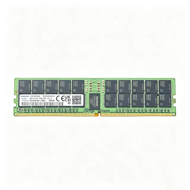
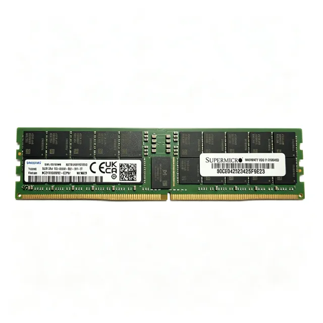
The Samsung M321RYGA0PB2-CCP is a 96 GB DDR5-6400 ECC Registered DIMM (RDIMM) server memory module rated at 6400 MT/s (PC5-51200) with 1.1 V nominal operation, organized as 2Rx4 (dual-rank, x4 DRAM) in a 288-pin RDIMM form factor. It is built from 40 FBGA 6Gx4 DDR5 DRAM devices and delivers a 72-bit ECC data path (12GX72 organization) for enterprise servers and workstations. A Registered DIMM (RDIMM) is a server memory module that places a register (RCD) and data buffers between the DRAM devices and the memory controller, reducing electrical load on the command/address bus and enabling higher module densities and higher speeds than unbuffered DIMMs. Within the memory hierarchy, an RDIMM sits above UDIMM and SODIMM in capacity and reliability, and below LRDIMM in load reduction; it is the mainstream choice for two-socket and four-socket x86 servers. DDR5 adds on-module PMIC power management, on-die ECC, and two 32-bit subchannels per module. Key features of the M321RYGA0PB2-CCP include 96 GB capacity in a single module, 6400 MT/s transfer rate, 2Rx4 organization for maximum rank-level interleaving, ECC Registered operation for data integrity, and 1.1 V DDR5 standard voltage. The 96 GB density is achieved with non-binary 24 Gb DDR5 DRAM dies, allowing high capacity without the cost of 3DS stacking. Technically, the module uses 40 FBGA 6Gx4 DRAM packages arranged in two ranks of twenty devices each, with a 288-pin edge connector and a 72-bit ECC data path. The on-module PMIC and SPD hub are part of the JEDEC DDR5 RDIMM architecture, and the module is 100% JEDEC compliant per distributor documentation. Typical applications include enterprise rack servers, virtualization hosts, in-memory databases, and high-performance workstations where 96 GB per DIMM enables dense configurations. The 2Rx4 organization and ECC RDIMM design suit memory-bandwidth-bound workloads such as AI inference, analytics, and VDI. When designing or upgrading, verify that the server platform supports 24 Gb non-binary DDR5 DRAM and 96 GB RDIMM densities, and populate DIMMs per the vendor's population rules to maintain rated 6400 MT/s speed. This page synthesizes distributor pricing, drop-in alternatives, and practical design notes not found in the manufacturer datasheet.

USD $3.445,31 En stock
M41T65Q6F - Serial RTC with Alarm, I2C, 1.3V-3.6V | STMicroelectronics
M41T65Q6F

M41T65Q6F - Serial RTC with Alarm, I2C, 1.3V-3.6V | STMicroelectronics

The STMicroelectronics M41T65Q6F is a serial access real-time clock (RTC) integrated circuit with alarm functions, providing a complete Clock/Calendar function plus 32.768 kHz output in a 16-pin VQFN exposed-pad package. The device communicates through a 400 kHz I2C (2-wire serial) interface, operates from 1.3 V to 3.6 V supply, and integrates memory-mapped registers for seconds, minutes, hours, day, date, month, year, and century tracking with automatic leap-year compensation through the year 2100. A Real-Time Clock (RTC) is a category of low-power timing IC that maintains accurate wall-clock time and date information independent of the system microcontroller. RTCs are essential components in any battery-backed system that must preserve time-of-day across power cycles. The M41T65 belongs to the RTC IC > Clock/Calendar > I2C RTC sub-family, and within ST's product hierarchy it sits under Timekeeping ICs > Serial RTC > RTC with Alarms. RTCs bridge the gap between digital logic and physical time by using a 32.768 kHz crystal oscillator as the time-base reference and counting oscillator cycles to derive seconds, minutes, hours, and calendar days. Key features of the M41T65Q6F include a wide operating voltage range of 1.3 V to 3.6 V (suitable for direct battery backup operation), integrated alarm and interrupt functions, a programmable square-wave output derived from the 32.768 kHz crystal, low power consumption typically below 1 microamp in battery backup mode, and an automatic backup switchover when VCC falls below a defined threshold. The 16-pin VQFN-EP (QFN-16) exposed-pad package provides low thermal resistance for stable operation across the -40 °C to +85 °C industrial temperature range and supports automated PCB assembly. Architecturally, the M41T65Q6F combines a 32.768 kHz crystal oscillator, frequency divider chain, BCD-coded time/date registers, I2C interface logic, alarm comparators, and a trickle charger circuit. The internal oscillator drives a divider that produces 1-second resolution. Time and date are stored in Binary-Coded Decimal (BCD) format for direct display compatibility. The integrated trickle charger allows the device to recharge an external backup supercapacitor or rechargeable battery when main power is present, then automatically switch over to backup supply on VCC failure. Typical applications include metering and data-logging systems, industrial controllers requiring time-stamped events, point-of-sale (POS) terminals, medical devices needing scheduled dosing or data recording, consumer electronics with calendar/alarm functions, and any battery-backed embedded system that needs to wake the host MCU at scheduled times. The low 1.3 V minimum supply also makes the M41T65Q6F well-suited for single-cell battery systems. When designing with the M41T65Q6F, ensure the 32.768 kHz crystal load capacitance matches the datasheet specification (typically 12.5 pF) and place the crystal traces as short and symmetric as possible to minimize parasitic capacitance. A decoupling capacitor of 0.1 microfarad should be placed within 2 mm of the VCC pin. The exposed pad (EP) must be soldered to the ground plane for mechanical and thermal reliability. This page synthesizes distributor pricing, package-equivalent alternatives in the same ST M41Txx RTC family, and practical design notes not aggregated on the manufacturer datasheet PDF.

Cotización Contacto