CI de interfaz
Subcategorías
Productos (1145)

PCA9600D,118 - 1 MHz I2C-bus Buffer/ReDriver | NXP | 8-SO
The NXP PCA9600D,118 is a dual bidirectional bus buffer/ReDriver designed to isolate I²C-bus capacitance in point-to-point and multipoint applications up to 4000 pF. Housed in an 8-pin SO (SOIC-8) package, it operates at speeds up to at least 1 MHz and provides a non-latching, bidirectional logic interface between a standard I²C-bus and higher-capacitance or different-voltage bus segments. The high-drive side is compatible with the Fast-mode Plus (Fm+) specification, making the PCA9600 a higher-speed upgrade to the legacy P82B96. What is an I²C bus buffer? An I²C-bus buffer/ReDriver is a dedicated interface IC that sits between two bus segments to overcome the 400 pF capacitive limit of standard I²C. By isolating capacitance, a buffer allows engineers to extend bus length, add more nodes, use lower-cost cabling, or bridge between logic-voltage domains. Buffers/ReDrivers belong to the interface IC hierarchy: interface IC > bus buffer > I²C extender > signal conditioning, and are widely used in industrial backplanes, sensor arrays, and LED lighting chains where long cable runs would otherwise exceed the bus's RC budget. Key features of the PCA9600 include an operating supply voltage range from 2.5 V to 15 V on the low-voltage (standard I²C) side, with logic-level translation capability through the dual-rail architecture. The part is specified for -40 °C to +85 °C operation and offers high-impedance logic pins that prevent bus latching during plug-in or brown-out events. The device is bus-isolating rather than bus-repeating, so it cannot sink the I²C pull-up current from both sides simultaneously—designers must provide pull-ups on each side. Architecturally, the PCA9600 uses an internal pass-FET-style transmission gate with direction-sense amplifiers that detect which side is driving and steer current accordingly without requiring an external direction-control pin. The result is a drop-in, transparent bus extender that does not occupy an I²C address and does not appear as a node. Compared to discrete MOSFET plus pull-up solutions, the PCA9600 guarantees matched thresholds, controlled rise/fall times, and known hot-swap behavior across temperature. Common applications include industrial control backplanes, large-display LED driver chains, remote sensor arrays, and any system where the I²C master sits on one PCB and the slaves are several meters away on a cable or harness. The PCA9600D,118 ships on 13-inch tape and reel and is fully RoHS compliant, targeting high-reliability commercial and industrial designs. When designing with this part, pay close attention to the pull-up placement: each bus segment requires its own pull-up resistor sized for that segment's capacitance and the target rise time. Designers commonly pair the PCA9600 with 4.7 kΩ pull-ups on the master side and 1 kΩ to 2.2 kΩ pull-ups on the high-drive side to handle the larger bus capacitance.
PCA9601D,118 - 1MHz Fm+ I2C Bus Buffer SO-8 | NXP
The NXP PCA9601D,118 is a dual bidirectional I2C-bus buffer and repeater supporting operation to at least 1 MHz (Fast-mode Plus), with a wide 2.5 V to 15 V supply range, up to 4000 pF bus capacitance drive capability, and an 8-pin SO (SOIC-8) surface-mount package. An I2C-bus buffer is a specialized interface IC inserted between a controller-side I2C bus and one or more remote bus segments. Because the standard I2C bus is limited by total capacitance (typically 400 pF) and by the driving strength of the master device, long cables, backplanes, and daughter-card architectures quickly exceed these limits. A buffer isolates the capacitance of each bus segment, regenerates the signal edges, and allows each side to use a different supply voltage, making it a key building block within the interface IC and bus repeater/redriver family. Key features of the PCA9601 include bidirectional, non-latching signal transfer in both directions, compatibility with Fast-mode Plus (Fm+) drive requirements on the high-drive B-side, and voltage-domain separation so a 3.3 V controller bus can drive a 5 V, 12 V, or 15 V remote bus. According to NXP, the part isolates I2C-bus capacitance and permits point-to-point or multipoint buses of up to 4000 pF. Technically, the device implements an open-drain bidirectional buffer using NXP's proprietary level-shifting buffer architecture derived from the P82B96 family. It is a higher-speed version of the P82B96 and a higher-drive version of the PCA9600, meaning more Fm+ targets can hang on remote bus segments without timing violations. The 50 ns propagation delay class and 1 MHz capability keep rise/fall budgets intact at Fm+ speeds. Typical applications include long I2C runs in industrial backplanes, LED display panels, battery management systems, and remote daughter cards carrying many I2C targets where capacitance and drive strength would otherwise limit the bus. Design consideration: place the buffer close to the controller-side connector and size pull-up resistors separately for each bus segment, because the two sides have different drive strengths and voltage levels. This page synthesizes distributor pricing, drop-in alternatives, and practical design notes not found in the manufacturer datasheet.

PCA9601DPZ - 1MHz Dual I2C-Bus Buffer | NXP Semiconductors
The NXP Semiconductors PCA9601DPZ is a dual bidirectional I2C-bus buffer and repeater that isolates bus capacitance and drives loads up to 4000 pF, operating at speeds up to 1 MHz (Fast-mode Plus) in an 8-pin TSSOP surface-mount package. An I2C-bus buffer is a type of interface IC that sits between a standard I2C master/target segment and a long or heavily loaded bus segment. In the interface IC hierarchy (bus buffer -> signal repeater -> interface IC), its role is to regenerate signal edges and isolate capacitance, because the I2C specification limits total bus capacitance and rising-edge time. By splitting one bus into short segments, a buffer allows long cables, backplanes, and daughter-card interconnects that would otherwise violate I2C timing. Key features of the PCA9601 include 4000 pF bus drive capability, non-latching bidirectional logic that preserves the wired-AND I2C arbitration and clock-stretching behavior, and a high-drive side compatible with Fast-mode Plus (Fm+) specifications. It supports level translation between mixed-voltage bus segments (3.3V, 5V, and higher-voltage buffered sides), enabling communication between 3.3V and 5V systems while maintaining signal integrity and timing. The PCA9601 is architecturally a higher-speed version of the well-established P82B96 and a higher-drive version of the PCA9600. Its buffered, non-latching topology means the buffer never locks up during arbitration or repeated starts, a common failure mode of simpler repeater designs. The high drive strength allows many more Fast-mode Plus targets on remote daughter cards than an unbuffered bus could support. Typical applications include point-to-point and multipoint extension of I2C buses across cables and backplanes, isolating capacitance of remote daughter cards, mixed-voltage (3.3V/5V) system interfacing, and industrial or telecom equipment where many Fm+ targets must share a long bus. Devices such as the PCA8574, PCA9539, and PCA9538 I/O expanders are typical loads at the far end of a buffered segment. Design considerations: the PCA9601 specifies an operating temperature range of 0 C to 85 C, so it is intended for commercial and industrial indoor use rather than automotive-grade environments. Verify bus segment capacitance on both sides and follow the datasheet for pull-up sizing on the buffered side to meet Fm+ rise-time requirements. This page synthesizes distributor pricing context, drop-in family alternatives, and practical design notes not found in the manufacturer datasheet, with data verified as of 2026-10-20.

PCA9614DP,118 - 2-Ch Fm+ Differential I2C Bus Buffer | NXP
The NXP PCA9614DP,118 is a 2-channel multipoint Fast-mode Plus (Fm+) differential I2C-bus buffer with 400 kHz buffered operation, dual-supply differential signaling, and a 10-pin TSSOP (DP) surface-mount package. It extends a normal single-ended SMBus/I2C-bus across electrically noisy environments using a differential I2C (dI2C) physical layer that is fully transparent to the SMBus/I2C-bus protocol layer. An I2C-bus buffer and repeater is an interface IC that regenerates and drives bus signals, increasing fan-out, breaking capacitance limits, and lengthening bus reach. Within the interface IC hierarchy, buffer ICs sit between an I2C master/peripheral and the physical wire, and differential buffers such as this one add a robust physical layer without changing the protocol, so standard controllers require no firmware changes. Key features include two independent buffer channels supporting multipoint dI2C links over long cables, an EN pin that places the device in an idle state to stop traffic propagation, and an internal pull-up on EN that holds the device enabled by default. The differential transmission rejects common-mode noise, making the link tolerant of ground potential differences between boards. Technically, the PCA9614 converts the single-ended SDA/SCL levels into a differential pair per channel at the buffer output side, and converts back to single-ended at the receiving end when paired with another differential buffer. Because the dI2C layer is protocol-transparent, arbitration, clock stretching, and Fm+ 400 kHz (1 MHz capable) timing behave exactly as on a standard bus, while cable capacitance and noise immunity requirements are decoupled from the bus segment. Typical applications include industrial automation bus extension, rack and backplane inter-board communication in servers, battery management systems in electrically noisy traction environments, and long-run I2C links between enclosures or display modules. A key design consideration is power sequencing of the dual supplies (VDD(A) on the single-ended side and VDD(B)/VL on the differential side); both must remain within the datasheet recommended operating conditions and EN should be held low during startup to prevent glitching. This page synthesizes distributor pricing, drop-in alternatives, and practical design notes not found in the manufacturer datasheet, with freshness data as of 2026-10-20.
PCA9615DPZ - 2-Ch I2C Fast-Mode Plus Diff Buffer | NXP
The NXP Semiconductors PCA9615DPZ is a 2-channel multipoint Fast-mode Plus differential I2C-bus buffer with hot-swap logic, operating up to 1 MHz, housed in a 10-pin TSSOP (SOT552-1) package. It supports standard I2C, Fast-mode, and SMBus compatibility, with single-ended I2C on the card side up to 540 pF and differential I2C on the cable side supporting multi-drop bus up to 3 meters. The device uses an external DCEN pin to enable/disable the differential driver and operates from dual supplies, typically VDD(A) on the single-ended side and VDD(B) on the differential side. A signal buffer, repeater, or redriver is an active interface IC placed in-line on a bus to restore signal integrity when the load capacitance or physical distance exceeds the limit of the bus specification. In the I2C hierarchy, this part is a specialized bus extender/repeater that converts a single-ended SDA/SCL pair into a differential pair for transmission over twisted-pair or shielded cable, then converts back at the far end. This is essential in industrial control, automotive sensor backbones, and large backplane systems where standard I2C's capacitive limit (~400 pF) is insufficient. Key features of the PCA9615DPZ include differential transmission across a cable up to 3 meters at Fast-mode Plus speeds, hot-swap logic that allows the card to be inserted into a live backplane without disturbing the bus, wide supply range (2.7 V to 5.5 V on VDD(A) and 3.0 V to 5.5 V on VDD(B)), and AEC-Q100 qualification for automotive applications. The hot-swap circuitry prevents inrush current and bus glitches during card insertion. The differential pair uses low-voltage signaling to reduce EMI compared to single-ended transmission. Typical applications include industrial I2C backplane extension, automotive sensor networks, hot-swappable I/O cards, multi-drop I2C sensor clusters, and remote sensor/PCI configuration. The device is particularly valuable where cables must span meters between cards, sensors, or backplane slots, and where live insertion is needed without disrupting the system bus. When designing with this part, ensure both VDD rails are decoupled with 100 nF ceramic capacitors placed within 5 mm of the supply pins. Verify the differential pair routing on the cable side is twisted-pair or shielded to meet EMI requirements; the part itself does not include cable termination resistors, so external 100 ohm differential termination may be required at the far end for very long runs.

PCA9616PW - 3-Channel Differential I2C Bus Buffer | NXP
The NXP Semiconductors PCA9616PW is a dual-supply, 3-channel multipoint Fast-mode Plus (Fm+) differential I2C-bus buffer with hot-swap logic, packaged in a 16-pin TSSOP (PW) surface-mount package. It buffers the single-ended SMBus/I2C-bus up to 1 MHz and converts it to a differential I2C (dI2C) bus that reliably extends communication through electrically noisy environments over cable runs of at least 3 meters, or longer at reduced clock speeds. A differential I2C-bus buffer, sometimes called a bus repeater or redriver, is an interface IC that belongs to the signal buffer family within the broader hierarchy of interface integrated circuits. Where a plain I2C bus uses open-drain single-ended lines vulnerable to ground bounce and common-mode noise, a dI2C buffer translates the bus into a differential current-mode signaling scheme, dramatically improving common-mode noise immunity while remaining fully compatible with existing Standard-mode, Fast-mode, and Fast-mode Plus I2C and SMBus devices. Key features of the PCA9616PW include its 3-channel multipoint architecture, which supports a dI2C bus shared by multiple nodes for multipoint topologies; its dual-supply design isolating the single-ended side from the differential side; support for Fast-mode Plus operation at 1 MHz; and integrated hot-swap logic that allows a card or module to be inserted into or removed from a live backplane without corrupting bus transactions. Signal direction is fully automatic, requiring no external direction-control signal. Technically, the device pairs each single-ended SDA and SCL line with differential transmit/receive pairs on the cable side, using current-mode differential drivers and receivers with high common-mode noise rejection. Because it is a multipoint buffer, several PCA9616 devices can share one differential cable, enabling distributed systems such as rack-mounted cards, industrial backplanes, and remote sensor clusters. NXP documents cable extension of at least 3 m, with longer runs achievable at lower bus speeds. Typical applications include industrial backplane I2C distribution, telecom and server shelf management, multipoint sensor networks in electrically noisy factory environments, and hot-pluggable module bus extension. The hot-swap logic makes it especially suitable for field-replaceable cards. Design consideration: plan the differential bus topology to respect multipoint stub-length limits, and verify supply sequencing on both the single-ended and differential rails against the manufacturer datasheet to guarantee correct hot-swap behavior. This page synthesizes distributor pricing, drop-in replacement analysis, and practical design notes not found in the manufacturer datasheet.

PCA9670BS,118 - 8-bit Fm+ I2C I/O Expander w/ Reset, HVQFN-16
The NXP PCA9670BS,118 is a remote 8-bit I/O expander for Fast-mode Plus (Fm+) I2C-bus with reset, packaged in a 16-pin HVQFN (3x3 mm) with exposed thermal pad. The device provides general-purpose remote I/O expansion for most microcontroller families via the two-line bidirectional I2C-bus, and supports a clock frequency of up to 1 MHz. Operating supply range is 2.3 V to 5.5 V, allowing use with 3.3 V and 5 V logic rails. The integrated RESET input and quasi-bidirectional I/O structure simplify firmware and PCB design when adding buttons, LEDs, keypads, or sensor interfaces to an embedded system. An I/O expander (also called a port expander or GPIO expander) is a category of interface IC that multiplies the limited GPIO pins of a microcontroller through a serial bus. In the taxonomy I/O expander -> interface IC -> integrated circuit -> semiconductor, the PCA9670BS sits in the parallel-bus-expansion tier and uses I2C as the transport. By attaching the part to SCL/SDA, designers gain eight additional quasi-bidirectional I/O pins addressed through a 7-bit slave address. Three hardware address pins (A0, A1, A2) allow up to 64 PCA9670 devices on the same bus, supporting up to 512 I/Os (for example 512 LEDs) without external bus buffers. Key features include 1 MHz Fm+ bus support (compared with 400 kHz for the classic PCF8574), a hardware RESET pin that reverts all ports to inputs, low standby current, and 5 V tolerant I/O structure that tolerates bus pulls above VDD. The HVQFN-16 (3x3) package provides a low 0.5 mm profile with an exposed die attach paddle for improved thermal performance, making it suitable for compact industrial, consumer, and IoT designs. NXP specifies ESD protection exceeding 2 kV HBM on the I/O pins, and the part is qualified to the industrial -40 C to +85 C operating range. The PCA9670 architecture uses an I2C state machine with interrupt logic for input-change notifications and a separate RESET input that asynchronously clears internal state. Internally each I/O pin is a quasi-bidirectional structure - capable of sinking current to drive LEDs directly while also serving as an input when written high. This dual-mode behavior differs from push-pull GPIO and is important when migrating designs from the older PCF8574/PCF8575 family. Typical applications include keypad and button-matrix scanning in white goods and access control, LED driving and chase patterns in industrial control panels, sensor multiplexing on Raspberry-Pi-class SBCs where the host lacks enough native GPIO, and general-purpose I/O expansion in PLC and HVAC controllers. The wide 2.3-5.5 V supply range plus 1 MHz Fm+ bus speed also suits battery-powered IoT nodes that need to minimize I2C transaction time. When designing with this part, place 100 nF decoupling close to VDD, use external pull-ups on SDA/SCL sized for the bus capacitance (typically 4.7 kohm at 1 MHz), and avoid leaving the RESET pin floating - tie it to VDD through a 10 kohm resistor or drive it from the host MCU. The I/O sink capability must be checked against LED forward current; sourcing current is limited and the quasi-bidirectional behavior must be considered when interfacing to logic-level peripherals. This page synthesizes distributor pricing, drop-in alternatives, and practical design notes not found in the NXP datasheet.

PCA9675PW,118 - 16-bit Fm+ I2C I/O Expander | NXP | TSSOP-24
The NXP PCA9675PW,118 is a 16-bit remote I/O expander for the Fast-mode Plus (Fm+) I²C-bus, supplied in a 24-pin TSSOP (PW) package and shipped on 13-inch tape and reel. It operates from a supply voltage of 2.3 V to 5.5 V, clocks the I²C interface at up to 1 MHz, and exposes 16 quasi-bidirectional I/O lines that can source/sink up to 30 mA per pin with a 100 mA total package limit. An I/O expander (also called a port expander or GPIO expander) is a category of interface IC that increases the number of general-purpose I/O pins available to a host microcontroller over a serial bus such as I²C. In the system hierarchy it sits between the MCU and the discrete digital loads (LEDs, keypads, sensors, relay coils), translating compact I²C transactions into parallel pin-level updates. The PCA9675 belongs to NXP's Fm+ family, which is optimized for high-speed serial I/O expansion in noisy or long-trace industrial backplanes. Key features include three hardware address pins (A0/A1/A2) supporting up to eight PCA9675 devices on the same bus, an active-low interrupt output (INT) that asserts when any input changes and releases on the next I²C read, an active-low reset input with internal power-on reset, and per-pin latch-up current exceeding the 100 mA JESD78 limit. The device is a drop-in upgrade for the legacy PCF8575, lifting bus speed from 400 kHz to 1 MHz and raising sink current capability. Typical applications include PWM dimming of LED arrays (each pin can be modulated at >1 MHz bus rates), keypad and switch-matrix scanning, fan-speed and relay control in industrial PLCs, and general-purpose I/O expansion for low-pin-count MCUs in white goods, HVAC, and IoT edge nodes. Designers value the wide 2.3–5.5 V supply range because it allows direct interface to both 3.3 V and 5 V microcontrollers without level shifters. When designing with this device, place 100 nF decoupling on VDD as close as possible to the pin and pull SDA/SCL high with 4.7 kΩ resistors for standard 400 kHz operation or 1 kΩ for the full 1 MHz Fm+ rate. Note that quasi-bidirectional outputs require no external pull-up on the load side because an internal weak pull-up is enabled after each read cycle.
PCA9703PW/Q900 - 16-bit SPI GPI, 18V Tolerant | NXP
The NXP Semiconductors PCA9703PW/Q900,118 is an 18 V tolerant, 16-bit SPI General Purpose Input (GPI) shift register with maskable interrupt output, housed in a 24-pin TSSOP (PW) package rated -40 C to +125 C. It operates as an SPI slave at up to 5 MHz and monitors 16 switch or logic inputs with 18 V input tolerance, making it a low-power solution for high-voltage switch status monitoring in automotive and industrial systems. A GPI (General Purpose Input) shift register is a type of input-only I/O expander within the broader hierarchy of interface ICs -> I/O expanders -> parallel-in serial-out shift registers. Unlike I2C GPIO expanders, SPI GPI shift registers stream input states to a microcontroller as a serial bit field, which minimizes pin count on the host MCU and gives deterministic, fast read-back of many switch contacts. Key features include 16 input-only channels tolerant to 18 V regardless of the device supply, a maskable INT output that flags any change of input state, a 3 V input switching threshold for robust noise immunity, and SPI compatibility up to 5 MHz. The Q900 suffix and /Q900,118 ordering code identify the automotive AEC-Q100 compliant variant with extended -40 C to +125 C operation; NXP states that PCA9703PW/Q900 is AEC-Q100 compliant and PPAP documentation is available via i2c.support@nxp.com. Technically, the PCA9703 samples its 16 GPI inputs into an internal shift register and shifts data out on MISO under host control of CS and SPI clock. Any input change (open, closed, or 12 V/24 V level via divider) triggers the interrupt output, which can be masked to prevent nuisance CPU wake-ups. The low-power CMOS process keeps static consumption minimal, which is critical for always-on battery-backed switch monitoring. Typical applications include automotive switch monitoring (door, window, seat, and steering-column switches), industrial control panels and limit-switch monitoring, and 12 V/24 V system status sensing where contacts ride on battery-level rails the chip inputs directly tolerate. A key design consideration is input threshold scaling: although inputs tolerate 18 V, the 3 V threshold means designers must confirm logic levels and switch pull-up arrangements so that a valid LOW is below threshold and a valid HIGH is safely above it across temperature. This page synthesizes distributor pricing, lifecycle status, drop-in alternative analysis, and practical design notes not found in the manufacturer datasheet alone.
PCA9703PW/Q900,118 - 16-Bit SPI GPI 18V Tolerant | NXP
The NXP Semiconductors PCA9703PW/Q900,118 is an 18 V tolerant SPI 16-bit General Purpose Input (GPI) shift register with maskable interrupt output, supplied in a 24-pin TSSOP package rated for -40 C to +125 C automotive operation with a 4.5 V to 5.5 V supply and a 5 MHz SPI clock. A general purpose input shift register is a specialized interface IC that converts parallel logic levels from switches or sensors into a serial data stream. In the system hierarchy it sits between raw switch inputs and a microcontroller: instead of dedicating 16 MCU pins to switch monitoring, a single SPI port reads all 16 inputs as a serial word, reducing pin count, wiring harness complexity, and cost in distributed control systems. Key features include 18 V tolerance on all GPI pins, allowing direct connection to automotive battery-nominal rails without level shifting; a maskable interrupt output (INT) with an INT_EN pin that disables the inputs and interrupt to minimize battery drain in cyclically powered systems; and an SDIN pin with pull-down that supports daisy-chaining multiple devices on a single SPI bus for 32, 48, or more inputs. Architecturally, the PCA9703 uses a shift register with a dedicated output enable controlled by CS. The 3 V logic thresholds on the serial interface ensure compatibility with both 3.3 V and 5 V controllers. Switch status is captured in the parallel input register and shifted out MSB-first on SCLK edges, with the interrupt flag readable on the first serial byte so the MCU can branch quickly on any input change. Typical applications include automotive switch monitoring for door, seat, and steering-column controls, body control modules and keypads, and industrial panels requiring isolated or battery-tolerant digital inputs. The 18 V tolerance is the decisive parameter wherever switches are wired to unregulated supply rails. A key design consideration: the GPI inputs require external pull-up or pull-down resistors to the switched rail; the INT_EN pin should be driven low during system sleep to eliminate quiescent current drawn through those resistors. This page synthesizes distributor pricing, drop-in alternative analysis, design notes, and application guidance not found in the manufacturer datasheet, making it a one-stop engineering reference for the PCA9703PW/Q900,118.
PCA9704PW/Q900 - 8-bit SPI GPI 18V Tolerant | NXP
The NXP Semiconductors PCA9704PW/Q900 is an 8-bit, 18 V tolerant SPI General Purpose Input (GPI) shift register with maskable interrupt, AEC-Q100 qualified for automotive applications, housed in a 16-pin TSSOP (PW) package. It monitors the status of switch inputs and reads them out over a standard SPI interface running at up to 5 MHz. A general-purpose input expander is an interface IC that offloads switch or status-signal monitoring from a microcontroller. In the signal-chain hierarchy, the PCA9704 sits between discrete switch contacts and an MCU's SPI peripheral: GPIO expander -> interface IC -> mixed-signal logic device. Input expanders are used when an MCU lacks sufficient input pins or when switch signals sit at voltages higher than the MCU supply, as is common in automotive 12 V and 24 V electrical systems. Key features include eight input channels each tolerant to 18 V, allowing direct connection to battery-referenced switch contacts without external level shifting or clamping networks. The SPI interface supports read-out at up to 5 MHz, and a maskable interrupt output (INT) alerts the host controller only when inputs change, enabling low-power polled or event-driven system architectures. Technically, the PCA9704 is implemented as a parallel-in serial-out shift register with input latching. When the host asserts the chip-select, the current input state is latched and shifted out on the SPI data line; devices can be cascaded to expand beyond eight inputs on a single SPI bus. The /Q900 suffix denotes NXP's automotive product-line extension with AEC-Q100 compliance and PPAP support, distinguishing it from the commercial-grade PCA9704PW. Typical applications include automotive switch monitoring (door, seat, and key contacts), industrial control-panel status readback, and system diagnostics where battery-level fault or presence signals must be safely captured by a low-voltage controller. Design consideration: although the 18 V tolerance removes the need for input dividers, verify worst-case battery load-dump transients in automotive systems and confirm that the interrupt mask register is initialized before enabling INT to avoid spurious wake-ups at power-up. This page synthesizes distributor data, automotive-grade alternative options, and practical SPI integration notes not found in the manufacturer datasheet, with pricing verified as of 2026-10-19.
PCAL6408AHK - 8-Bit I2C I/O Expander, XQFN-16 | NXP
The NXP Semiconductors PCAL6408AHK is a low-voltage translating, 8-bit general-purpose I/O expander with interrupt output, reset, and Agile I/O configuration registers, interfacing to a host microcontroller via I2C-bus/SMBus at up to 400 kHz in a 16-pin XQFN (1.8 x 2.6 mm) package. An I/O expander is a peripheral IC that adds extra general-purpose input/output pins to a microcontroller or embedded processor over a serial bus such as I2C or SMBus. In the system hierarchy, it sits within the interface IC family, under mixed-signal peripheral devices, and complements microcontrollers whose native GPIO count is exhausted. Expanders offload GPIO expansion while consuming only two bus wires (SDA, SCL), conserving processor pins and board routing. Key features include a wide supply range of 1.65 V to 5.5 V, dual power rails for true voltage level translation between logic domains, programmable output drive strength, and latchable inputs. The interrupt output and active-low reset provide robust event-driven and fault-recovery behavior in multi-slave I2C systems. The Agile I/O feature set - configurable output drive, input latch, and pull-up/pull-down enable - allows system designers to tune signal integrity and power per pin, which is significant in mixed-voltage designs where a 1.8 V MCU must safely drive 3.3 V or 5 V peripherals. Open-drain and push-pull operating modes over I2C/SMBus at 400 kHz provide flexible bus integration. Typical applications include GPIO expansion in portable and battery-powered devices, level translation between low-voltage processors and legacy 5 V peripherals, sensor and keypad scanning, LED control, and backplane status monitoring in industrial systems. Design consideration: because the XQFN-16 package measures only 1.8 x 2.6 mm, the exposed pad must be soldered to a grounded PCB land pattern for reliable thermal and mechanical performance; verify land-pattern tolerances before assembly. This page synthesizes distributor pricing context, drop-in alternatives, practical design notes, and AEO-optimized FAQs not found in the NXP datasheet.

PCF85176T/1 - 40x4 LCD Segment Driver I2C TSSOP-56 | NXP
The NXP Semiconductors PCF85176T/1 is a universal LCD segment driver with 40 segments and 4 backplanes, packaged in a 56-pin TSSOP (TSSOP-56). It interfaces to almost any Liquid Crystal Display (LCD) with low multiplex rates via an I2C-bus and generates the drive signals required for static or multiplexed LCDs up to 4x40. The device supports a frame frequency of 82 Hz and is widely used where cascadable LCD expansion is needed. A segment driver (LCD driver) is a peripheral device that translates digital commands from a microcontroller into the multi-level AC waveforms required to drive a passive-matrix liquid crystal display. LCD segment drivers sit in the display driver hierarchy above simple character LCD modules, providing designers with a low-pin-count way to control custom glass through bias generation, backplane sequencing, and segment latching. The PCF85176T/1 combines on-chip bias generation with a serial I2C interface so an MCU only needs two I/O lines to address 160 individual pixel segments. Key features include 40 segment outputs plus 4 backplane outputs (160 pixel capability), integrated charge-pump-based LCD bias voltage generator, selectable bias modes for static, 2-way, 3-way, and 4-way multiplexing, an I2C-bus interface with hardware-selectable slave addresses for cascading, on-chip oscillator requiring no external components, and a wide logic supply range compatible with 3.3 V and 5 V microcontrollers. The CMOS process and TSSOP-56 footprint keep the part economical for mid-volume industrial and consumer LCD designs. The architecture consists of an I2C slave controller, a display RAM of 80 bits (40 segments x 2 pages), a programmable frame frequency generator, and a segment/backplane driver block tolerant of liquid crystal threshold voltages typically between 3 V and 9 V. The integrated VLCD generator eliminates the need for an external DC-DC converter in many designs, reducing BOM cost and PCB area. Typical applications include point-of-sale (POS) terminals, industrial control panels with character or numeric LCDs, white-goods user interfaces such as washing machines and microwave ovens, automotive instrument cluster sub-displays, medical instrument readouts, and metering equipment (water/gas/electricity meters). Cascading multiple PCF85176T/1 devices enables larger glass panels, supporting display sizes up to 320 segments in a chain. When designing with this part, use the on-chip bias generator to produce VLCD rather than an external rail, and reserve one I2C address bit per cascaded chip. Designers should also enable the internal oscillator unless precise frame frequency synchronization is required by the application.

PCF8562TT/2 - 4x32 I2C LCD Segment Driver | NXP | TSSOP-48
The NXP PCF8562TT/2 is a universal LCD segment driver with 4 backplanes and 32 segments, controlled via the two-line bidirectional I2C-bus, housed in a 48-pin TSSOP (SOT362-1) package. It supports supply voltages of 2.5V, 3.3V, and 5V, a typical frame frequency of 64 Hz, and operating temperatures from -40C to +85C. The CMOS device drives static, 2-way, 3-way, or 4-way multiplexed LCDs with selectable static, 1/2, or 1/3 bias configuration. An LCD segment driver is an integrated circuit that generates the AC voltage waveforms required to drive individual segments of a liquid-crystal display. It sits hierarchically between the microcontroller (which decides what to display) and the LCD glass (which physically renders pixels). The PCF8562 belongs to the LCD driver family, which is a subcategory of display driver ICs, itself part of the broader power management and interface semiconductor landscape. Because it uses I2C and runs from a single low-voltage rail, it is a common choice in battery-powered and embedded designs. Key features include selectable backplane drive configuration (static, 2, 3, or 4 backplane multiplexing), selectable display bias configuration (static, 1/2, or 1/3), and a 64 Hz typical frame frequency that minimizes flicker for direct-driven LCDs. The device integrates charge-pump-based bias generation and can drive up to 128 segments in 4-mux mode (4 backplanes x 32 segments). Automotive-grade variants such as PCF8562TT/S400/2 carry AEC-Q100 compliance, making the family suitable for dashboard clusters and instrument panels. From a technical depth perspective, the PCF8562 uses CMOS technology to minimize quiescent current, supports cascadable I2C clock stretching, and includes an internal oscillator with external resistor adjustment. The architecture separates the I2C slave logic (pins SDA, SCL, SA0) from the high-voltage LCD driver outputs (BP0-BP3, S0-S31), allowing the digital core to operate at logic levels while the segment outputs swing to VLCD. Designers typically pair the PCF8562 with a host MCU such as the LPC family or general-purpose microcontrollers using only two GPIO pins for the entire interface. Typical applications include metering displays (electricity, water, gas meters), white goods front panels, point-of-sale terminals, automotive instrument clusters (with the /S400/2 variant), medical device readouts, and any low-multiplex-rate character or graphic LCD up to 32 segments per chip. Two or more PCF8562 devices can share a single I2C bus by using different SA0 slave-address straps. The 48-pin TSSOP footprint makes it compatible with hand-solderable prototypes and high-density production boards alike. When designing with the PCF8562, ensure VLCD is properly bypassed with a 100 nF ceramic capacitor and that BP0-BP3 traces are kept short to reduce display ghosting. Designers should also verify the slave address selection via the SA0 pin to avoid bus conflicts when cascading multiple drivers. This page synthesizes distributor pricing, drop-in alternatives, and practical design notes not found in the manufacturer datasheet alone.

PCF8574AT/3,518 - 8-bit I2C I/O Expander | NXP SOIC-16
The NXP PCF8574AT/3,518 is an 8-bit I/O expander with quasi-bidirectional I/O pins, an I2C-bus interface operating up to 100 kHz, and an open-drain interrupt output, housed in a 16-pin SO (SOIC-16, MS-013/SOT-162-1) plastic package. It operates from 2.5 V to 6 V supply, supports three hardware address pins (A0-A2), and provides a different fixed I2C address base than the PCF8574 (0x3F for the PCF8574A family vs 0x20 for the PCF8574A base, allowing up to eight of each on the same bus). The CMOS silicon-gate design draws low quiescent current (typ. 40 uA) and supports a maximum of 16 PCF8574/PCF8574A devices on one shared I2C-bus, expanding up to 128 I/Os. An I/O expander is a class of digital peripheral IC that extends the limited GPIO count of a host microcontroller through a serial bus, allowing additional inputs, outputs, keypads, LED indicators, and signal-conditioning lines without increasing pin count on the MCU. Within the hierarchy of interface ICs (also called bus expanders or GPIO extenders), the PCF8574AT belongs to the I2C-bus parallel-port family, positioned between simple shift-register expanders (which lack interrupt capability) and full SPI/I2C port-mapped devices. This category sits under digital logic and interface ICs in broader semiconductor taxonomy, supporting both consumer and industrial designs where MCU pin count is constrained. Key features include quasi-bidirectional I/O that can directly drive LEDs without external pull-ups (sinking capability of up to 25 mA per pin, max 100 mA total), an active-low interrupt output (INT) that signals the host when any input state changes, and 400 kHz Fast-mode I2C capability on the PCF8574A/PCF8574AT family variants. The device integrates a noise filter on the SCL/SDA lines and supports clock stretching as a slave device. The PCF8574AT uses a CMOS silicon-gate architecture with latched output registers and input latches on every I/O pin. The quasi-bidirectional design uses a weak pull-up (typically 100 uA current source) to drive outputs high; pulling low requires the pin to actively sink current. This architecture eliminates the need for external pull-up resistors on outputs while maintaining low standby current. Typical applications include driving LED arrays, LCD segment interfaces, keypad matrix scanning, fan-speed monitoring, relay control boards, and general-purpose I2C slave peripheral expansion in industrial control, consumer electronics, and embedded systems. Engineers commonly pair the PCF8574AT with low-power MCUs (such as the LPC1100 or PIC16F families) to add 8-bit digital I/O over only two signal wires. When designing with this part, note that the quasi-bidirectional I/O pins have an asymmetric drive capability - they source weakly (100 uA) but sink strongly (25 mA per pin). This makes them ideal for LED-driving (sink mode) but less suitable as push-pull signal drivers. Always respect the absolute maximum of 100 mA total current through the VDD/GND pins to avoid latch-up. This page synthesizes distributor pricing, drop-in same-package alternatives, and practical design notes not found in the manufacturer datasheet alone, including cross-references for the very similar PCF8574T/3 (different I2C address range).

PCF8574PWR - 8-bit I2C I/O Expander 20-TSSOP | Texas Instruments
The Texas Instruments PCF8574PWR is a remote 8-bit I/O expander for the I2C bus, designed for 2.5 V to 6 V VCC operation, packaged in a 20-pin TSSOP (PW) with Tape and Reel packaging. It provides general-purpose remote I/O expansion for most microcontroller families via the I2C interface (serial clock SCL, serial data SDA) and supports an interrupt (INT) output to flag input changes to the host. An I/O expander is a type of interface IC that sits between a host controller (typically a microcontroller with limited GPIO) and external peripherals, translating a serial bus into multiple parallel digital lines. The PCF8574 belongs to the I2C I/O expander family -> interface IC -> integrated circuit -> semiconductor. By cascading multiple devices, designers can scale I/O count without redesigning the host board, making I/O expanders essential in space-constrained and pin-limited embedded designs. Key features include 8 quasi-bidirectional I/O pins, 100 kHz I2C clock rate, three hardware address pins (A0-A2) allowing up to 8 devices on the same bus (16 combined with PCF8574A), an active-low interrupt output that wakes the host on input changes, and low standby current of 2.5 uA typical. The PCF8574 uses the I2C address base 0x20 (PCF8574A uses 0x38), supporting up to 16 devices on a single bus for 128 I/Os. The quasi-bidirectional I/O architecture eliminates the need for a direction control register by using a clever pull-up/pull-down scheme, simplifying firmware. Each I/O can source 25 mA (LED drive capability) and sink up to 25 mA, sufficient to drive LEDs, keypads, or relay coils directly without buffering. Typical applications include keypad scanning for human-machine interfaces, LED driving for status indicators and display backlights, GPIO expansion for Raspberry Pi or ESP32-based projects, and industrial control panels. The wide 2.5 V to 6 V VCC range allows interfacing with both 3.3 V and 5 V logic without level shifters. When designing with this device, note that quasi-bidirectional I/Os are weak when transitioning to high - add an external pull-up resistor (typically 10 kohm) if driving heavy capacitive loads. The INT pin must be acknowledged by the host to clear the interrupt condition. This page synthesizes distributor pricing, drop-in alternatives, and practical design notes not found in the manufacturer datasheet alone.
PCF8574T - 8-bit I2C I/O Expander, SOIC-16 | NXP Semiconductors
The NXP Semiconductors PCF8574T is a remote 8-bit CMOS I/O expander for the two-line bidirectional I2C-bus, supporting 2.5V to 6V VCC operation and providing general-purpose remote I/O expansion for most microcontroller families. The PCF8574T integrates a quasi-bidirectional 8-bit parallel I/O port (P0-P7), an I2C-bus interface, and a hardware interrupt output (INT) that signals the host controller when input state changes, all in a 16-pin SOIC surface-mount package. What is an I/O expander? An I/O expander is an integrated circuit that adds additional general-purpose input/output pins to a microcontroller through a serial bus (typically I2C or SPI). It sits in the hierarchy: GPIO extender -> I/O expander -> interface IC -> digital semiconductor. The PCF8574T specifically uses a quasi-bidirectional I/O architecture that eliminates the need for a direction control register - each pin can be used as either input or output without explicit mode configuration. Key features of the PCF8574T include three hardware address pins (A0-A2) that allow up to 8 PCF8574T devices to share the same I2C-bus (selectable I2C addresses 0x20-0x27). The quasi-bidirectional I/O architecture requires no direction register, simplifying software drivers. The open-drain interrupt output (INT) is asserted when any input changes, enabling efficient event-driven polling. The device operates across 2.5V-6V VCC, supports I2C standard-mode (100 kHz) and fast-mode (400 kHz), and consumes very low standby current. The PCF8574T uses a silicon CMOS process with an open-drain interrupt line and open-drain bidirectional I/O pins. The quasi-bidirectional architecture drives a weak pull-up (current source) when outputs are HIGH and a strong pull-down when LOW, allowing the same pin to be read back without changing direction. The I2C slave address is programmed via A0, A1, A2; slave base address is 0x20 for PCF8574 and 0x38 for PCF8574A - this distinction is critical when selecting between variants. Typical applications include keypad scanning on human-machine interfaces (HMIs), LED driving on display panels and indicator boards, LCD bias generation, sensor monitoring via additional GPIOs, and adding GPIOs to small microcontrollers. The 0x20-0x27 address range also makes it ideal for multi-bus I/O expansion where multiple expanders must coexist. When designing with the PCF8574T, add 100 kohm pull-up resistors on SDA and SCL because the PCF8574T uses open-drain drivers (no internal pull-ups). Note that the "T" suffix denotes the SOIC-16 package, while "N" denotes DIP-16 and "BS" denotes SSOP-16 - same silicon die, different packages. The PCF8574 (base address 0x20) and PCF8574A (base address 0x38) are NOT drop-in replaceable without changing the host firmware address. This page consolidates distributor pricing, parametric equivalents (TI PCA9534, PCA9554, PCA9557), drop-in alternatives in the SOIC-16 footprint, and practical design notes not found in the manufacturer datasheet.
PCF8574TD - 8-bit I2C I/O Expander, SO-16 | NXP Semiconductors
The NXP PCF8574TD is a remote 8-bit I/O expander for the I2C-bus, supplied in a 16-pin SO (Small Outline) package with a -40C to +85C industrial temperature grade. The device operates from 2.5 V to 6 V VCC and provides eight quasi-bidirectional input/output pins that can be independently assigned as inputs or outputs, all controlled through the standard two-wire I2C interface. An I2C I/O expander is a type of interface IC that sits between a microcontroller and peripheral signals, translating serial commands from the I2C bus into parallel GPIO operations. The PCF8574 belongs to the I/O expander sub-category of interface ICs, itself part of the broader power management and inter-chip communication hierarchy. By adding eight extra quasi-bidirectional ports over only two wires, the PCF8574 lets small microcontrollers control keypads, LCDs, LEDs, and relays without sacrificing native pins for other functions. Key features of the PCF8574TD include a maximum standby current of 10 uA, an open-drain interrupt output (INT) that signals the host when an input changes state, and three hardware address pins (A0-A2) that allow up to eight PCF8574 devices on the same I2C bus (64 I/O lines). The quasi-bidirectional I/O architecture requires no direction-control register: a pin set HIGH is weakly pulled up (~100 uA source), and a pin set LOW is strongly pulled down, simplifying firmware and PCB layout. The PCF8574 uses a fixed I2C slave address of 0x20-0x27 (set by A2:A0), which distinguishes it from the PCF8574A variant (address range 0x38-0x3F). Both share the same SO-16 footprint, enabling dual-sourcing designs. The silicon CMOS process keeps quiescent current low enough for battery-backed applications. Typical applications include keypad scanning, LED driving arrays, LCD module backpacks, relay/Opto-coupler interfacing, and general-purpose GPIO expansion on 8051, ARM Cortex-M, ESP32, PIC, AVR, and MSP430 microcontrollers. The interrupt pin eliminates polling overhead in button or switch-matrix designs. When designing with this device, place a 0.1 uF decoupling capacitor close to VCC and 100 kohm pull-up resistors on SDA, SCL, and INT. Verify your firmware does not read the input port during the I2C ACK bit, as a transient high-current condition can occur on the quasi-bidi pins. This page synthesizes distributor pricing, drop-in alternatives (same-brand NXP variants and cross-brand TI equivalents), and practical design notes that complement, rather than duplicate, the manufacturer datasheet.

PCI4451GJG - Integrated PC Card & 1394 OHCI Controller | TI
The Texas Instruments PCI4451GJG is an integrated PC Card controller and 1394 (FireWire) OHCI controller that combines dual-slot CardBus (PCMCIA) support with a single 400 Mbps IEEE 1394a link in a single PCI device. It supports two independent PC Card slots compliant with the 1997 PC Card Standard, provides a 32-bit CardBus bridge for both slots, and integrates a 3.3 V physical layer for IEEE 1394 with one fully compliant cable port at 100/200/400 Mbps. The device is offered in a 257-ball MicroStar BGA (GJG) package, 16x16 mm, designed for space-constrained add-in cards and embedded platforms. Key features include PCI 2.2 host-side compliance, integrated 1394 OHCI 1.1 controller with cable power management, support for Zoom Video (ZV) port, ACPI 1.0 compliant power management with D0/D1/D2/D3 states and PME#, and programmable CardBus signal voltage (3.3 V / 5 V / VPP). The integrated PHY removes the need for an external 1394 link-layer chip, reducing both BOM count and PCB area versus two-chip implementations. Technically, the PCI4451 uses a single 33 MHz, 32-bit PCI bus to bridge the host CPU to two PC Card sockets and one 1394 port. Internal DMA engines handle PC Card data movement with scatter-gather support, while a dedicated 1394 PHY implements bus-reset, arbitration, and cable-not-active detection per IEEE 1394a-2000. CardBus card insertion/removal is managed by per-socket card detect and voltage sense pins that feed the integrated socket controller. Typical applications include legacy industrial PCs, test and measurement chassis with PC Card (PCMCIA) data acquisition modules, docking stations, embedded military/aerospace single-board computers, and add-in Combo cards (CardBus + 1394a) for legacy Windows XP / Windows 2000 platforms where both buses remain in active service for instrumentation capture. When designing, observe the 257-ball BGA escape pattern: route CardBus data, address and control signals on the outer two rows of balls and place the 1394 cable port traces near the package edge to minimize stub length. A 27 MHz crystal with the on-chip PLL provides the 1394 PHY clock; follow TI's reference layout for the PHY section to remain IEEE 1394a compliant. This page synthesizes distributor pricing, exact-package alternatives, and practical design notes not found in the manufacturer datasheet alone.
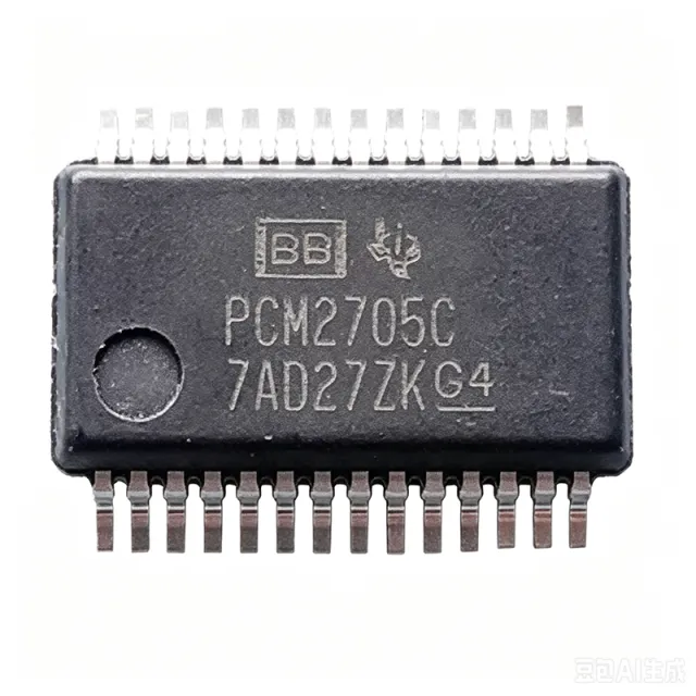
PCM2705C - 98dB SNR Stereo USB DAC with S/PDIF | Texas Instruments
The Texas Instruments PCM2705C is a single-chip stereo audio digital-to-analog converter (DAC) with an integrated USB 2.0 full-speed protocol controller and S/PDIF output. It delivers 98dB SNR and supports both bus-powered and self-powered operation with software control. The device is fully compliant with USB 2.0 specifications and USB Audio Class, requiring no dedicated device driver. It comes in a 28-pin SSOP package, making it ideal for compact audio applications. A USB audio DAC is a digital-to-analog converter that receives digital audio data from a USB host and converts it to analog audio signals. It integrates the USB interface, protocol controller, and DAC core into a single chip, simplifying system design. The PCM2705C sits in the hierarchy of audio converters, specifically as a USB audio interface IC, which is a subset of audio data converters within the broader category of mixed-signal ICs. Key features include a 98dB SNR stereo DAC, S/PDIF output, and support for both bus-powered and self-powered modes. The device also features partially programmable USB descriptors, allowing customization of vendor ID and product ID via an external SPI host. The integrated USB transceiver eliminates the need for external PHY, reducing BOM cost and board space. Technically, the PCM2705C uses adaptive isochronous transfer for audio data, ensuring synchronized playback. The S/PDIF output supports digital audio transmission to external decoders or amplifiers. The device operates from a 3.3V supply and includes an internal PLL for clock generation, minimizing external components. The SSOP-28 package provides a compact footprint suitable for portable and space-constrained designs. Typical applications include USB sound cards, docking stations, gaming headsets, and portable audio interfaces. The device's plug-and-play capability makes it ideal for consumer audio products where driver installation is undesirable. Its low power consumption and small size also suit battery-powered devices. When designing with the PCM2705C, ensure proper decoupling of the 3.3V supply and careful layout of the USB differential pair to maintain signal integrity. The SPI interface for descriptor programming should be configured during initial setup, and the PSEL and HOST pins must be set correctly for the desired operating mode.

PEF20525FV1.3 - Serial Comm Controller SEROCCO-H | Infineon
The Infineon PEF20525FV1.3 is a SEROCCO-H Serial Optimized Communications Controller IC, designed for high-performance telecommunications applications. It features two independent serial channels and provides advanced PPP/HDLC protocol handling, packaged in a 100-pin TQFP (PG-TQFP-100-3) surface-mount form factor for embedded telecom systems. A Telecom IC (also called a network controller or serial communications controller) is a specialized integrated circuit that offloads data link layer protocol processing from a host CPU. It sits between the physical layer transceiver and the host processor, implementing framing, CRC, and channel management for synchronous serial links. In the system hierarchy, it belongs to the interface IC / network controller & processor category of integrated circuits, enabling deterministic serial data flow in equipment such as ISDN terminal adapters, xDSL modems, and T/E-carrier interface cards. Key features of the PEF20525FV1.3 include two independent serial channels with full-duplex operation, integrated PPP/HDLC framing support, hardware-assisted bit processing for low host CPU overhead, and flexible clocking for T-carrier and E-carrier telecom standards. The device also offers DMA-friendly host interface options and comprehensive interrupt/status reporting, allowing tight integration with embedded host processors. The SEROCCO-H architecture combines dedicated hardware engines for HDLC/PPP framing, CRC generation and checking, and serial channel arbitration. This offloads heavy protocol processing from the host CPU, allowing the host to focus on higher-layer networking tasks. The dual-channel design enables simultaneous handling of two independent serial links, which is valuable for routers, gateways, and multi-port communication equipment. Typical applications include ISDN terminal adapters, xDSL modems, T1/E1 interface cards, frame relay equipment, and embedded telecom modules for factory or industrial networking. The wide protocol support and dual-channel capability make it suitable for any application requiring deterministic serial data link processing. When designing with the PEF20525FV1.3, ensure proper decoupling near the supply pins and follow Infineon's reference layout for the PG-TQFP-100-3 package. The host interface should be configured according to the chosen bus width and endianness to minimize glue complexity. Designers should also verify the latest firmware/driver support matrix from Infineon for their specific host processor family. This page synthesizes distributor pricing, drop-in alternatives, and practical design notes not found in the manufacturer datasheet alone.
PEF2256HV2.2 - Quad E1/T1/J1 Framer & LIU | Infineon | MQFP-80
The Infineon PEF2256HV2.2 (FALC56) is a quad E1/T1/J1 framer and line interface component (LIU) for long- and short-haul telecom applications, housed in an 80-pin P-MQFP-80-1 (Metric QFP) package. It integrates four independent framers and LIU channels on a single die, supporting both North American T1/J1 (1.544 Mbps) and European E1 (2.048 Mbps) PCM hierarchies as well as the H.100/H.110 and H-MVIP digital system highway buses for world-market telecommunication systems. A Line Interface Unit (LIU) is the analog front-end of a TDM telecom system that interfaces between the physical twisted-pair line and the digital PCM backplane. The PEF2256 quad-LIU topology places four such analog interfaces on one chip, allowing one device to terminate an entire T1/E1 quad trunk - reducing board area, BOM count, and power per channel compared with four discrete LIUs. The device belongs to the FALC56 family of framers and line interface components, itself part of the broader framer/line-interface-unit category within telecom interface ICs. Key features include programmable pulse shaping for short-haul and long-haul operation, integrated receive equalization, on-chip jitter attenuator, HDLC controllers per channel, and a flexible parallel micro-controller interface. The device handles both unipolar and bipolar line signalling and provides diagnostic loopback modes (local, remote, payload) per channel. Built-in BERT (Bit Error Rate Test) pattern generation and checking aid field deployment and production test. Typical applications include ISDN PRI (Primary Rate Interface) cards, channel banks, digital cross-connect systems, PBX trunk interfaces, cellular base station backhaul, and multi-port T1/E1/J1 line cards. With four channels per chip, designers can build a 4-port line card with one LIU, simplifying PCB layout and reducing overall system cost. When designing with the PEF2256HV2.2, ensure the analog line-side circuits (transformer, protection, termination) are placed close to the LIU pins to minimize crosstalk between the four on-chip channels. The internal jitter attenuator simplifies clock-recovery design and is configurable per channel via the microcontroller interface. This page synthesizes distributor pricing, drop-in alternatives and practical design notes that complement the manufacturer datasheet. Prices are listed as of 2026-10-09 from authorized distributors.

PEF24628EV1.2-G - Quad-Channel EFM SHDSL SoC | Infineon
The Infineon PEF24628EV1.2-G is a quad-channel EFM (Ethernet First Mile) Symmetrical High-bit-rate Digital Subscriber Line (SHDSL) transceiver System-on-Chip, integrating four independent SHDSL channels with on-chip HDLC controllers, serializer/deserializer (SerDes) interfaces, and an embedded management interface. The part is housed in a PG-LBGA-324-2 (324-pin low-profile BGA) package and operates from 1.5 V core and 3.3 V I/O supply rails. It supports the full SHDSL.bis (G.991.2) standard for symmetric DSL transmission over 2-wire copper pairs, enabling EFM bonding for aggregated multi-pair Ethernet services at the customer premises and central office. A System-on-Chip (SoC) in the telecom interface category is a highly integrated device that combines a CPU subsystem, multiple dedicated protocol engines, and a flexible host interface on a single silicon die. The PEF24628 belongs to the SHDSL/EFM transceiver SoC family, which sits hierarchically under: telecom interface IC -> wired broadband transceiver -> xDSL transceiver -> SHDSL front-end SoC. The device historically originated from the Lantiq product line, which Infineon acquired and now sells as part of its wireline communications portfolio. Key features include four independent SHDSL channels, support for EFM bonding (G.998.1), on-chip HDLC controllers, parallel and serial host interfaces, low-jitter PLL clock synthesis, and integrated line driver interface logic. The HDLC engine, parallel/serial host ports, and flexible interrupt structure minimize the burden on the external host CPU in a DSLAM line card or CPE modem design. The architecture is built on a mature 0.13 um CMOS process with mixed-signal analog front-end circuitry for the SHDSL line interface. The part includes dedicated per-channel DSP engines for SHDSL symbol processing, echo cancellation, and trellis coding. Internal SRAM buffers per channel help absorb latency variation on the host bus, and the SerDes block supports multi-channel aggregation to a framer/backhaul device. Typical applications include SHDSL.bis line cards in DSLAMs, multi-pair bonded EFM Ethernet modems, four-wire industrial DSL links, and legacy E1/T1 extension infrastructure over copper. The quad-channel density makes it a strong fit for small-form-factor CPE MDU/MTU aggregation where four bonded pairs are needed. Design consideration: pay close attention to the PG-LBGA-324-2 PCB land pattern, controlled-impedance differential routing for the SHDSL line pairs, and proper thermal management - the device dissipates significant power when all four channels are active. Reference Infineon design notes for the recommended magnetics, line protection, and host-IF timing budget. This page synthesizes distributor pricing, drop-in alternatives, and practical design notes not found in the manufacturer datasheet.

PEF2466HV2.2 - 4-Ch SICOFI Codec/Filter POTS | Infineon
The Infineon PEF2466HV2.2 is a four-channel Signal Processing Codec/Filter (SICOFI-4-µC) IC designed for Plain Old Telephone Service (POTS) line interfacing in central-office and carrier-class equipment. Housed in a P-MQFP-64-1 (64-pin Metric Quad Flat Pack) package, this telecom IC integrates four independent codec/filter channels with programmable gain, A-law/µ-law companding, and on-chip hybrid balance networks, making it a logical continuation of the well-established Siemens/Infineon SICOFI programmable codec-filter family. A codec/filter IC is a mixed-signal device that performs the analog-to-digital and digital-to-analog conversion plus the band-limiting transmit/receive filtering required to interface voice-band (300 Hz to 3.4 kHz) analog telephone lines to a digital PCM/TDM backplane such as an E1/T1 link. Within the system hierarchy, it sits between the line-side SLIC (Subscriber Line Interface Circuit) and the system-side PCM highway controller, occupying the role of a per-channel voice-band data pump in the access network. Key features include four fully independent codec/filter channels with 16-bit linear or 8-bit A-law/µ-law companded PCM coding, programmable transmit and receive gain/attenuation in 0.1 dB steps, on-chip hybrid-balance and anti-alias filters, and a serial µC or SPI control interface. The device targets 3.3 V/5 V digital supplies and a +/-5 V analog supply, supporting extended industrial temperature grades typical for outdoor or remote-cabinet telecom deployments. Architecturally, the PEF2466HV2.2 uses a sigma-delta conversion front-end per channel with dedicated switched-capacitor filters, providing flat group delay across the voice band and very low total harmonic distortion. The integrated µC interface allows per-channel gain calibration and channel-by-channel A-law/µ-law selection, eliminating external DSP overhead for companding and gain control. Typical applications include 4-channel POTS line cards in central-office switches, integrated access devices (IADs), digital loop carrier (DLC) systems, VoIP media gateways with FXS ports, and PBX line interface modules where four voice channels must be terminated in a single low-footprint device. When designing with the PEF2466HV2.2, careful attention must be paid to analog/digital ground partitioning, the PCM clock and frame-sync timing relationship, and the decoupling of the +/-5 V analog rails. The part is now in long-term supply under the Infineon (formerly Lantiq) telecom portfolio, and procurement should be planned against documented last-time-buy milestones where applicable. This page synthesizes distributor pricing, family-mate and same-package alternatives, and practical interface-design notes that complement the manufacturer datasheet with sourcing and migration context.