CI de memoria
Subcategorías
Productos (875)

K9F4G08U0B-PCB0 - 4Gbit NAND Flash, 3.3V TSOP-48 | Samsung
The Samsung K9F4G08U0B-PCB0 is a 4 Gbit (512 M x 8 bit) NAND-type flash memory IC organized as (512M + 16M) x 8 bit memory cell array with a (2K + 64) x 8 bit data register, housed in a 48-pin TSOP1 (12 mm x 20 mm) lead-free plastic thin small-outline package. It operates on a 2.7 V to 3.6 V single supply (VCC) and supports the standard x8 NAND interface with an 8-bit multiplexed I/O bus. The device is part of the K9F4G08U0B family of asynchronous, page-mode SLC NAND flash ICs intended for high-density non-volatile storage in embedded systems. A NAND flash memory is a non-volatile storage technology that retains data when power is removed and uses a NAND-connected cell array to deliver high density at low cost per bit. NAND devices expose a serial command/address/data protocol and erase in blocks, making them well suited to bulk data storage (firmware, media, logs) rather than byte-level random access. The K9F4G08U0B-PCB0 sits in the hierarchy as SLC NAND -> parallel NAND -> flash memory -> non-volatile memory -> semiconductor memory. Compared with NOR flash, NAND offers higher density and lower cost per bit at the expense of slower random read and more complex software (FTL / wear-leveling). Key features of the K9F4G08U0B-PCB0 include a 2 Kbyte (+64 byte spare) page size for read/program, automatic program and erase with on-chip page buffer, a 128 Kbyte (+4 Kbyte spare) block architecture, and standard TSOP-48 mechanical compatibility with previous-generation K9F2G08 / K9K8G08 devices. The package suffix -PCB0 indicates the 3.3 V commercial-grade lead-free TSOP1 (48-TSOP1-1220F), as opposed to the -PIB0 industrial-temperature variant or the -I / -SI 52-ball ULGA / VFBGA variants. The IC is command-set compatible with the ONFI 1.0 / legacy Samsung NAND interface family. Architecturally, the device uses a NAND string of 32 cells per bitline with page-mode read, and includes an on-chip charge pump to generate the high voltages required for program and erase. The spare 64-byte area per page is used for ECC, bad-block marking, and wear-leveling metadata; external controllers therefore typically pair this NAND with an ECC engine capable of at least 1-bit per 512-byte sector (4-bit or stronger is recommended for reliability). Typical applications include boot and bulk storage in set-top boxes, printers, industrial gateways, networking equipment, automotive infotainment, and embedded Linux / WinCE / RTOS data-logging designs. The 512 MB (x8) density is sufficient for storing firmware images, file systems (UBIFS, JFFS2, YAFFS), and large media buffers. When using this part, designers must implement software or hardware ECC, bad-block management, and block wear-leveling above the NAND; the bare IC does not include a controller. Decoupling on VCC and VCCQ with 100 nF + 1 µF capacitors placed close to the package pins is recommended. This page synthesizes distributor pricing, drop-in TSOP-48 alternatives, and practical design notes not aggregated on a single manufacturer page, including a same-package compatibility map for the K9F4G08 / K9K8G08 / K9F2G08 families.
K9K1216U0CJIB0000 - 64M x 8 / 32M x 16 NAND Flash | Samsung
The Samsung K9K1216U0CJIB0000 is a 64M x 8 bit / 32M x 16 bit NAND Flash Memory originally produced by Samsung Semiconductor and re-marketed / distributed under the Siemens branding suffix "CJIB0000". Based on the K9K1216Q0C base die, it is a member of Samsung's second-generation NAND flash family originally introduced in the early 2000s for mass-storage applications. The part carries a TSOP-I (Type 1) package form factor typical of the K9K1216 family. A NAND flash memory is a non-volatile storage technology that retains data without power by storing charge on floating-gate MOSFET cells arranged in a NAND (Not-AND) series string topology. Within the memory hierarchy, NAND flash sits below DRAM in speed but offers far higher density at lower cost per bit, making it the dominant technology for bulk data storage in consumer and industrial electronics. The K9K1216 belongs to the wider product taxonomy: NAND flash -> non-volatile memory -> memory IC -> semiconductor. The "CJIB" suffix in this MPN typically denotes a specific temperature grade, screening option, or distributor marking rather than a fundamental die variant. Key distinguishing characteristics include the 528-byte / 16-byte spare-area page architecture standard for large-block NAND of this generation, an 8-bit or 16-bit multiplexed I/O bus, on-chip command/address/data latching, automatic program and erase algorithms executed by an internal state machine, and hardware data protection during power transitions. The part operates from a single 3.3V supply typical of the K9K1216Q0C generation and supports standard NAND command sets for read (00h/30h), program (80h/10h), and block erase (60h/D0h). Typical applications include early-generation USB flash drives, MP3 players, set-top box storage, digital camera image buffers, industrial data loggers, and embedded Linux/MCU boot-and-filesystem media. The wide 16-bit data bus option enables higher throughput where the host controller can support it, while the 8-bit mode preserves compatibility with low-pin-count microcontrollers. Designers should consult the base K9K1216Q0C datasheet for full electrical characteristics, timing diagrams, and bad-block management protocol. The "0000" suffix in the CJIB0000 marking commonly indicates a tape-and-reel packaging code. For new designs, modern JEDEC eMMC or raw NAND from current Samsung lines (K9F, K9G, K9L families) are recommended, as the K9K1216 generation is no longer in active production.
K9NUGY8R6B-BCQ0 - Samsung NAND Flash Memory | Samsung Electronics
The Samsung K9NUGY8R6B-BCQ0 is a NAND flash memory device from Samsung Electronics, part of the K9NUGY family of high-density non-volatile storage ICs used in solid-state storage, embedded systems, and consumer electronics. The device stores data in NAND flash memory cells and interfaces with a host controller through a standard asynchronous NAND interface, supporting page-based read, program, and block-erase operations under control of an external memory controller. NAND flash memory is a type of non-volatile storage technology that retains data without power. Within the memory hierarchy, it sits below DRAM in speed but offers far higher density and lower cost per bit, making it the dominant technology for SSDs, eMMC storage, USB drives, memory cards, and embedded flash. Samsung is one of the world's largest NAND flash manufacturers, and the K9 family of raw NAND devices has been an industry reference for decades. Key characteristics of this device class include high storage density per package, page-oriented program and erase operations, and a command/address/data multiplexed I/O interface. Error-correcting code (ECC) handling is performed by the host controller, as raw NAND devices do not manage ECC internally. Program and erase endurance, data retention, and block organization parameters should be confirmed from the official Samsung datasheet before design-in. Typical applications include solid-state drives, embedded storage modules, set-top boxes, digital televisions, network-attached storage, industrial data loggers, and removable media. In these systems the NAND device works alongside a flash controller that manages wear leveling, bad-block management, and ECC to deliver reliable long-term storage. Design considerations include power-supply decoupling on the VCC rail, careful PCB layout of the multiplexed address/data bus for signal integrity, and respect for tWB/tRR timing parameters during program operations. Ensure the host controller ECC strength matches the datasheet requirement for the device's NAND cell technology, as newer NAND generations require stronger correction capability. This page synthesizes cross-reference candidates, application guidance, and structured sourcing data in one place, adding value beyond the raw manufacturer datasheet listing.
K9PRGY8S7M - Samsung NAND Flash Memory IC | Samsung Electronics
The Samsung Electronics K9PRGY8S7M is a NAND flash memory integrated circuit belonging to Samsung's K9-series non-volatile memory lineup, supplied in a ball grid array (BGA) surface-mount package. Based on distributor listings (IC2IC, OMO Electronic, Alibaba), this device is cataloged as a Samsung NAND FLASH component and is actively traded on the open electronics market. NAND flash is a type of non-volatile storage technology that retains data without power. Within the memory hierarchy, NAND flash sits below DRAM in speed but offers far higher density and lower cost per bit, making it the backbone of SSDs, eMMC modules, USB drives, memory cards, and embedded storage. NAND cells are arranged in series, which reduces die area and enables the multi-gigabit capacities required by modern consumer, industrial, and automotive systems. Samsung is one of the world's leading NAND producers, with its 3D V-NAND technology stacking cells vertically to increase density further. Key characteristics of the K9-series include page-based program and block-based erase operations, asynchronous or toggled-mode interfaces, and internal ECC support on newer generations. Exact density, organization, page size, block size, and interface speed for this specific ordering code are not published in the retrieved web data and must be confirmed from the official Samsung datasheet. Typical applications for this class of device include embedded storage in set-top boxes, smart TVs, industrial controllers, networking equipment, and solid-state drive assemblies where a raw NAND device is managed by a host controller or firmware layer such as FTL (Flash Translation Layer). Design teams should confirm the exact package outline, ball map, supply voltage, and timing parameters against the Samsung datasheet before layout, since K9-series ordering codes encode density, configuration, and speed grade variations. Note that one distributor listing (OMO Electronic) attributes the MPN to BURNDY, which appears to be an indexing error given the K9 prefix and multiple corroborating NAND FLASH listings for Samsung. This page synthesizes open-market sourcing data, lifecycle status, and alternative-part guidance not consolidated on any single distributor page.

K9T1G08U0M-PIB0 - 1Gbit SLC NAND Flash, TSOP-I | Samsung
The Samsung K9T1G08U0M-PIB0 is a 1 Gbit (128M x 8) single-level cell (SLC) NAND Flash memory organized as 128 megabytes by 8 bits, supplied in a 48-pin TSOP Type I package with a 2.7V-3.6V single power supply. It belongs to Samsung's K9T family of asynchronous SLC NAND devices, offering high-density non-volatile storage with 8-bit I/O bus interface and standard NAND command set compatibility. What is SLC NAND Flash? SLC (Single-Level Cell) NAND Flash stores one bit per memory cell, providing higher endurance, faster write performance, and longer data retention than MLC or TLC counterparts. NAND Flash sits in the non-volatile memory hierarchy between NOR Flash (byte-level random access) and mass storage like eMMC/SSD controllers. It is widely used as a raw storage medium paired with an external controller for error correction (ECC), bad block management, and wear leveling. SLC variants typically deliver 100,000 P/E cycles versus 1,000-3,000 for MLC, making them preferred for industrial, automotive, and embedded systems requiring long-term reliability. Key specifications of the K9T1G08U0M-PIB0 include a 1 Gbit density, x8 organization, page size of 2 Kbytes, block size of 128 Kbytes, and an on-chip page register for read/program operations. The device features an asynchronous interface with typical read access times, hardware data protection, and supports CE#-low read operations. Operating from 2.7V to 3.6V VCC, the PIB0 suffix indicates Pb-free (lead-free) compliance, and the package designation maps to TSOP Type I (48-pin, 12 mm x 20 mm body). The K9T1G08U0M-PIB0 uses a NAND string architecture with floating-gate SLC cells, an integrated page buffer, and an internal command/address state machine. The control logic accepts standard NAND command codes (00h/30h for read, 80h/10h for program, 60h/D0h for erase). The 8-bit multiplexed I/O bus carries both address, command and data, with dedicated control signals including CE#, RE#, WE#, ALE, CLE, WP#, and R/B# (Ready/Busy). Typical applications include embedded Linux boot storage, industrial data loggers, set-top box firmware, networking equipment (routers, switches), point-of-sale terminals, and automotive infotainment. The 1 Gbit density is well suited for storing bootloaders, OS images, logs, configuration, and small media files in cost-sensitive designs that need non-volatile memory without the overhead of managed flash controllers. When designing with this device, the host controller must implement hardware or software ECC (typically 1-bit per 528 bytes for legacy NAND, or 4-bit/8-bit for higher reliability). Bad block management is mandatory - factory-marked bad blocks must be skipped during initial mapping. Adequate VCC decoupling and a stable R/B# poll sequence are critical; consult the Samsung K9T1G08U0M datasheet for command timing diagrams. This page synthesizes distributor pricing, drop-in alternatives, and practical design notes not found in the manufacturer datasheet alone.
KCP556SD8-32 - 32GB DDR5 5600 SODIMM 262-pin | Kingston
The Kingston KCP556SD8-32 is a 32 GB DDR5 SO-DIMM memory module operating at 5600 MT/s (PC5-44800), housed in a 262-pin Small Outline DIMM form factor with CL46 timing at 1.1 V. It is a single-rank-per-module configuration built from 2Rx8 DRAM devices using 16 Gbit density components, and is supplied as one 32 GB module per package. A SO-DIMM (Small Outline Dual In-line Memory Module) is a compact, JEDEC-standardized memory module form factor optimized for space-constrained systems such as laptops, mini-PCs, small-form-factor desktops, and All-In-One computers. DDR5 SDRAM represents the fifth generation of double-data-rate synchronous DRAM, delivering higher per-pin bandwidth, lower operating voltage (1.1 V vs 1.2 V for DDR4), and on-die ECC support compared with its predecessors. Within the broader memory hierarchy, SO-DIMM DDR5 modules sit between soldered LPDDR and full-size DIMM DDR5 modules, offering upgradability and standardized compatibility across consumer and commercial platforms. Key features of the KCP556SD8-32 include a 5600 MT/s transfer rate (PC5-44800), 32 GB single-module capacity, Non-ECC unbuffered signaling, CL46 CAS Latency timing, 2Rx8 rank and organization, and a 1.1 V typical operating voltage compliant with JEDEC DDR5 standards. The 262-pin edge connector follows the JEDEC SODIMM standard for DDR5 modules. The KCP556SD8-32 is validated through Kingston's system-specific compatibility program for each major laptop brand, ensuring plug-and-play operation without BIOS adjustments. Its unbuffered, Non-ECC configuration makes it appropriate for mainstream consumer and commercial notebooks rather than server or workstation platforms that require ECC or registered DIMMs. Typical applications include laptop memory upgrades, mini-PC and small-form-factor desktop upgrades, All-In-One system expansion, workstation notebooks, and content-creation portable systems that benefit from higher DDR5 bandwidth for video editing and large dataset processing. When designing or upgrading with this module, confirm the target system supports DDR5 SO-DIMM at 5600 MT/s. Systems that only support lower DDR5 speeds will clock the module down to their maximum supported rate, preserving stability but reducing peak bandwidth. Mixed-module installations are supported only if both modules share identical ranks, timings, and voltage. This page synthesizes distributor pricing, validated Kingston part specifications, and practical upgrade guidance not consolidated on the manufacturer datasheet.
KF560R32RBEK8-256 - 256GB DDR5-6000 CL32 RDIMM ECC Kit | Kingston
The Kingston FURY KF560R32RBEK8-256 is a 256 GB kit of eight 32 GB DDR5-6000 CL32 registered ECC memory modules (RDIMM) engineered for next-generation Intel and AMD workstation and high-end desktop platforms that require DDR5 Registered DIMMs. The kit operates at 6000 MT/s with a CAS latency of 32 (32-38-38 timings) at 1.35 V and supports both AMD EXPO v1.1 and Intel XMP 3.0 overclocking profiles. Each module is a 4G x 80-bit (32 GB) 1Rx4 ECC SDRAM device built on twenty 4G x 4-bit FBGA components per module, providing on-die ECC plus registered parity for data integrity. DDR5 RDIMM memory represents the server-class evolution of the DDR5 standard. An RDIMM (Registered DIMM) buffers the command/address/control signals through a register clock driver on the module itself, which allows the memory controller to drive more modules per channel at higher frequencies than unbuffered DIMMs. Combined with ECC (Error-Correcting Code), RDIMMs are preferred for workstations and entry-level servers running memory-intensive workloads such as CAD/CAE simulation, 3D rendering, scientific computing, AI inference and data analytics where silent bit-flips cannot be tolerated. The Kingston FURY Renegade Pro line extends this server-class reliability with overclocked XMP/EXPO profiles, closing the historical gap between gamer memory and workstation memory. The 6000 MT/s speed with CL32 produces a first-word latency of approximately 10.667 ns, which is competitive with top-tier desktop DDR5 kits while retaining the ECC and registered signaling demanded by professional workloads. The kit populates eight DIMM slots for maximum channel parallelism on modern 8-channel workstation boards. Typical applications include content-creation workstations (video editing, color grading, VFX rendering), engineering simulation (FEA, CFD, EDA timing closure), AI development and inference workstations, and high-end desktop platforms (HEDT) that pair multi-core CPUs with RDIMM-compatible motherboards such as AMD TRX50/WRX90 and Intel W790. It is also suitable for entry-level virtualization hosts and local training servers that need large memory capacity with ECC integrity. A practical design consideration: verify that the target motherboard supports 1.35 V DDR5-6000 operation on RDIMM slots; some platforms cap RDIMM speed at 4800 or 5600 MT/s, in which case the XMP/EXPO profile will fall back to a JEDEC-compatible lower speed. Because each module uses a register clock driver, do not mix these RDIMMs with unbuffered UDIMMs on the same channel - the electrical signaling differs and mixing is unsupported. This page consolidates Kingston verified datasheet specifications, distributor pricing as of 2026-10-11, drop-in alternative kits, and practical workstation-build guidance that is not present in the manufacturer datasheet alone.
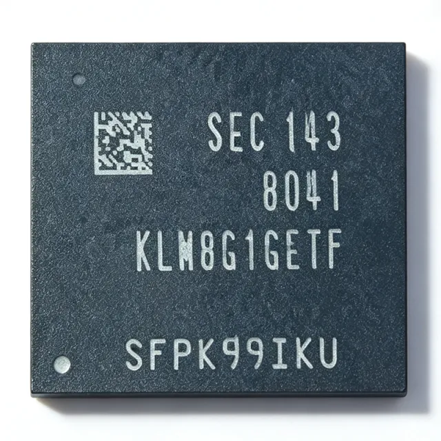
KLM8G1GETF-B041 - 8GB eMMC 5.1 Flash, 153-FBGA | Samsung
The Samsung KLM8G1GETF-B041 is an 8 GB (64 Gbit) eMMC 5.1 embedded flash storage device with MLC NAND, a 3V VDDF (NAND) supply, 1.8V/3V dual VCCQ supply, and a 153-pin FBGA package rated from -25C to +85C. An eMMC (embedded MultiMediaCard) is an embedded flash storage solution that integrates NAND flash die and a standard MMC controller in a single BGA package. It sits within the memory hierarchy as non-volatile embedded storage, managed through the JEDEC-standard MMC protocol v5.1, which presents a simple read/write register interface to the host processor instead of raw NAND management. Key features include eMMC 5.1 specification compatibility, built-in wear leveling, bad block management, ECC error correction, a hardware reset function, and secure write protection. Because the controller handles flash management internally, host software complexity is dramatically reduced compared with raw NAND. Technically, the device exposes a x1 or x4-bit or x8-bit data bus operating under MMC protocol v5.1, with VDDF at 3V for the NAND area and VCCQ at 1.8V or 3V for the interface. Samsung positions its eMMC eSTORAGE family as offering superior power efficiency and fast speed for slim mobile designs. The integrated controller performs erase management, wear leveling, and error correction transparently. Typical applications include smartphone and tablet main storage, smart home and IoT hubs, industrial HMI and data loggers, set-top boxes, and automotive infotainment head units. The 153-FBGA footprint and industry-standard interface allow drop-in swap between compliant 8GB eMMC 5.1 parts. Design consideration: verify the exact FBGA ball-map suffix, because suffix digits such as -B041 versus -B001 can encode different ball grid arrays, making physically incompatible parts that look identical on paper. This page synthesizes distributor pricing, drop-in alternative analysis, lifecycle alerts, and practical migration notes not found in the Samsung datasheet.
KM416V4104CS-L6 - 4Mx16 EDO DRAM 60ns 3.3V TSOP-50 | Samsung
The Samsung KM416V4104CS-L6 is a 4M x 16-bit CMOS Dynamic RAM with Extended Data Out (EDO) architecture, organized as 4Mx16 with 4K refresh and housed in a 50-pin TSOP Type II surface-mount package. It operates from a single 3.3V power supply and offers access times of 60ns (denoted by the '-L6' speed suffix) and 50ns (for the '-L5' speed grade variant). An EDO DRAM (Extended Data Out Dynamic Random-Access Memory) is a type of dynamic RAM that extends the period during which output data remains valid by latching the column address on the rising edge of /CAS, effectively enabling a new column access to begin before the previous data has been read. EDO sits in the memory hierarchy between Fast-Page Mode DRAM (FPM) and synchronous SDRAM, and was widely used in mid-1990s PCs, graphics cards, set-top boxes, and embedded systems before SDRAM displaced it. Key features of the KM416V4104CS-L6 include a 4M x 16 organization (64 Mbit total), 4K refresh cycles at 64ms intervals, CMOS low-power design, and TSOP-II packaging optimized for SMT assembly. The L6 grade specifies a 60ns random column access and 30ns page-mode cycle time. The device also supports CAS-before-RAS (CBR) refresh and self-refresh modes, which simplify memory controller design and reduce power consumption in standby. Typical applications for the KM416V4104CS-L6 include legacy PC main memory modules (such as the KMM366F804CS1 8Mx64 DIMM built from eight KM416V4104CS devices), set-top boxes, industrial control systems, point-of-sale terminals, embedded graphics frame buffers, and telecommunications switching equipment. The 16-bit-wide organization is well suited to bus widths common in 1990s-era microcontrollers and DSPs, including Intel i386/i486 and early PowerPC-based designs. When designing with this part, ensure proper decoupling with 0.1 uF and 0.01 uF capacitors placed near the VCC pins, maintain signal integrity on the address/control lines, and respect the 64ms refresh window. Designers should also note that KM416V4104CS-L6 is a mature, obsolete part - active designs should consider SDRAM, DDR, or modern SRAM equivalents. This page synthesizes distributor pricing, drop-in alternative cross-references, and practical design considerations not collected in a single place by the original Samsung datasheet, helping engineers source and qualify second-source options for legacy and EOL systems.
KM681000ALT-10L - 128Kx8 5V Low-Power CMOS SRAM | Samsung
The Samsung KM681000ALT-10L is a 128K x 8 bit (1 Mbit) high-speed CMOS static random-access memory (SRAM) organized as 131,072 words by 8 bits, fabricated in low-power CMOS technology and supplied in a 5V operating variant. The -10L speed suffix indicates a 100 ns address access time, suitable for cost-sensitive embedded systems where moderate access latency is acceptable. It is part of Samsung's KM681000 family of asynchronous SRAM devices designed for commercial and industrial temperature ranges. A static RAM (SRAM) is a type of volatile semiconductor memory that uses bistable latching circuitry (typically 6 transistors per cell) to store each bit, eliminating the need for periodic refresh cycles required by dynamic RAM (DRAM). SRAM occupies the role of cache, scratchpad, and buffer memory in the broader memory hierarchy: register file -> SRAM cache -> DRAM main memory -> storage. Its random-access nature and byte-level write granularity make it ideal for control logic, lookup tables, and small data buffers where speed and simplicity outweigh density-per-cost. Key features of the KM681000ALT-10L include 128K x 8 organization, 5V single-supply operation, low standby current, fully static operation requiring no clock or refresh, and TTL-compatible I/O. The device supports common asynchronous SRAM control signals (chip enable, output enable, write enable) and operates over commercial (0C to +70C) or industrial (-40C to +85C) temperature ranges depending on the device grade. The 'ALT' suffix denotes a specific package and operating-mode variant within the KM681000 family. Architecturally, the KM681000ALT-10L uses a 6T CMOS SRAM cell array, internal address decoding, and an 8-bit bidirectional data bus. The die is offered in a small-outline surface-mount package to support compact PCB layouts. The asynchronous interface simplifies integration with microcontrollers and legacy logic that do not provide dedicated SDRAM controllers. Typical applications include industrial control PLCs and HMI panels, networking equipment buffer memory, point-of-sale terminals, instrumentation data logging, automotive infotainment subsystems, and legacy embedded computing where deterministic low-latency read/write access and high endurance are required. The wide temperature tolerance and 5V supply simplify designs replacing older SRAMs in long-lifecycle products. When designing with this device, ensure the address and data lines have adequate decoupling near the device and that the chip-enable access timing (tCE) is respected in worst-case read cycles. Designers upgrading from older 5V SRAMs should confirm the pinout matches their existing footprint, as different Samsung speed grades (e.g., -8, -10, -12) share the same functional pinout but differ in access time.
KSM56R46BD8PMI - 32GB DDR5-5600 ECC RDIMM 2Rx8 CL46 | Kingston
The Kingston KSM56R46BD8PMI is a 32GB DDR5-5600 Registered ECC server memory module (RDIMM) with 2Rx8 rank organization, CL46 timing, and a 288-pin DIMM form factor operating at 1.1V. It belongs to Kingston's Server Premier product line, which provides locked BOM server memory validated on OEM platforms. A DDR5 RDIMM (Registered DIMM) is a type of server-grade synchronous DRAM module that uses an on-module register buffer between the memory controller and the DRAM chips. DDR5 (Double Data Rate 5) is the fifth generation of main-memory SDRAM, succeeding DDR4 with higher per-pin transfer rates, on-DIMM voltage regulation (PMIC), and improved channel efficiency through decision feedback equalization (DFE). Within the memory taxonomy: DDR5 SDRAM -> SDRAM -> volatile memory -> integrated circuit -> semiconductor. RDIMMs are critical for enterprise servers, workstations, and high-reliability compute platforms because the register buffer reduces electrical loading on the memory controller, enabling higher capacities and more DIMMs per channel. Key features of the KSM56R46BD8PMI include a 5600 MT/s data rate (PC5-44800), a 4G x 80-bit logical organization (32GB capacity with ECC), CL46-45-45 timings at 1.1V, on-module PMIC for voltage regulation, and a 2Rx8 dual-rank configuration. The module is based on twenty 2G x 8-bit FBGA82 components. The SPD is programmed to JEDEC standard DDR5-5600 timing, and the module uses gold contact fingers for reliable high-cycle insertion in server DIMM sockets. The KSM56R46BD8PMI uses Kingston's Server Premier validation process: each BOM revision is locked and qualified on major OEM server platforms (Dell PowerEdge, HPE ProLiant, Lenovo ThinkSystem, Supermicro). This contrasts with consumer UDIMMs which are not platform-validated. The on-DIMM PMIC handles the 1.1V regulation previously performed by the motherboard, improving power integrity under heavy load. Typical applications include enterprise server memory upgrades, workstation memory for content creation, virtualization host memory pools, in-memory database deployments, and cloud compute infrastructure. The Kingston Server Premier line is engineered specifically for system integrators and data center operators who require validated, consistent memory. When designing with KSM56R46BD8PMI, verify that the target server's memory controller and BIOS support DDR5-5600 at 2Rx8 and 32GB per-DIMM density. Mixing with 1Rx8 modules in the same channel may force downclocking. The 1.1V operating voltage is mandatory - the on-module PMIC handles regulation; do not bypass. This page synthesizes distributor pricing, drop-in alternatives, and practical design notes that go beyond the manufacturer datasheet summary. It is intended for engineers and procurement specialists specifying validated server memory for OEM deployments.

M24256-BWMN6TP - 256Kbit I2C EEPROM, 1MHz, 8-SOIC | STMicroelectronics
The STMicroelectronics M24256-BWMN6TP is a 256-Kbit (32 Kbyte) I²C-compatible serial EEPROM organized as 32 K × 8 bits, housed in an 8-pin SOIC (SO-8) package. It operates on a single supply from 2.5 V to 5.5 V, supports a 1 MHz I²C bus clock with a 450 ns access time, and includes three Chip Enable (E0, E1, E2) pins that allow up to eight devices to share the same I²C bus. An EEPROM (Electrically Erasable Programmable Read-Only Memory) is a type of non-volatile memory that retains stored data when power is removed and supports byte-level in-system writes via an electrical signal. EEPROMs sit beneath Flash in the memory hierarchy: they offer lower density but higher endurance per cell (typically 1 million write cycles for this family) and byte-level granularity, making them well suited for storing user-configurable parameters, calibration constants, device IDs, and event logs that change frequently during the lifetime of a product. The M24256-BWMN6TP integrates advanced write-protection features: a Write Protect (WP) pin that hard-locks the upper quadrant of the array, and three hardware address pins that allow bus-address configuration on the fly. The device supports both byte-write and page-write (up to 64-byte page) modes, with a built-in write-cycle completion polling mechanism that simplifies firmware. The SO-8 package is a JEDEC-standard surface-mount form factor widely accepted for industrial designs. Architecturally, the device is built on STMicroelectronics' proprietary CMOS EEPROM process, which delivers >4 million write cycles per byte and >200-year data retention. The on-chip charge pump generates the high-voltage programming pulses required to tunnel electrons through the floating gate, all managed by an internal state machine that frees the host microcontroller from page-buffer timing. Typical applications include industrial control parameter storage, consumer-set user preferences, smart-meter calibration data, automotive accessory identification, medical device log retention, and I²C port expansion on small microcontrollers that lack internal non-volatile storage. Designers choose this part when they need reliable, byte-writeable memory in a familiar 8-pin footprint. When designing with the M24256-BWMN6TP, place 0.1 µF decoupling close to VCC and respect the bus idle time (tBUF) of 0.5 µs minimum to ensure proper start-condition detection. Hardware address pins E0/E1/E2 must be tied to VCC or GND (no floating inputs allowed). This page synthesizes distributor pricing, same-family drop-in alternatives, and practical design notes for the M24256-BWMN6TP not found in the manufacturer datasheet alone.

M24C01-RMN6TP - 1Kbit I2C EEPROM, SOIC-8 | STMicroelectronics
The M24C01-RMN6TP is a 1-Kbit (128 x 8-bit) serial I2C EEPROM from STMicroelectronics, housed in an 8-pin SOIC (MN) package. It operates with a supply voltage range of 2.5V to 5.5V, supports I2C bus speeds up to 400 kHz, and features a write cycle time of 5 ms. The device is organized as 128 bytes of non-volatile memory, with a byte-write and page-write capability (up to 16 bytes per page). It includes a write protect (WC) pin for hardware data protection and a device address (E0, E1, E2) input for up to 8 devices on the same bus. An EEPROM (Electrically Erasable Programmable Read-Only Memory) is a type of non-volatile memory that can be electrically erased and reprogrammed. It is a key component in the memory hierarchy, sitting between volatile RAM and permanent storage like flash. EEPROMs are used to store small amounts of configuration data, calibration constants, and device parameters that must persist across power cycles. In the broader system, EEPROMs are part of the memory IC category, which includes ROM, RAM, and flash, and are essential for applications requiring data retention without power. Key features of the M24C01-RMN6TP include a wide operating voltage range (2.5V to 5.5V), I2C interface with clock frequencies up to 400 kHz, and a low-power design with a standby current of 1 uA (typical). The device offers a write cycle time of 5 ms, ensuring fast programming, and supports both byte and page write modes. The SOIC-8 package is industry-standard, making it easy to integrate into existing PCB designs. The device is RoHS compliant and operates over a temperature range of -40C to +85C. Technically, the M24C01 uses a floating-gate transistor architecture for non-volatile storage, with a built-in charge pump for programming. The I2C interface allows for simple two-wire communication (SCL and SDA), with the device address set via three pins (E0, E1, E2), enabling up to 8 devices on a single bus. The write protect pin (WC) provides hardware protection against accidental writes, and the device supports both sequential and random read operations. Typical applications include storing calibration data in industrial sensors, configuration parameters in consumer electronics, and system settings in automotive modules. The wide voltage range and low power consumption make it suitable for battery-powered devices, while the I2C interface simplifies integration with microcontrollers. When designing with this device, ensure proper pull-up resistors on the SCL and SDA lines (typically 4.7 kOhm) and consider the write cycle time when updating data. The WC pin should be tied to ground for normal operation or to VCC for write protection. For high-reliability applications, consider the automotive-grade variant M24C01-RMN6TP/A.
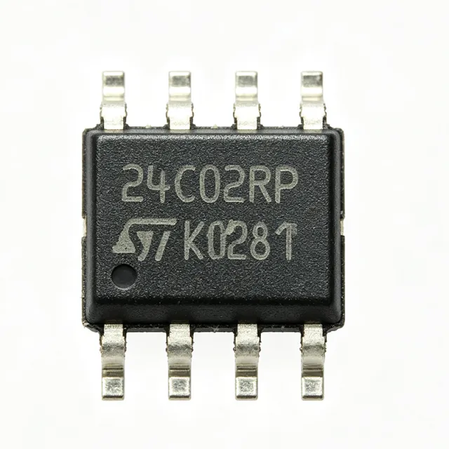
M24C02-RMN6TP - 2Kbit I2C EEPROM | STMicroelectronics
The M24C02-RMN6TP is a 2-Kbit (256 x 8-bit) serial I2C EEPROM from STMicroelectronics, housed in a compact SOIC-8 package. It operates over a supply voltage range of 1.8V to 5.5V, supports a clock frequency up to 400 kHz, and features a write cycle time of 5 ms. Data verified as of 2026-08-05. An EEPROM (Electrically Erasable Programmable Read-Only Memory) is a non-volatile memory type that retains data when power is removed, allowing byte-level erasure and reprogramming electrically. In the memory hierarchy, EEPROM sits between volatile RAM and read-only ROM, providing flexible storage for configuration parameters, calibration data, and small application logs. It is a fundamental building block in embedded systems, often interfaced via standard serial protocols like I2C or SPI. Key features include a wide operating voltage range (1.8V to 5.5V) that supports both 3.3V and 5V logic systems, a 400 kHz I2C interface for fast data transfer, and a 5 ms write cycle time for efficient programming. The device also offers a write protect pin to prevent accidental data corruption, and a page write capability of 16 bytes, enhancing programming efficiency. Its low-power consumption makes it suitable for battery-operated devices. The M24C02-RMN6TP uses a standard I2C protocol with a 7-bit device address, allowing up to eight devices on the same bus. It features a self-timed write cycle with auto-erase, simplifying the programming sequence. The device is manufactured using ST's advanced CMOS technology, ensuring high reliability and endurance of 1 million write cycles, with data retention of 40 years. Typical applications include storing calibration data in industrial sensors, configuration parameters in smart meters, and device settings in consumer electronics such as TVs and set-top boxes. Its small SOIC-8 footprint and wide voltage range make it ideal for space-constrained designs. When designing with this device, ensure proper pull-up resistors on the SDA and SCL lines (typically 4.7kΩ for 400 kHz operation) and connect the write protect pin to ground when writing is required. The device supports both byte and page write modes, with page size of 16 bytes, and acknowledges each byte during programming. This page synthesizes distributor pricing, drop-in alternatives, and practical design notes not found in the ST datasheet, providing a comprehensive resource for engineers evaluating the M24C02-RMN6TP.
M24C08-RMN6TP - 8Kbit I2C EEPROM, SOIC-8 | STMicroelectronics
The M24C08-RMN6TP is an 8-Kbit (1024 x 8) I2C-compatible serial EEPROM from STMicroelectronics, packaged in an 8-pin SOIC (N) package. It operates over a supply voltage range of 1.8V to 5.5V, making it suitable for a wide range of low-power and battery-operated applications. The device supports a clock frequency of up to 400 kHz (I2C fast mode) and features a write protect pin for hardware data protection. An EEPROM (Electrically Erasable Programmable Read-Only Memory) is a non-volatile memory that can be electrically erased and reprogrammed, retaining data without power. It is a type of memory IC that falls under the broader category of non-volatile memory, which also includes flash memory and MRAM. EEPROMs are used for storing configuration parameters, calibration data, device IDs, and small amounts of firmware that require in-system updates. The M24C08 is part of the M24Cxx family of serial EEPROMs, which are widely used in industrial, automotive, and consumer electronics. Key features of the M24C08-RMN6TP include a byte-write time of 5 ms, a write cycle endurance of 1 million write cycles, and a data retention of 40 years. The device supports both byte and page write modes (up to 16 bytes per page), and sequential read operations. It also includes a write protect (WC) pin that, when tied high, prevents write operations to the entire memory array. The device is available in a standard SOIC-8 package, which is pin-compatible with many other 8-pin EEPROMs, allowing easy drop-in replacement. The M24C08 uses a standard I2C interface with a 2-wire serial bus (SCL and SDA), and supports 7-bit device addressing with three address pins (A0, A1, A2) allowing up to eight devices on the same bus. The device is designed for low-power operation, with a standby current of 1 uA and a maximum active current of 2 mA at 400 kHz. It operates over a temperature range of -40C to +85C, making it suitable for industrial environments. Typical applications include storing calibration data in sensors, configuration settings in set-top boxes, device parameters in smart meters, and system logs in industrial controllers. The M24C08 is also used in automotive electronics for storing VIN numbers, tire pressure monitoring system (TPMS) data, and infotainment system settings. When designing with the M24C08, ensure that the SDA and SCL lines have appropriate pull-up resistors (typically 4.7 kOhm) and that the write protect pin is connected to a defined logic level. The device supports I2C fast mode (400 kHz) and is compatible with standard mode (100 kHz). For reliable operation, decouple the VCC pin with a 0.1 uF ceramic capacitor close to the device.
M24C128-RMN6TP - 128Kbit I2C EEPROM, SO-8 | STMicroelectronics
The M24C128-RMN6TP is a 128-Kbit (16K x 8) I2C-compatible EEPROM from STMicroelectronics, packaged in an 8-pin SO-8 (N) package. It operates over a supply voltage range of 1.8V to 5.5V, making it suitable for a wide variety of low-power and battery-operated applications. The device supports I2C clock frequencies up to 1 MHz (Fast-mode Plus) and features a write cycle time of 5 ms, with byte and page write modes (up to 64 bytes per page). An EEPROM (Electrically Erasable Programmable Read-Only Memory) is a non-volatile memory that retains data when power is removed, and can be electrically erased and reprogrammed. It is a type of non-volatile memory (NVM) that sits within the broader memory hierarchy, often used for storing configuration parameters, calibration data, device settings, and small amounts of firmware. EEPROMs are distinct from flash memory in that they allow byte-level erasure and programming, whereas flash typically operates on larger blocks. In a system, EEPROMs serve as a bridge between volatile RAM and permanent storage, providing a flexible and durable solution for data that must survive power cycles. Key features of the M24C128-RMN6TP include a wide operating voltage range (1.8V to 5.5V), low power consumption (standby current of 1 uA typical), and high reliability with 1 million write/erase cycles and 40-year data retention. The device also includes a write protect (WC) pin to prevent accidental writes, and supports both byte and page write operations. The I2C interface allows for easy integration with microcontrollers and other digital systems, with device addressing via three hardware pins (E0, E1, E2) to support up to 8 devices on the same bus. Technically, the M24C128-RMN6TP uses a floating-gate transistor technology for non-volatile storage, with an internal charge pump for programming. The I2C interface is compliant with the I2C bus specification, supporting standard (100 kHz), fast (400 kHz), and fast-mode plus (1 MHz) data rates. The device includes a self-timed write cycle with an internal timer, and an acknowledge polling feature to detect the completion of a write operation. The SO-8 package is a widely used surface-mount package, offering a compact footprint for space-constrained designs. Typical applications include parameter storage in industrial control systems, calibration data in medical devices, configuration settings in consumer electronics, and identification data in smart meters. The wide voltage range and low power consumption make it ideal for battery-powered IoT devices, where it can store sensor calibration and network credentials. In automotive applications, the AEC-Q100 qualified versions (M24C128-RMN6TP is not AEC-Q100 qualified, but the M24C128-RMN6TP-Q1 variant is) are used for odometer and configuration data. When designing with this device, ensure proper decoupling on the VCC pin with a 0.1 uF ceramic capacitor placed close to the device. The SDA and SCL lines should have pull-up resistors (typically 4.7 kOhm for standard mode, 2.2 kOhm for fast mode) to VCC. The write protect pin (WC) should be tied to ground for normal operation, or to VCC to protect the memory from accidental writes. For reliable operation, avoid exceeding the absolute maximum ratings, and consider the write cycle time when planning system operations.
M24C16-RMN6TP - 16Kbit I2C EEPROM, SOIC-8 | STMicroelectronics
The M24C16-RMN6TP is a 16-Kbit (2 Kbyte) serial I2C EEPROM from STMicroelectronics, organized as 2048 x 8 bits. It operates with a supply voltage range of 1.8V to 5.5V, making it suitable for a wide variety of low-power and battery-operated applications. The device is housed in an 8-pin SOIC (N) package, which is widely used in industrial and consumer electronics. An EEPROM (Electrically Erasable Programmable Read-Only Memory) is a non-volatile memory that retains data when power is removed, and can be electrically erased and reprogrammed. It is a type of non-volatile memory (NVM) that falls under the broader category of memory ICs, which also includes Flash, SRAM, and DRAM. EEPROMs are commonly used for storing configuration parameters, calibration data, device addresses, and small amounts of firmware that require in-system updates. Key features of the M24C16-RMN6TP include a 400 kHz I2C interface, a write cycle time of 5 ms, and a write protect (WC) pin for hardware data protection. It supports byte and page write modes (up to 16 bytes per page), and random and sequential read modes. The device has a typical standby current of 1 uA and an active read current of 0.5 mA, contributing to its low-power profile. It is available in a Pb-free, RoHS-compliant SOIC-8 package, with an operating temperature range of -40C to +85C. The M24C16 uses a standard I2C protocol with a 7-bit device address, where the three least significant bits (E2, E1, E0) are hardware-configurable, allowing up to eight devices on the same bus. The memory array is organized into 128 pages of 16 bytes each. The device includes a noise filter on the SCL and SDA lines to improve bus reliability in noisy environments. Typical applications include smart meters, industrial control systems, medical devices, and consumer electronics where non-volatile storage of small amounts of data is required. The wide voltage range and low power consumption make it ideal for battery-powered IoT sensors and portable devices. When designing with this device, ensure that the I2C bus pull-up resistors are properly sized for the bus capacitance and speed. The write protect pin should be tied to ground if not used, and decoupling capacitors should be placed close to the VCC pin to minimize noise.
M24C256-RMN6TP - 256Kbit I2C EEPROM, SOIC-8 | STMicroelectronics
The STMicroelectronics M24C256-RMN6TP is a 256-Kbit (32K x 8) I2C-compatible serial EEPROM with a wide operating voltage range of 1.8V to 5.5V, packaged in an 8-pin SOIC (MN) package. It features a 400 kHz clock frequency, a write cycle time of 5 ms, and a 32-byte page write capability, making it suitable for a wide range of data storage applications. An EEPROM (Electrically Erasable Programmable Read-Only Memory) is a non-volatile memory that retains data when power is removed, and can be electrically erased and reprogrammed. It is a type of non-volatile memory (NVM) that sits within the memory hierarchy between volatile RAM and permanent storage like flash. EEPROMs are used for storing configuration parameters, calibration data, device IDs, and small amounts of firmware that require in-system updates. The M24C256 is part of the M24Cxx family of I2C EEPROMs from STMicroelectronics, which are widely used in industrial, automotive, and consumer electronics. Key features include a 256-Kbit memory size, I2C interface with 400 kHz clock, 1.8V to 5.5V supply voltage, 5 ms write cycle time, 32-byte page write, and a write protect pin for hardware data protection. The device also supports sequential read and write operations, and has a 1,000,000 write/erase cycle endurance and 40-year data retention, ensuring reliable long-term data storage. The M24C256 uses a standard I2C two-wire interface (SCL and SDA) with a 7-bit device address, allowing up to 8 devices on the same bus. The device includes a write protect (WC) pin that, when tied high, prevents write operations to the entire memory array. The SOIC-8 package is industry-standard and pin-compatible with many other 256-Kbit I2C EEPROMs, enabling easy drop-in replacement in existing designs. Typical applications include storing configuration parameters in industrial sensors, calibration data in medical devices, device settings in consumer electronics, and firmware parameters in automotive ECUs. The wide voltage range and low power consumption make it suitable for battery-powered IoT devices. When designing with this device, ensure proper pull-up resistors on the SCL and SDA lines (typically 4.7kΩ for 400 kHz operation) and decouple the VCC pin with a 0.1µF ceramic capacitor. The write protect pin should be tied to ground if write protection is not needed, and the address pins (A0, A1, A2) should be tied to VCC or GND to set the device address.
M24C32-RMN6TP - 32Kbit I2C EEPROM | STMicroelectronics
The M24C32-RMN6TP is a 32-Kbit (4 Kbyte) serial EEPROM from STMicroelectronics, organized as 4096 words of 8 bits each. It operates over an I2C-compatible two-wire serial interface, supporting clock frequencies up to 400 kHz (Fast mode) and 1 MHz (Fast mode Plus) depending on the voltage range. The device is available in an 8-pin SOIC (MN) package, specifically the SO-8N (150 mil) body, and is supplied in tape and reel packaging (TP suffix). It is designed for low-power and low-voltage applications, with a wide operating voltage range of 1.8V to 5.5V, making it suitable for battery-powered and industrial systems. A serial EEPROM (Electrically Erasable Programmable Read-Only Memory) is a non-volatile memory that retains data when power is removed, and can be electrically erased and reprogrammed in-system. It is a type of EEPROM, which falls under the broader category of non-volatile memory (NVM) in the memory hierarchy. Serial EEPROMs use a serial interface (such as I2C, SPI, or Microwire) to communicate with a host controller, reducing pin count and PCB area compared to parallel EEPROMs. The M24C32 is part of the M24Cxx family of I2C EEPROMs from STMicroelectronics, which includes densities from 1 Kbit to 512 Kbit, all sharing a common command set and addressing scheme. Key features of the M24C32-RMN6TP include a write cycle time of 5 ms (typical), byte and page write modes (up to 32-byte page), and a write protect pin (WC) for hardware data protection. The device supports both sequential and random read modes, and includes an internal write protection scheme with a software write protect feature (via the WC pin). It also features a Schmitt trigger input for noise immunity and a noise filter on the SCL and SDA lines, ensuring reliable operation in electrically noisy environments. The operating temperature range is -40°C to +85°C, and the device is RoHS compliant and halogen-free. Technically, the M24C32 uses a floating-gate transistor technology for non-volatile storage, with a charge pump for programming and erasing. The I2C interface is compatible with standard, fast, and fast mode plus speeds, and the device supports 7-bit and 8-bit device addressing (with three address pins A0, A1, A2 for up to 8 devices on the same bus). The memory array is organized into 128 pages of 32 bytes each, and the device includes a self-timed write cycle with automatic erase-before-write. The write cycle time is 5 ms, and the device has an endurance of 1 million write cycles and a data retention of 40 years. Typical applications include parameter storage in industrial sensors, calibration data in medical devices, configuration storage in networking equipment, and firmware update storage in consumer electronics. The low power consumption (standby current of 1 uA) and wide voltage range make it ideal for battery-operated IoT devices and portable instruments. In an industrial sensor application, the M24C32 can store calibration coefficients and device configuration, which are read at power-up and updated periodically. When designing with this device, ensure that the I2C bus pull-up resistors are properly sized for the bus capacitance and speed. The WC pin should be tied to ground for normal write operations or to VCC for write protection. For reliable operation, decouple the VCC pin with a 0.1 uF ceramic capacitor close to the device. Also, consider the maximum write cycle time (5 ms) when planning write operations, and avoid exceeding the maximum clock frequency for the selected voltage range.
M24C512-RMN6TP - 512Kbit I2C EEPROM | STMicroelectronics
The M24C512-RMN6TP is a 512-Kbit (64K x 8) serial I2C EEPROM from STMicroelectronics, packaged in an 8-pin SOIC (SO-8) with a 200 ns write cycle time. It operates from a 1.8V to 5.5V supply voltage and supports clock frequencies up to 1 MHz, making it suitable for a wide range of data storage applications. An EEPROM (Electrically Erasable Programmable Read-Only Memory) is a non-volatile memory that retains data when power is removed, allowing for byte-level read and write operations. It is a type of non-volatile memory (NVM) within the broader memory IC category, which also includes flash memory and SRAM. EEPROMs are commonly used for storing configuration parameters, calibration data, and small amounts of firmware in embedded systems. Key features include a 512-Kbit memory size organized as 64K x 8 bits, a wide operating voltage range of 1.8V to 5.5V, and a maximum clock frequency of 1 MHz. The device supports both 100 kHz and 400 kHz I2C bus speeds, with a write cycle time of 5 ms (typical) and a write protect pin for hardware data protection. It also features a page write capability of up to 128 bytes, enhancing write efficiency. The M24C512-RMN6TP uses a standard I2C interface with a 2-wire serial bus (SCL and SDA), and includes a device address input (E0, E1, E2) allowing up to 8 devices on the same bus. The memory is organized into 512 pages of 128 bytes each, and supports sequential read and write operations. The device is manufactured using ST's advanced CMOS technology, ensuring low power consumption and high reliability. Typical applications include industrial control systems, smart meters, medical devices, and automotive electronics, where reliable non-volatile data storage is required. The wide voltage range and high clock speed make it suitable for both battery-powered and high-speed systems. When designing with this device, ensure proper decoupling capacitors on the power supply and pull-up resistors on the I2C lines. The write protect pin should be tied to ground for normal operation or to VCC to prevent accidental writes. The device is RoHS compliant and halogen-free, meeting environmental standards.

M24C64-DRMF3TG/K - 64Kbit I2C EEPROM, 1MHz, AEC-Q100 | STMicroelectronics
The STMicroelectronics M24C64-DRMF3TG/K is an automotive-grade 64-Kbit serial I2C bus EEPROM organized as 8K × 8 bits, housed in an 8-terminal MLP (2x3 mm) Wettable Flank DFN package. It operates from a 2.5V to 5.5V supply, supports a 1 MHz I2C clock with 450 ns access time, and is qualified to AEC-Q100 grade 1 for automotive applications with an operating temperature range of -40°C to +125°C. The device offers byte-level and page-level write operations, hardware write protection via the WC pin, and 4 million erase/write cycles endurance with more than 200-year data retention. An EEPROM (Electrically Erasable Programmable Read-Only Memory) is a type of non-volatile memory that retains stored data when power is removed and supports individual byte-level electrical erasure and reprogramming. In the hierarchy of non-volatile memory (EEPROM -> NVM -> memory IC -> semiconductor), I2C EEPROMs such as the M24C64 family occupy the low-density, byte-addressable niche used for configuration storage, calibration constants, and small user data sets where simplicity, low pin count, and long retention are valued over speed or density. Key features include a 1 MHz I2C / SMBus-compatible two-wire interface, a 32-byte page write buffer for fast bulk writes, hardware write-protect input, built-in ECC for single-bit error correction, and a dedicated supply monitoring block that in-progress write protection when VCC drops below threshold. The device supports both standard (100 kHz), fast (400 kHz), and fast-plus (1 MHz) I2C modes, and the selectable device address bits (A0-A2) allow up to 8 devices on a single bus. The M24C64-DRMF3TG/K uses CMOS technology with a low-power design that draws sub-microamp standby current, making it well suited for always-on subsystems in automotive ECUs, body control modules, and infotainment head units. The MLP-8 (2x3 mm) Wettable Flank package provides both small PCB footprint and automated optical inspection (AOI) capability required by automotive PCB assembly lines. Typical applications include automotive parameter storage in body and chassis modules, infotainment system configuration, smart junction box settings, battery management system (BMS) calibration data, and industrial IoT nodes requiring AEC-Q100 grade non-volatile memory. The wide 2.5V-5.5V supply range lets it interface directly with both 3.3V microcontrollers and legacy 5V systems without level translation. When designing with this device, observe the 5 ms maximum write cycle time per page and add a small polling loop in firmware to verify completion via ACK polling on the write address. The WC pin must be tied to GND for normal write operation or to VCC to permanently lock the memory array against accidental modification. Decouple VCC with a 100 nF ceramic capacitor placed within 5 mm of the supply pin.
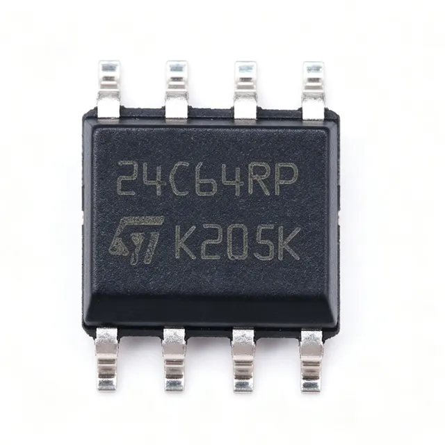
M24C64-RMN6TP - 64Kbit I2C EEPROM | STMicroelectronics
The M24C64-RMN6TP is a 64-Kbit (8K x 8) serial I2C EEPROM from STMicroelectronics, packaged in a compact SO-8 (N) package. It operates over a supply voltage range of 1.8V to 5.5V, with a maximum clock frequency of 1 MHz (for VCC >= 4.5V) and 400 kHz (for VCC >= 2.5V). The device features a byte-write time of 5 ms and a write cycle endurance of 1 million write cycles, with data retention of 40 years. Data verified as of 2026-08-05. An EEPROM (Electrically Erasable Programmable Read-Only Memory) is a non-volatile memory that can be electrically erased and reprogrammed. It is a type of memory IC that retains data when power is removed, making it essential for storing configuration parameters, calibration data, and small amounts of firmware in embedded systems. EEPROMs sit within the memory hierarchy as a non-volatile storage layer, distinct from volatile RAM and higher-capacity flash memory, and are commonly used for byte-level read/write operations in applications requiring frequent updates. Key features include a wide operating voltage range (1.8V to 5.5V), I2C interface with 7-bit device addressing, and a write protect pin for hardware data protection. The device supports sequential read and write operations, and includes a self-timed programming cycle with an internal write cycle time of 5 ms. The SO-8 package is industry-standard, enabling drop-in compatibility with many other 64-Kbit I2C EEPROMs. The M24C64-RMN6TP uses a floating-gate transistor architecture for non-volatile storage, with a charge pump for internal programming voltage generation. The I2C interface supports standard (100 kHz), fast (400 kHz), and fast-plus (1 MHz) modes, allowing flexible integration with microcontrollers. The device includes a write cycle time of 5 ms, which is typical for EEPROMs, and supports a write protect feature to prevent accidental writes. Typical applications include parameter storage in industrial sensors, calibration data in medical devices, configuration storage in networking equipment, and firmware updates in consumer electronics. The wide voltage range and low power consumption make it suitable for battery-powered IoT devices, while the high endurance (1 million cycles) supports frequent data logging. When designing with this device, ensure the I2C bus pull-up resistors are properly sized for the clock frequency and bus capacitance. The write protect pin should be tied to ground if not used, and the device address pins (A0, A1, A2) must be set to avoid conflicts with other I2C devices on the bus. This page synthesizes distributor pricing, drop-in alternatives, and practical design notes not found in the STMicroelectronics datasheet, providing a comprehensive resource for engineers selecting a 64-Kbit I2C EEPROM.

M25P16-VMF3PB - 16Mbit SPI NOR Flash 75MHz | Micron
The Micron Technology M25P16-VMF3PB is a 16 Mbit (2 Mb x 8) serial NOR Flash memory operating on an SPI-compatible bus at clock frequencies up to 75 MHz, supplied at 2.7 V to 3.6 V in a 16-pin SOP2 (16-SO) surface-mount package rated for -40 C to +125 C automotive temperature ranges. Serial NOR Flash is a non-volatile memory category that stores code and data in a NOR array architecture, allowing random access to any address through a simple serial peripheral interface (SPI). In the system memory hierarchy, it sits alongside parallel NOR and NAND Flash as a code-storage device, and is a direct descendant of the Numonyx/ST M25P family later acquired into the Micron portfolio. Compared with parallel Flash, SPI NOR reduces pin count, board area, and controller I/O requirements, which is why it dominates boot-code and firmware-storage roles in embedded designs. Key features of the M25P16-VMF3PB include its 75 MHz maximum clock frequency for fast code shadowing and XIP-style access, 2 Mb x 8 organization with 32 sectors of 64 Kbyte each (4 Kbyte subsector granularity via standard erase commands), advanced write-protection mechanisms, and deep power-down mode for minimum standby consumption. The automotive-grade suffix (PB, extended temperature) supports designs qualified to demanding environmental requirements. Architecturally, the device executes a standard SPI command set: READ and FAST_READ for data retrieval, PAGE PROGRAM for 256-byte page writes, SECTOR ERASE and BULK ERASE for content management, plus status-register and write-protect commands. The dedicated HOLD pin pauses serial communication without releasing the bus, and a hardware reset pin (S_RST on the 16-pin package) allows recovery of the serial interface. Typical applications include boot firmware storage for DSPs and microcontrollers, FPGA configuration bitstreams, parameter and calibration data storage in automotive modules, industrial drives, and set-top-box platforms. When designing with this device, verify hold times at the full 75 MHz clock and decouple VCC with 100 nF close to the supply pin; the 16-SOP2 footprint is wider than the 8-SO variant, so confirm the land pattern before second-sourcing. This page synthesizes distributor pricing, verified drop-in alternatives, and practical design notes not found in the manufacturer datasheet.
M25P16-VMF3TPB - 16Mb SPI NOR Flash 75MHz | Micron
The Micron M25P16-VMF3TPB is a 16Mb (2Mb x 8) serial NOR Flash memory with an SPI-compatible bus interface, up to 75 MHz clock support, and a 2.7V to 3.6V supply range, housed in a 16-pin SOIC wide-body (SO16W, 300 mil) package with -40C to +125C operation. Serial NOR Flash is a nonvolatile memory that stores code and data and is read over a simple four-wire SPI bus (chip select S, serial clock C, serial data input D, and serial data output Q). In the embedded-systems hierarchy it sits below parallel NOR and DRAM in bandwidth but above I2C EEPROMs in speed and density, making it the de facto standard for boot-code storage in microcontrollers, DSPs, and FPGAs. Key features of the M25P16 include 75 MHz SPI read operation, fast page programming (256-byte pages) and sector erase (64 KB sectors) with block protection, 15 ns clock-to-output access timing, and advanced write-protection mechanisms including status-register and hardware write protect. The VMF3 ordering option denotes the wide 16-pin SO package, RoHS-compliant lead-free construction, and Tape & Reel delivery, with the TP suffix indicating the shipping format. Architecturally, the device is an SLC single-level-cell NOR array organized as 2M x 8 bits, with an internal state machine that executes Read, Fast Read, Page Program, Sector Erase, Bulk Erase, and Write Status Register commands. Micron assigned this part to its Product Longevity Program, which suits multi-year industrial deployments; however, Micron has since EOL'd low-density serial NOR families, so the Renesas-published conversion guide to Adesto FUSION/Standard Flash and the cross-brand equivalents below are relevant for new sourcing. Typical applications include FPGA/DSP boot configuration (for example SHARC DSP boot loaders), BIOS/firmware storage in networking equipment, parameter and calibration data logging in industrial drives, and set-top-box or display firmware storage. Design consideration: hold the HOLD pin high and tie WRITE PROTECT appropriately; use 100 nF decoupling at VCC and respect the deep power-down entry/exit timing to minimize standby current. This page synthesizes verified distributor data, drop-in same-package alternatives, and sourcing guidance for a part affected by Micron EOL - information not consolidated in the manufacturer datasheet.