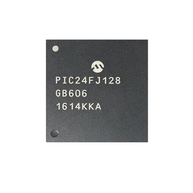
PIC24FJ128GB204-I/ML
PIC24FJ128GB204-I/ML - 16-bit XLP MCU 128KB Flash USB 44-QFN | Microchip
The Microchip Technology PIC24FJ128GB204-I/ML is a 16-bit PIC24F microcontroller with eXtreme Low Power (XLP) technology, integrating 128KB of Flash program memory, 8KB of RAM, a hardware crypto engine, and a full-speed USB 2.0 transceiver in a 44-pin QFN (8x8 mm) package. It runs up to 32 MHz, delivers 16 MIPS performance, and supports 1.8V to 3.6V operation, making it a drop-in fit for low-power secure embedded designs. According to the Microchip datasheet DS30005009C, the device is purpose-built for IoT nodes that need authenticated firmware, secure key storage, and battery-friendly standby draw. The PIC24F GB2 family is the entry point for Microchip's hardware cryptography roadmap, featuring an integrated AES engine, a true random number generator (RNG), and secure key storage.
A PIC microcontroller (MCU) is a programmable embedded processor that integrates CPU core, non-volatile Flash memory, SRAM, and peripherals (timers, ADC, communication blocks) on a single die. The PIC24F family is Microchip's 16-bit segment sitting above the 8-bit PIC16/PIC18 lines, offering higher throughput, larger address space (24-bit instruction word), and richer peripherals such as USB, crypto accelerators, and capacitive touch sensing. The eXtreme Low Power (XLP) technology adds deep-sleep modes down to nanoamp-level standby current, expanding the hierarchy: PIC24FJ -> PIC24F family -> 16-bit MCU -> microcontroller -> embedded processor -> semiconductor.
Key features of the PIC24FJ128GB204 include hardware AES-128 encryption, a true random number generator, secure key storage in OTP Flash, integrated USB 2.0 full-speed transceiver (host, device, OTG), up to 32 MHz operation (16 MIPS), 128KB Flash, 8KB SRAM, a 10-bit ADC with up to 200 ksps, multiple UART/SPI/I2C peripherals, and a real-time clock calendar (RTCC) with battery backup. The combination of crypto, USB, and XLP extends the application envelope beyond general-purpose microcontrollers into secure connected devices.
Architecturally, the PIC24FJ128GB204 uses a modified Harvard architecture with a 16-bit data path and 24-bit instruction word, plus a peripheral bus that offloads DMA transfers. The hardware crypto engine runs AES-128 in hardware without CPU intervention, accelerating secure boot and TLS handshake operations. The integrated USB PHY eliminates external transceiver components, reducing BOM cost in HID, CDC, and mass-storage designs.
Typical applications include IoT sensor nodes with secure firmware updates, USB peripherals (HID, CDC, mass storage), secure access control, smart energy metering, low-power wireless sensor hubs, medical telemetry, and consumer devices with secure boot requirements. The XLP nanoWatt technology supports multi-year battery life in sleep-dominated duty cycles.
When designing, ensure that VDD decoupling follows the 100 nF + 1 uF + 10 uF rule per Microchip's recommended layout, and route the USB DP/DM pair as a 90-ohm differential with controlled impedance. The crypto module requires secure boot firmware flow to expose its full capability.
This page consolidates distributor pricing, drop-in alternatives, and practical design notes beyond what is in the manufacturer datasheet alone.
Cotización
Contacto