SN74LVC1T45QDCKRQ1 vs SN74LVC1T45DCKR Comparación
Comparación detallada lado a lado de SN74LVC1T45QDCKRQ1 por Texas Instruments y SN74LVC1T45DCKR por Texas Instruments. Compare las especificaciones clave, los parámetros eléctricos, el encapsulado, el estado del ciclo de vida, los precios y la disponibilidad para determinar el mejor componente para los requisitos de su diseño.
Texas Instruments
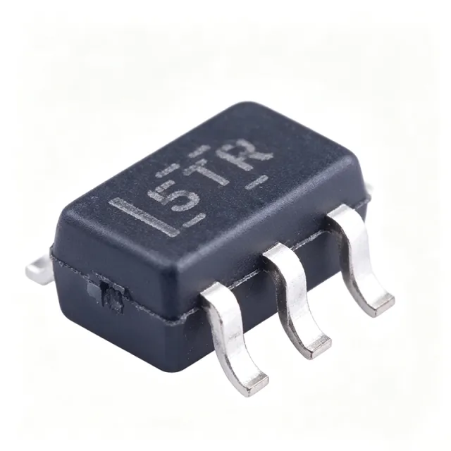
SN74LVC1T45QDCKRQ1 - Auto 1-Bit Dual-Supply Translator | TI
SN74LVC1T45QDCKRQ1 ✓ ActivoTexas Instruments

SN74LVC1T45DCKR - 420Mbps Single-Bit Dual-Supply Level Shifter | TI
SN74LVC1T45DCKR ✓ ActivoComparación de especificaciones
| Parámetro | SN74LVC1T45QDCKRQ1 | SN74LVC1T45DCKR |
|---|---|---|
| Marca | Texas Instruments | Texas Instruments |
| Categoría | Logic ICs | Logic ICs |
| Estado del ciclo de vida | Activo | Activo |
| Estado del stock | In Stock | In Stock |
| Precio unitario (USD) | $0,48 | $0,14 |
| Función | Single-bit dual-supply bus transceiver with configurable voltage translation | Single-bit dual-supply bus transceiver / voltage level translator |
| Canales | 1 channel (1-bit bidirectional) | 1 channel, bidirectional |
| Direction Control | DIR pin | DIR pin (high = A->B, low = B->A) |
| Tipo de salida | 3-State, non-inverting | — |
| VCCA Range | 1.65 V to 5.5 V | — |
| VCCB Range | 1.65 V to 5.5 V | — |
| Data Rate (max) | 420 Mbps | — |
| Propagation Delay (max) | 3.3 ns at 3.3 V | — |
| Output Drive (IOH/IOL) | +/-24 mA at 3.3 V | — |
| Quiescent Current (ICC max) | 10 uA | — |
| Input Tolerance | 5.5 V tolerant regardless of VCC | 5.5 V tolerant on both ports |
| Ioff Support | Yes (partial-power-down back-power protection) | — |
| Rango de temperatura de funcionamiento | -40 C to +125 C | — |
| AEC-Q100 Qualification | Qualified (Automotive Grade 1) | — |
| Technology | LVC CMOS | CMOS |
| Encapsulado | SC-70-6 (DCK) | SC-70-6 (DCK) |
| Tipo de montaje | Surface Mount | Surface Mount |
| Estado RoHS | Compliant | Compliant |
| Lead-Free | Yes | Yes |
| Velocidad de datos | — | 420 Mbps |
| Output Enable | — | OE pin, tri-states outputs when high |
| VCCA Supply Range | — | 1.65 V to 5.5 V |
| VCCB Supply Range | — | 1.65 V to 5.5 V |
| Logic Family | — | LVC (Low-Voltage CMOS) |
| Propagation Delay (typ @ 3.3 V) | — | 3.3 ns |
| Quiescent Current (max) | — | 10 uA |
| Output Drive (at 3.3 V) | — | ±24 mA |
| ESD Protection | — | 2000 V HBM per JESD 22 A114-A |
| VCC Isolation (Ioff) | — | Yes - both ports Hi-Z if either VCC at GND |
| Temperatura de funcionamiento | — | -40C to +85C |