SN74LVC1T45QDCKRQ1 vs SN74LVC1T45DCKR Comparison
Detailed side-by-side comparison of SN74LVC1T45QDCKRQ1 by Texas Instruments and SN74LVC1T45DCKR by Texas Instruments. Compare key specifications, electrical parameters, packaging, lifecycle status, pricing, and availability to determine the best component for your design requirements.
Texas Instruments
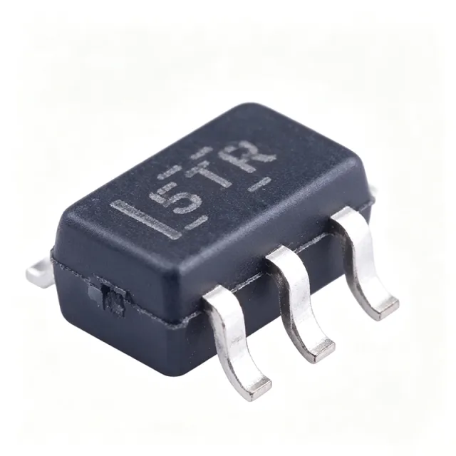
SN74LVC1T45QDCKRQ1 - Auto 1-Bit Dual-Supply Translator | TI
SN74LVC1T45QDCKRQ1 ✓ ActiveTexas Instruments

SN74LVC1T45DCKR - 420Mbps Single-Bit Dual-Supply Level Shifter | TI
SN74LVC1T45DCKR ✓ ActiveSpecification Comparison
| Parameter | SN74LVC1T45QDCKRQ1 | SN74LVC1T45DCKR |
|---|---|---|
| Brand | Texas Instruments | Texas Instruments |
| Category | Logic ICs | Logic ICs |
| Lifecycle Status | Active | Active |
| Stock Status | In Stock | In Stock |
| Unit Price (USD) | $0.48 | $0.14 |
| Function | Single-bit dual-supply bus transceiver with configurable voltage translation | Single-bit dual-supply bus transceiver / voltage level translator |
| Channels | 1 channel (1-bit bidirectional) | 1 channel, bidirectional |
| Direction Control | DIR pin | DIR pin (high = A->B, low = B->A) |
| Output Type | 3-State, non-inverting | — |
| VCCA Range | 1.65 V to 5.5 V | — |
| VCCB Range | 1.65 V to 5.5 V | — |
| Data Rate (max) | 420 Mbps | — |
| Propagation Delay (max) | 3.3 ns at 3.3 V | — |
| Output Drive (IOH/IOL) | +/-24 mA at 3.3 V | — |
| Quiescent Current (ICC max) | 10 uA | — |
| Input Tolerance | 5.5 V tolerant regardless of VCC | 5.5 V tolerant on both ports |
| Ioff Support | Yes (partial-power-down back-power protection) | — |
| Operating Temperature Range | -40 C to +125 C | — |
| AEC-Q100 Qualification | Qualified (Automotive Grade 1) | — |
| Technology | LVC CMOS | CMOS |
| Package | SC-70-6 (DCK) | SC-70-6 (DCK) |
| Mounting Type | Surface Mount | Surface Mount |
| RoHS Status | Compliant | Compliant |
| Lead-Free | Yes | Yes |
| Data Rate | — | 420 Mbps |
| Output Enable | — | OE pin, tri-states outputs when high |
| VCCA Supply Range | — | 1.65 V to 5.5 V |
| VCCB Supply Range | — | 1.65 V to 5.5 V |
| Logic Family | — | LVC (Low-Voltage CMOS) |
| Propagation Delay (typ @ 3.3 V) | — | 3.3 ns |
| Quiescent Current (max) | — | 10 uA |
| Output Drive (at 3.3 V) | — | ±24 mA |
| ESD Protection | — | 2000 V HBM per JESD 22 A114-A |
| VCC Isolation (Ioff) | — | Yes - both ports Hi-Z if either VCC at GND |
| Operating Temperature | — | -40C to +85C |