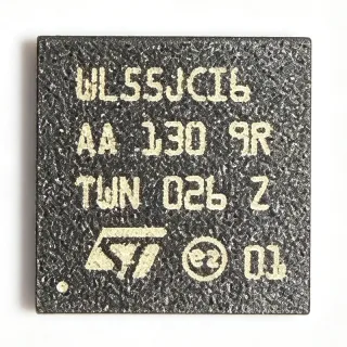
AD9371BBCZ - Dual RF Transceiver 300MHz-6GHz | Analog Devices
N.º de pieza: AD9371BBCZ ✓ Activo| Cant. | Precio unitario | Total |
|---|---|---|
| 1 | $245 | $245,00 |
| 10 | $220.5 | $2.205,00 |
| 100 | $196 | $19.600,00 |
| 500 | $171.5 | $85.750,00 |
| 1.000 | $147 | $147.000,00 |
AD9371BBCZ Descripción general
An RF transceiver is a device that combines both a transmitter and a receiver in a single package, enabling bidirectional communication over radio frequencies. The AD9371 is a system-on-chip (SoC) that integrates the RF front-end, analog-to-digital converters (ADCs), digital-to-analog converters (DACs), and digital signal processing (DSP) blocks, reducing the need for external components and simplifying system design. It sits within the hierarchy of RF transceivers -> wideband transceivers -> software-defined radio (SDR) components.
Key features include dual transmitters and receivers, support for TDD and FDD modes, and a digital interface that supports JESD204B serial data. The device offers high dynamic range and low power consumption, making it ideal for battery-powered and portable applications. It also includes an observation path for transmitter monitoring and calibration, enhancing system performance.
Technically, the AD9371 integrates fractional-N synthesizers for local oscillator (LO) generation, reducing external LO circuitry. The device supports a maximum receiver bandwidth of 100 MHz and transmitter bandwidth of 250 MHz, enabling wideband operation. It operates from a 3.3V supply and includes power management features to optimize efficiency.
Typical applications include software-defined radios, cellular base stations (3G/4G/5G), point-to-point microwave links, and military communications. Its wide frequency range and high integration make it a versatile choice for both commercial and defense systems.
When designing with the AD9371, careful attention must be paid to power supply decoupling and thermal management, as the device dissipates significant power. The JESD204B interface requires proper clocking and synchronization to ensure data integrity.
Alternativas directas para AD9371BBCZ — mismo encapsulado, compatible pin a pin. Se excluyen las piezas de otro encapsulado que requieren retrabajo de la PCB.
Variantes de esta serie
Modelos de la misma serie compatibles directamente con AD9371BBCZ (mismo factor de forma y huella) — difiere en Package, Frequency Range, Supply Voltage, Integrated Synthesizers, Type.
Herramienta de comparación rápida — seleccione piezas alternativas para compararlas lado a lado:
AD9375BBCZ
✅ Sustitución directa✓ En stock
$295 / unidad
Ver hoja de datos →AD9371BBCZ-REEL
✅ Sustitución directa✓ En stock
$147 / unidad
Ver hoja de datos →ADRV9009BBCZ
✅ Sustitución directa✓ En stock
$147 / unidad
Ver hoja de datos →ADRV9002BBCZ
✅ Sustitución directa ⚠️ Especificaciones sin verificar✓ En stock
$210 / unidad
Ver hoja de datos →AD9361BBCZ
✅ Sustitución directa ⚠️ Especificaciones sin verificar✓ En stock
$62 / unidad
Ver hoja de datos →AD9371BBCZ Especificaciones
| Type | RF Transceiver |
| Frequency Range | 300 MHz to 6 GHz |
| Number of Transmitters | 2 |
| Number of Receivers | 2 |
| Maximum Receiver Bandwidth | 100 MHz |
| Maximum Transmitter Bandwidth | 250 MHz |
| Tensión de alimentación | 3.3 V |
| Digital Interface | JESD204B |
| Encapsulado | 196-LFBGA, CSPBGA (12 mm x 12 mm) |
| Tipo de montaje | Surface Mount |
| Rango de temperatura de funcionamiento | -40C to +85C |
| Integrated Synthesizers | Yes (fractional-N) |
| Observation Path | Yes |
| TDD/FDD Support | Yes |
| Estado RoHS | Compliant |
Configuración de pines de AD9371BBCZ
| Pin A1 | GND — Ground |
| Pin A2 | VDD — Power supply |
| Pin B1 | TX1_P — Transmitter 1 positive output |
| Pin B2 | TX1_N — Transmitter 1 negative output |
| Pin C1 | RX1_P — Receiver 1 positive input |
| Pin C2 | RX1_N — Receiver 1 negative input |
| Pin D1 | TX2_P — Transmitter 2 positive output |
| Pin D2 | TX2_N — Transmitter 2 negative output |
| Pin E1 | RX2_P — Receiver 2 positive input |
| Pin E2 | RX2_N — Receiver 2 negative input |
| Pin F1 | CLK_P — Clock positive input |
| Pin F2 | CLK_N — Clock negative input |
Aplicaciones típicas
AD9371BBCZ es adecuado para 6 aplicacións: Software-Defined Radio (SDR), Cellular Base Stations (3G/4G/5G), Point-to-Point Microwave Links, Military Communications, Test and Measurement Equipment, IoT and Smart Grid.
Software-Defined Radio (SDR)
The AD9371BBCZ is ideal for SDR platforms due to its wide 300 MHz to 6 GHz frequency coverage and dual-channel architecture. Its 100 MHz receiver bandwidth and 250 MHz transmitter bandwidth support wideband waveforms, while the integrated JESD204B interface simplifies digital connectivity to FPGAs. The observation path enables real-time calibration and monitoring, enhancing SDR performance. Its low power consumption and high integration reduce board space, making it suitable for portable and fixed SDR systems.
Recomendado
Cellular Base Stations (3G/4G/5G)
The AD9371BBCZ supports TDD and FDD modes, making it suitable for cellular base stations across 3G, 4G, and sub-6 GHz 5G. Its dual transmitters and receivers enable MIMO configurations, while the integrated synthesizers reduce external LO circuitry. The 100 MHz receiver bandwidth accommodates 5G NR channel bandwidths, and the observation path supports transmitter linearization. Its high dynamic range ensures reliable performance in dense urban environments. The device's power management features help optimize efficiency in base station designs.
Recomendado
Point-to-Point Microwave Links
The AD9371BBCZ's frequency range up to 6 GHz covers many microwave link bands, and its dual-channel architecture supports full-duplex operation. The integrated fractional-N synthesizers provide precise LO generation, essential for high-frequency stability. The 250 MHz transmitter bandwidth allows wide modulation schemes, increasing data throughput. The observation path enables adaptive pre-distortion, improving link reliability. Its compact 196-ball package simplifies integration into outdoor units, and the JESD204B interface reduces digital routing complexity.
Recomendado
Military Communications
The AD9371BBCZ is suitable for military communications due to its wide frequency coverage and high integration. Its dual-channel design supports secure communication links, and the observation path enables signal monitoring and calibration. The device operates over -40C to +85C, meeting military temperature requirements. Its low power consumption is critical for portable and battery-operated military equipment. The JESD204B interface ensures robust data transfer in harsh environments, and the compact package allows for dense system integration.
Recomendado
Test and Measurement Equipment
The AD9371BBCZ is used in test and measurement equipment such as spectrum analyzers and signal generators. Its wide frequency range and high bandwidth enable accurate signal analysis and generation. The dual-channel architecture supports simultaneous transmit and receive testing. The observation path allows for real-time signal monitoring, essential for calibration. The JESD204B interface provides high-speed data transfer to processing units, and the integrated synthesizers reduce external component count. Its high dynamic range ensures precise measurements.
Recomendado
IoT and Smart Grid
The AD9371BBCZ can be used in IoT gateways and smart grid communication nodes due to its wide frequency range and low power consumption. Its dual-channel design supports redundant communication paths, enhancing reliability. The integrated synthesizers simplify frequency planning, and the JESD204B interface enables efficient data transfer to baseband processors. The observation path allows for self-calibration, reducing maintenance. Its compact package is suitable for space-constrained IoT devices, and the wide temperature range ensures operation in outdoor environments.
Recomendado
Resumen de productos recomendados
Datos de referencia de ingeniería para AD9371BBCZ — comparación, orientación de diseño e información de cumplimiento.
Guía de selección
Comparación con alternativas
| Parámetro | Este producto | AD9375BBCZ | ADRV9009BBCZ | AD9361BBCZ |
|---|---|---|---|---|
| Package | 196-LFBGA, CSPBGA | 196-LFBGA, CSPBGA | 196-LFBGA, CSPBGA | 196-LFBGA, CSPBGA |
| Brand | Analog Devices | Analog Devices | Analog Devices | Analog Devices |
| Frequency Range | 300 MHz to 6 GHz | 300 MHz to 6 GHz | 75 MHz to 6 GHz | 70 MHz to 6 GHz |
| Receiver Bandwidth | 100 MHz | 100 MHz | 200 MHz | 56 MHz |
| Transmitter Bandwidth | 250 MHz | 250 MHz | 450 MHz | 56 MHz |
| Digital Pre-Distortion (DPD) | No | Yes | Yes | No |
| Number of Transmitters | 2 | 2 | 2 | 1 |
| Supply Voltage | 3.3 V | 3.3 V | 3.3 V | 1.3 V/2.5 V/3.3 V |
Diferenciadores clave
- Wide frequency range up to 6 GHz (frente a AD9361BBCZ)
- Dual transmitters and receivers (frente a AD9361BBCZ)
- Observation path for calibration (frente a AD9361BBCZ)
Notas de diseño
The AD9371BBCZ requires a clean 3.3V supply with adequate decoupling. Use multiple 100nF and 10uF capacitors close to the power pins to minimize noise. The device has multiple power domains; ensure each is properly decoupled. Refer to the AD9371 datasheet for recommended power supply sequencing and decoupling guidelines.
The AD9371BBCZ dissipates significant power, especially during transmit. Ensure adequate thermal management by using a thermal pad and providing a solid ground plane for heat spreading. The 196-ball package has an exposed pad that must be soldered to the PCB for optimal thermal performance. Consider airflow or heatsinking for high-duty-cycle operation.
The JESD204B interface requires careful PCB layout to maintain signal integrity. Use controlled impedance traces and keep the clock and data lines matched in length. Provide proper termination and avoid routing near noisy digital lines. The datasheet provides layout recommendations for the high-speed serial interface.
Información de cumplimiento
RoHS compliant per Analog Devices product page. Not AEC-Q100 qualified as it is not an automotive component.