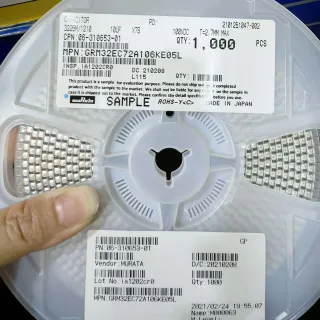
LXES03TAA1-142 - 5V Bi-Dir ESD TVS Diode, 0201 CSP | Murata
N.º de pieza: LXES03TAA1-142 ✓ Activo| Cant. | Precio unitario | Total |
|---|---|---|
| 1 | $0.42 | $0,42 |
| 10 | $0.36 | $3,60 |
| 100 | $0.28 | $28,00 |
| 500 | $0.22 | $110,00 |
| 1.000 | $0.18 | $180,00 |
| 5.000 | $0.14 | $700,00 |
LXES03TAA1-142 Descripción general
A TVS (transient voltage suppressor) diode is a solid-state semiconductor device designed to protect downstream integrated circuits from high-voltage, fast-rise-time surge events such as ESD strikes (human-body model, IEC 61000-4-2), cable-discharge events, and load-dump transients. TVS diodes occupy a position in the broader component hierarchy of protection devices (TVS diode -> ESD suppressor -> surge protector -> circuit protection -> electromechanical/component). Unlike simple Zener clamps, TVS diodes are characterized by their peak pulse current (Ipp), clamping voltage, and response time (sub-nanosecond), making them the standard defense for USB, HDMI, antenna, and sensor interfaces in modern electronics.
Key features of the LXES03TAA1-142 include its bidirectional polarity (no orientation required during PCB assembly), a typical line capacitance near 5 pF that preserves signal integrity on low-speed lines, an extremely small 0201 footprint that minimizes PCB real estate, and compliance with IEC 61000-4-2 ESD ratings. The bidirectional construction allows it to be placed across a signal line without polarity concerns, simplifying layout. The 5 pF capacitance makes it suitable for general-purpose digital lines, keypads, control buttons, and sensor I/O rather than high-speed differential pairs.
Architecturally, the LXES03TAA1-142 uses a silicon PN-junction avalanche structure optimized for low capacitance. During an ESD event, the device transitions from a high-impedance state to a low-impedance avalanche breakdown mode within sub-nanoseconds, shunting the surge current to ground and clamping the line voltage to a safe value for the protected IC. After the transient, it returns to its high-impedance state with negligible leakage. This passive, polarity-independent behavior requires no external bias or control signals.
Typical applications include automotive CAN/LIN bus protection, keyless-entry remote receivers, USB 2.0 downstream-port ESD clamps, sensor signal-line protection, and handheld/mobile device I/O protection. The AEC-Q100 qualification makes the LXES03TAA1-142 suitable for under-hood and chassis automotive modules subject to harsh EMC environments.
A critical design consideration is capacitance: at 5 pF typical the part is appropriate for sub-100 MHz signal lines but may distort signals on high-speed interfaces such as USB 3.0, HDMI, or MIPI D-PHY/CPHY. For high-speed lines, choose a sub-1 pF TVS such as the LXES15TAA1-152 family.
This page synthesizes distributor pricing, parametric alternatives, and AEC-Q100 design notes that go beyond the manufacturer datasheet to help engineers select the right Murata LXES03 ESD device for their interface.
Alternativas directas para LXES03TAA1-142 — mismo encapsulado, compatible pin a pin. Se excluyen las piezas de otro encapsulado que requieren retrabajo de la PCB.
Variantes de esta serie
Modelos de la misma serie compatibles directamente con LXES03TAA1-142 (mismo factor de forma y huella) — difiere en Breakdown Voltage (VBR min), Device Type, Number of Channels, Package, Recommended Applications.
Herramienta de comparación rápida — seleccione piezas alternativas para compararlas lado a lado:
LXES03TAA1-143
✅ Sustitución directa📋 Alternativa de referencia (no en el catálogo)
LXES03TBB1-141
✅ Sustitución directa✓ En stock
$0.0152 / unidad
Ver hoja de datos →LXES1UTAA1-157
✅ Sustitución directa✓ En stock
$0.08 / unidad
Ver hoja de datos →LXES03TAA1-142 Valores máximos y características eléctricas
| Manufacturer | Murata Manufacturing |
| Series | LXES T Series (LXES03 family) |
| Device Type | ESD Protection TVS Diode (Bidirectional) |
| Encapsulado | 2-bump CSP / DFN0603-2 (0201 / 0603 metric) |
| Package Dimensions | 1.6 mm x 0.8 mm x 0.6 mm (L x W x T, ±0.15 mm) |
| Working Voltage (Vwm) | 5 V |
| Breakdown Voltage (Vbr) | 7 V (typical) |
| Typical Capacitance | 5 pF |
| Polarity | Bidirectional |
| Tipo de montaje | Surface Mount |
| Automotive Qualification | AEC-Q100 (per Murata product spec snippet) |
| Recommended Applications | Automotive powertrain/safety equipment |
Configuración de pines de LXES03TAA1-142
| Pin 1 | Line/Bump A — Signal line or ground (bidirectional, either polarity) |
| Pin 2 | Line/Bump B — Signal line or ground (bidirectional, either polarity) |
Aplicaciones típicas
LXES03TAA1-142 es adecuado para 6 aplicacións: Automotive CAN/LIN Bus Protection, Keyless Entry / RKE Receiver Input, USB 2.0 Downstream-Port ESD Clamp, Sensor Signal-Line Protection (Analog/Digital I/O), Handheld / Mobile Device Button and Keypad ESD, Industrial Control I/O ESD Protection.
Automotive CAN/LIN Bus Protection
The LXES03TAA1-142 protects CAN and LIN automotive bus lines from ESD strikes per IEC 61000-4-2. CAN bus runs at 1 Mbit/s in high-speed mode and 125 kbit/s in fault-tolerant mode, well within the 5 pF capacitance budget of the LXES03TAA1-142. Placed between the bus line and chassis ground near the transceiver, the device clamps +/-15 kV air-discharge and +/-8 kV contact-discharge transients without distorting the bus signal. AEC-Q100 qualification makes it directly usable in under-hood ECUs and chassis modules subject to harsh automotive EMC stress. Its bidirectional operation simplifies PCB placement - either bump may sit on the line or ground side without orientation concern.
Recomendado
Keyless Entry / RKE Receiver Input
The LXES03TAA1-142 is well matched to remote keyless entry receiver antenna inputs that operate in the sub-500 MHz ISM band with low data rates (typically 1 to 20 kbps). The 5 pF typical capacitance adds negligible loading to the high-impedance antenna input while providing a robust ESD clamp against human-handle discharge events. Placed between the antenna feed and the receiver IC's RF input pin, the device returns to high-impedance state between ESD events with sub-microamp leakage. AEC-Q100 qualification supports automotive body-controller and security-module applications where the antenna pigtail may be exposed to user touch.
Recomendado
USB 2.0 Downstream-Port ESD Clamp
The LXES03TAA1-142 can clamp ESD on USB 2.0 downstream-port data lines (D+/D-) and VBUS, though with caveats. USB 2.0 high-speed runs at 480 Mbps - the 5 pF capacitance of the LXES03TAA1-142 is borderline acceptable for USB 2.0 (where the spec allows up to 10 pF of TVS loading on data pairs). Placed in parallel with each data line and biased to ground, the device clamps +/-15 kV ESD per IEC 61000-4-2. For USB 3.0 (5 Gbps) and higher, prefer a sub-0.5 pF TVS such as the LXES15TAA1-152 or TPD1E04U04 instead - the LXES03TAA1-142 is not recommended for SuperSpeed data pairs.
Recomendado
Sensor Signal-Line Protection (Analog/Digital I/O)
The LXES03TAA1-142 protects analog and digital sensor I/O pins from factory-floor and field ESD events. Sensor outputs typically run below 1 MHz and are highly sensitive to over-voltage stress, making them ideal candidates for a 5 V bidirectional TVS clamp. Placed adjacent to the sensor connector or IC pin, the LXES03TAA1-142 shunts ESD transients to ground while adding only 5 pF to the line - acceptable for 4-20 mA loop outputs, 0-10 V analog signals, and digital sensor interfaces. Its AEC-Q100 qualification extends usability to automotive sensor modules such as pressure, temperature, and position sensors.
Recomendado
Handheld / Mobile Device Button and Keypad ESD
The LXES03TAA1-142 protects push-button, keypad, and touch-input lines on handheld devices where end-user contact is expected. Buttons and keypads operate at sub-1 kHz scan rates with very high source impedance, making the 5 pF capacitance of the LXES03TAA1-142 entirely negligible. Placed adjacent to each button input pin and referenced to the device chassis ground, the LXES03TAA1-142 clamps the +/-8 kV contact-discharge and +/-15 kV air-discharge events that occur when a charged user touches a button. The 0201 CSP package fits the tightest handheld layouts.
Recomendado
Industrial Control I/O ESD Protection
The LXES03TAA1-142 protects PLC and industrial-control digital I/O channels that face cabinet-door switches, panel buttons, and field-wiring terminals. Industrial I/O typically runs at 24 V logic levels and is exposed to human-contact ESD during maintenance, but signals below 1 MHz are unaffected by the LXES03TAA1-142's 5 pF capacitance. For 24 V logic rails, pair the LXES03TAA1-142 with a higher-Vwm TVS (or confirm the 5 V rating is acceptable for the specific logic family). AEC-Q100 qualification supports industrial temperature-range operation.
Recomendado
Resumen de productos recomendados
Datos de referencia de ingeniería para LXES03TAA1-142 — comparación, orientación de diseño e información de cumplimiento.
Guía de selección
Comparación con alternativas
| Parámetro | Este producto | LXES03TAA1-143 | LXES03TBB1-141 | LXES1UTAA1-157 |
|---|---|---|---|---|
| Package | 0201 CSP (2-bump, 0.60x0.30) | 0201 CSP (2-bump, 0.60x0.30) - same | 0201 CSP (2-bump, 0.60x0.30) - same | 0201 CSP (2-bump) - same |
| Brand | Murata Manufacturing | Murata Manufacturing | Murata Manufacturing | Murata Manufacturing |
| Working Voltage (Vwm) | 5 V | 5 V | 5 V | 5 V (family datasheet) |
| Polarity | Bidirectional | Bidirectional | Bidirectional | Bidirectional |
Diferenciadores clave
- Smallest-package 5 V bidirectional TVS in Murata LXES family (frente a LXES03TBB1-141)
- AEC-Q100 qualified for automotive powertrain/safety (frente a LXES03TAA1-143)
- Bidirectional polarity for layout flexibility (frente a Unidirectional SOD-123 TVS (e.g., PESD5V0S1BA))
Notas de diseño
Place the LXES03TAA1-142 as close as possible to the connector pin or exposed signal pad to minimize the inductance path between the ESD source and the TVS clamp. Keep the trace from the protected IC pin to the TVS shorter than 3 mm where possible. Use a wide, short ground return trace directly to the chassis ground plane or the IC's GND pin - the TVS is only as effective as its ground path. Avoid routing protected traces near the board edge or near user-accessible areas where ESD is most likely to couple in.
Estimated: the 5 pF typical capacitance of the LXES03TAA1-142 may add roughly 5 percent to a 100 pF sensor load, but on a 5 pF sensor line it doubles the loading. Always simulate the RC time constant of the protected line - tau = R_source * (C_line + C_tvs) - before assuming signal integrity is preserved. Do not place the LXES03TAA1-142 on high-speed differential pairs (USB 3.0, HDMI, MIPI D-PHY) - the 5 pF capacitance will close the data eye. Choose a sub-1 pF TVS such as the LXES15TAA1-152 family for those interfaces.
The LXES03TAA1-142 0201 CSP package has a typical theta_JA in the 400-500 C/W range due to its 0.60x0.30 mm die and minimal thermal mass. During a single 8 kV contact ESD strike per IEC 61000-4-2, peak pulse currents can reach 16-30 A for sub-nanosecond durations, yielding a peak power dissipation that does NOT cause thermal runaway but does stress the solder joints. Do not run the device continuously in avalanche mode - it is designed for transient events. If the application may see sustained over-voltage, add a fuse or PTC in series.
Información de cumplimiento
AEC-Q100 qualified per Murata product specification snippet ('Automotive powertrain/safety equipment' recommended applications). RoHS and REACH compliance assumed standard for Murata LXES family - explicit certificates [DATA_NEEDED]. Halogen-free status [DATA_NEEDED].