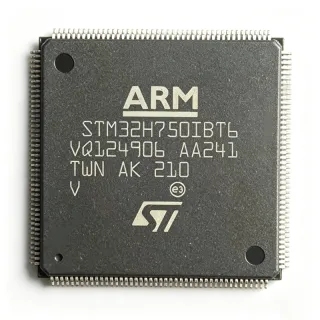
STM32F407IGT6 - 168MHz Cortex-M4 MCU 1MB Flash | STMicroelectronics
N.º de pieza: STM32F407IGT6 ✓ Activo| Cant. | Precio unitario | Total |
|---|---|---|
| 1 | $12.45 | $12,45 |
| 10 | $11.2 | $112,00 |
| 100 | $9.95 | $995,00 |
| 500 | $9.1 | $4.550,00 |
| 1.000 | $8.4 | $8.400,00 |
STM32F407IGT6 Descripción general
An LQFP, or Low-Profile Quad Flat Pack, is a surface-mount IC package with gull-wing leads on all four sides, optimized for high pin density. Microcontrollers (MCUs) like the STM32F407IGT6 belong to the embedded controller family within the broader semiconductor taxonomy: MCU -> microcontroller -> embedded processor -> integrated circuit. These devices combine a CPU core, memory, and peripherals on a single die, enabling standalone embedded systems in industrial, consumer, and automotive products.
Key features of the STM32F407IGT6 include three 12-bit ADCs (2.4 MSPS), two 12-bit DACs, 17 timers, USB OTG HS and FS, an Ethernet MAC with IEEE 1588 support, a CAN 2.0B controller, an SDMMC interface for SD cards, FSMC for external memory, a hardware crypto/hash block, and a camera interface. Up to 140 GPIO pins are exposed across the LQFP-176 footprint. Operating voltage range is 1.8V-3.6V with -40C to +85C industrial temperature range.
The Cortex-M4 core with FPU accelerates single-precision math, while the ART Accelerator eliminates Flash wait-states so CPU-bound code runs at full speed. The integrated crypto/hash accelerators (AES, Triple DES, SHA, HMAC) and true random-number generator (TRNG) support secure connectivity without external ICs. The Ethernet MAC with IEEE 1588 hardware timestamping enables industrial-grade real-time networking.
Typical applications include industrial motor control, PLCs and industrial gateways, building automation, medical instrumentation, point-of-sale terminals, multi-axis CNC, UAV flight controllers, and graphics-rich HMIs. The combination of high performance, large memory, and rich peripherals makes the STM32F407IGT6 a frequent choice for designs that outgrow Cortex-M3 resources.
When designing with this MCU, plan the clock tree carefully because the 168MHz SYSCLK requires careful PLL configuration, and ensure your debugger supports the SWD/JTAG interface. Use the STM32CubeMX tool and the HAL/LL libraries to accelerate firmware bring-up. The 176-pin LQFP is large; routing 140+ GPIOs and the Ethernet/USB differential pairs will dominate PCB area. Plan PCB layers and stackup accordingly.
This page synthesizes current distributor pricing, same-brand and cross-brand drop-in alternatives, and practical design notes not found in the manufacturer datasheet alone, helping procurement and engineering teams evaluate the STM32F407IGT6 for new designs and second-source decisions.
Alternativas directas para STM32F407IGT6 — mismo encapsulado, compatible pin a pin. Se excluyen las piezas de otro encapsulado que requieren retrabajo de la PCB.
Variantes de esta serie
Modelos de la misma serie compatibles directamente con STM32F407IGT6 (mismo factor de forma y huella) — difiere en Core Architecture, DMIPS Performance, Mounting Type, Operating Temperature Range, Package.
Herramienta de comparación rápida — seleccione piezas alternativas para compararlas lado a lado:
STM32F407IGT7
✅ Sustitución directa📋 Alternativa de referencia (no en el catálogo)
STM32F417IGT7
✅ Sustitución directa📋 Alternativa de referencia (no en el catálogo)
STM32F427IIT6
✅ Sustitución directa✓ En stock
$11.2 / unidad
Ver hoja de datos →STM32F405IGT6
✅ Sustitución directa ⚠️ Especificaciones sin verificar📋 Alternativa de referencia (no en el catálogo)
GD32F407IGT6
✅ Sustitución directa📋 Alternativa de referencia (no en el catálogo)
STM32F407IGT6 Valores máximos y características eléctricas
| Core Architecture | ARM 32-bit Cortex-M4 with FPU and DSP instructions |
| Frecuencia de reloj máxima | 168 MHz |
| DMIPS Performance | 210 DMIPS (1.25 DMIPS/MHz) |
| Program Memory (Flash) | 1 MB (1M x 8) |
| RAM Size | 192 KB |
| Encapsulado | 176-LQFP (24x24 mm) |
| Number of I/O Pins | 140 |
| Supply Voltage Range | 1.8 V to 3.6 V |
| ADC | 3 x 12-bit, 2.4 MSPS |
| DAC | 2 x 12-bit |
| Timers | 17 (general-purpose, advanced-control, basic, watchdog, SysTick) |
| Communication Interfaces | USB OTG HS/FS, Ethernet MAC (IEEE 1588), 3x SPI, 2x I2S, 3x I2C, 6x USART, 2x UART, 2x CAN 2.0B, SDMMC, FSMC, camera interface |
| Rango de temperatura de funcionamiento | -40 C to +85 C |
| Tipo de montaje | Surface Mount |
| Estado RoHS | Compliant (ROHS3) |
| Packaging (factory) | Tray |
Guía de configuración de pines de STM32F407IGT6 176-lqfp (24x24 mm)
Configuración de pines para STM32F407IGT6 (encapsulado 176-lqfp (24x24 mm)). Este CI digital incluye GPIO, interfaces de comunicación (UART, SPI, I2C) y pines de alimentación. Consulte la hoja de datos del fabricante para conocer las funciones alternativas de los pines y las opciones de configuración. Esencial para el diseño de sistemas embebidos y el diseño de PCB.

No hay datos detallados de patillaje disponibles para STM32F407IGT6.
Consulte la hoja de datos para ver la configuración completa de patillas.
Aplicaciones típicas
STM32F407IGT6 es adecuado para 6 aplicacións: Industrial Motor Control and Drives, Industrial Gateway and PLC, Medical Monitoring and Diagnostic Devices, UAV Flight Controller and Drones, Graphics HMI and TFT Displays, Audio Processing and USB Audio Interfaces.
Industrial Motor Control and Drives
The STM32F407IGT6 is a strong fit for three-phase motor control thanks to its 168 MHz Cortex-M4 with FPU that executes FOC (field-oriented control) math in hardware single-precision, plus 17 timers including advanced-control timers with complementary PWM and dead-time insertion for safe inverter drive. The three 12-bit ADCs at 2.4 MSPS sample phase currents simultaneously with the timer triggers, which is essential for sensorless and sensored FOC. The 1 MB Flash holds motor-control libraries plus a web dashboard; 192 KB SRAM accommodates trajectory buffers and the Ethernet MAC with IEEE 1588 hardware timestamping synchronizes multi-axis drives over EtherCAT-style networks.
Recomendado
Industrial Gateway and PLC
For industrial Ethernet gateways the STM32F407IGT6 brings a hardware IEEE 1588 MAC and dual CAN 2.0B controllers that bridge fieldbus devices to TCP/IP networks at line rate without external protocol ICs. The Cortex-M4 with FPU executes protocol stacks such as Modbus, PROFINet, and EtherNet/IP at 168 MHz with cycle headroom for application logic. The 1 MB Flash stores full TCP/IP stacks (lwIP) plus TLS libraries, and the 192 KB SRAM comfortably buffers packet buffers. The 176-pin LQFP exposes enough GPIOs for parallel buses, status LEDs, and isolated digital inputs typical of PLC backplanes.
Recomendado
Medical Monitoring and Diagnostic Devices
The STM32F407IGT6 is well suited to mid-tier medical devices such as multipara patient monitors, infusion pumps, and portable spirometers because the Cortex-M4 FPU executes DSP filter routines (FIR, IIR, FFT) for ECG and pulse-oximetry signal conditioning at 168 MHz without offloading to a DSP. The three 12-bit ADCs at 2.4 MSPS digitize multi-lead biopotential channels simultaneously. The hardware crypto accelerators and FSMC bus enable secure data logging to external SRAM or SD cards via SDMMC. Operating temperature -40C to +85C and the mature ST toolchain accelerate IEC 62304-compliant firmware development for medical software classes.
Recomendado
UAV Flight Controller and Drones
For UAV flight controllers the STM32F407IGT6's 168 MHz Cortex-M4 with FPU and DSP instructions runs full PID plus quaternion-based attitude control loops at 1 kHz to 8 kHz update rates with deterministic latency from the ART Accelerator (0-wait-state Flash). The 17 timers include general-purpose timers usable for input capture from RC receivers and PWM output to ESCs. The three 12-bit ADCs simultaneously sample IMU gyroscope/accelerometer/magnetometer channels. The 1 MB Flash hosts the PX4 or ArduPilot firmware plus a bootloader, while 192 KB SRAM holds state estimators and the USB OTG HS connects to a host ground-station or companion computer for HD video.
Recomendado
Graphics HMI and TFT Displays
For graphics HMIs the STM32F407IGT6's 168 MHz core with FPU accelerates JPEG decoding and LTDC (LCD-TFT controller) framebuffer compositing without an external GPU, while the FSMC bus connects 16-bit parallel TFT displays directly. The 1 MB Flash stores multilingual UI strings and bitmap assets; the 192 KB SRAM can hold an 800x480 1bpp monochrome framebuffer or partial RGB565 buffers. The SDMMC interface boots splash screens and asset packs from microSD cards. The Chrom-ART (DMA2D) hardware block offloads rectangle-copy and pixel-format conversion, freeing the CPU for application logic and touch input handling.
Recomendado
Audio Processing and USB Audio Interfaces
For USB audio interfaces and DSP effects units the STM32F407IGT6's USB OTG HS supports 480 Mbps USB 2.0 high-speed audio class 2.0 streaming at low latency. The Cortex-M4 DSP instructions and FPU run biquad filters, compressors, and reverb algorithms in real time at 168 MHz. The I2S interfaces connect to S/PDIF transceivers and audio DACs, while the SDMMC interface stores presets and IR samples. The 1 MB Flash accommodates factory presets and bootloader code; the 192 KB SRAM buffers audio frames. The hardware crypto block (when using STM32F417IGT7) protects license/authentication for commercial audio plugins.
Recomendado
Resumen de productos recomendados
Datos de referencia de ingeniería para STM32F407IGT6 — comparación, orientación de diseño e información de cumplimiento.
Guía de selección
Comparación con alternativas
| Parámetro | Este producto | STM32F407IGT7 | STM32F417IGT7 | STM32F427IIT6 | STM32F405IGT6 | GD32F407IGT6 |
|---|---|---|---|---|---|---|
| Brand | STMicroelectronics | STMicroelectronics | STMicroelectronics | STMicroelectronics | STMicroelectronics | GigaDevice |
| Package | 176-LQFP (24x24 mm) | 176-LQFP (24x24 mm) - same | 176-LQFP (24x24 mm) - same | 176-LQFP (24x24 mm) - same | 176-LQFP (24x24 mm) - same | 176-LQFP (24x24 mm) - same |
| Core | Cortex-M4F 168 MHz | Cortex-M4F 168 MHz | Cortex-M4F 168 MHz | Cortex-M4F 180 MHz | Cortex-M4F 168 MHz | Cortex-M4F 168 MHz |
| Flash | 1 MB | 1 MB | 1 MB | 2 MB | 1 MB | 1 MB |
| SRAM | 192 KB | 192 KB | 192 KB | 256 KB | 192 KB | 192 KB |
| Operating Temperature | -40C to +85C | -40C to +105C | -40C to +105C | -40C to +85C | -40C to +85C | -40C to +85C |
| Ethernet MAC | Yes (IEEE 1588) | Yes (IEEE 1588) | Yes (IEEE 1588) | Yes (IEEE 1588) | No | Yes |
| Crypto / Hash Accelerator | No (F407 has no crypto block) | No | Yes (AES, SHA, HMAC, TRNG) | Yes (AES, SHA, HMAC, TRNG) | No | No (software only) |
| DMIPS | 210 DMIPS | 210 DMIPS | 210 DMIPS | 225 DMIPS | 210 DMIPS | ~210 DMIPS |
Diferenciadores clave
- Adds hardware crypto/hash (AES/SHA/HMAC) and TRNG versus STM32F407 (frente a STM32F417IGT7)
- Higher 180 MHz clock and 2 MB Flash for headroom (frente a STM32F427IIT6)
- Lower-cost register-level clone for cost-sensitive second-source (frente a GD32F407IGT6 (GigaDevice))
Notas de diseño
Power the STM32F407IGT6 from a 3.3V LDO capable of at least 250 mA (peak current during Flash programming and Ethernet activity can spike higher than the datasheet typical). Add bulk 4.7uF and 100nF decoupling on each VDD pin pair. Place the 100nF caps within 2 mm of each VDD pin to suppress the 168 MHz core switching transients. The VBAT pin can be tied to a coin-cell or supercap for RTC and backup-register retention across power cycles; isolate it from VDD with a Schottky diode.
Route the HSE 8 MHz crystal traces within 5 mm of the OSC_IN/OSC_OUT pins, guard them with a ground ring, and keep them away from switching power and high-current traces. The USB OTG HS D+/D- differential pair must be 90 ohm impedance-controlled with length matching within 150 mil. The Ethernet MII/RMII signals to the external PHY must be length-matched within 50 mil and routed as a bus with continuous ground reference - any impedance discontinuity will cause CRC errors at 100 Mbps.
Do not assume all STM32F407 variants include the Ethernet MAC - the F405 family lacks the MAC and camera interface, while the F417/F427 families add crypto/hash blocks. Verify the silicon revision (cut A vs cut B) because some errata affect USB HS and Ethernet on early revisions. The BOOT0 pin must be pulled low for normal boot, pulled high for system-memory bootloader; add a 10 kohm pulldown plus a test-point to recover from misprogramming. The 1 MB Flash exceeds the linker-default 768 KB region; explicitly set the linker scatter file to span 0x08000000-0x080FFFFF.
Información de cumplimiento
ROHS3 compliant per distributor product page and PartGenie datasheet. Industrial temperature grade (-40C to +85C); for AEC-Q100 automotive designs consider STM32F407IGT7 or a dedicated automotive-grade variant. Halogen-free status not explicitly stated in the verified web data and is set to 'unknown' to avoid fabrication.