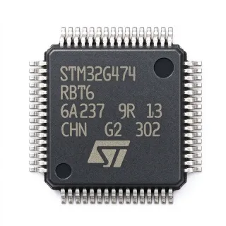
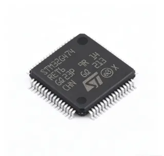
STM32L496RGT3 - Ultra-Low-Power ARM Cortex-M4 MCU 80MHz 1MB Flash | STMicroelectronics
N.º de pieza: STM32L496RGT3 ✓ Activo| Cant. | Precio unitario | Total |
|---|---|---|
| 1 | $12.8 | $12,80 |
| 10 | $11.95 | $119,50 |
| 100 | $10.85 | $1.085,00 |
| 500 | $9.65 | $4.825,00 |
| 1.000 | $8.95 | $8.950,00 |
STM32L496RGT3 Descripción general
An ultra-low-power microcontroller (MCU) is a class of microcontrollers engineered to minimize active and standby power consumption, typically using sub-threshold transistor design, multiple low-power modes (Sleep, Stop, Standby, Shutdown), and integrated DC-DC converters. The STM32L4 family sits in the broader hierarchy of ARM Cortex-M microcontrollers (Cortex-M0/M0+/M3/M4/M7/M33) under the STMicroelectronics STM32 product line, which serves industrial, IoT, medical, and consumer embedded applications where battery life is critical.
Key features of the STM32L496RGT3 include the Cortex-M4 core with single-precision FPU and DSP instructions, 1 MB Flash and 320 KB SRAM, integrated USB OTG FS, an LCD-TFT controller (8x40 or 4x44 with step-up), AES-256 hardware encryption, a true random number generator (TRNG), DFSDM (digital filter for sigma-delta modulators), and an external SMPS support interface for direct connection to an integrated switching mode power supply.
The architecture combines an ART Accelerator (Adaptive Real-Time memory accelerator) for 0-wait-state execution from Flash, a Chrom-ART Accelerator for 2D graphics offload, and 12-bit ADC and DAC peripherals. The 80 MHz Cortex-M4 core delivers 100 DMIPS / 273 CoreMark performance while the L4 series achieves an industry-leading ULPBench score of 245, reflecting its ultra-low-power efficiency.
Typical applications include wearable health devices, smart sensors, industrial HMI panels with LCD displays, USB-powered portable instruments, secure IoT endpoints with AES-256, low-power RF transceivers, and battery-backed metering systems. The 64-pin LQFP package provides ample GPIO and is suitable for hand-solderable prototypes.
When designing with the STM32L496RGT3, select the appropriate low-power mode per the application duty cycle (Shutdown for idle months, Stop for sub-second wake, Standby for RTC-only operation), and follow ST's AN4621 reference for SMPS external inductor selection. The QFP64 footprint enables easy migration to other STM32L4-series devices in the same package.
This page synthesizes distributor pricing, drop-in alternatives, and practical design notes not found in the manufacturer datasheet. Engineers should cross-check the QFP64 pinout against the STM32L496RG reference manual (RM0354) before board bring-up.
Alternativas directas para STM32L496RGT3 — mismo encapsulado, compatible pin a pin. Se excluyen las piezas de otro encapsulado que requieren retrabajo de la PCB.
Variantes de esta serie
Modelos de la misma serie compatibles directamente con STM32L496RGT3 (mismo factor de forma y huella) — difiere en Package, Performance, ADC, Core Architecture, LCD Controller.
Herramienta de comparación rápida — seleccione piezas alternativas para compararlas lado a lado:
STM32L496RGT6
✅ Sustitución directa✓ En stock
$6.5 / unidad
Ver hoja de datos →STM32L4A6RGT6
✅ Sustitución directa✓ En stock
$9.56 / unidad
Ver hoja de datos →STM32L476RGT6
✅ Sustitución directa✓ En stock
$3.86 / unidad
Ver hoja de datos →STM32L4R7VIT6
✅ Sustitución directa📋 Alternativa de referencia (no en el catálogo)
STM32L496RGT3 Valores máximos y características eléctricas
| Core Architecture | ARM Cortex-M4 with FPU and DSP |
| Frecuencia de reloj máxima | 80 MHz |
| Performance | 100 DMIPS / 273 CoreMark |
| Program Memory (Flash) | 1 MB (1M x 8) |
| SRAM | 320 KB |
| Supply Voltage Range | 1.71 V to 3.6 V |
| Rango de temperatura de funcionamiento | -40 C to +85/105/125 C |
| Shutdown Mode Current | 25 nA (5 wakeup pins) |
| VBAT Mode Current | 320 nA (RTC + 32x32-bit backup registers) |
| Encapsulado | 64-pin LQFP (10x10 mm) |
| Tipo de montaje | Surface Mount |
| USB | USB OTG Full-Speed |
| LCD Controller | 8x40 or 4x44 segments with step-up |
| Hardware Encryption | AES-256, TRNG |
| DFSDM | Yes (digital filter for sigma-delta modulators) |
| External SMPS Support | Yes |
| Estado RoHS | Compliant |
Configuración de pines de STM32L496RGT3
| Pin 1 | PB10 — GPIO/TIM2_CH3/I2C2_SCL/USART3_TX |
| Pin 2 | PB11 — GPIO/TIM2_CH4/I2C2_SDA/USART3_RX |
| Pin 3 | VSS — Ground |
| Pin 4 | VDD — Digital supply voltage |
| Pin 5 | PB12 — GPIO/SPI2_NSS/USART3_CK/LCD_COM0 |
| Pin 6 | PB13 — GPIO/SPI2_SCK/USART3_CTS/LCD_COM1 |
| Pin 7 | PB14 — GPIO/SPI2_MISO/TIM15_CH1/LCD_COM2 |
| Pin 8 | PB15 — GPIO/SPI2_MOSI/TIM15_CH2/LCD_COM3 |
| Pin 9 | PA8 — GPIO/TIM1_CH1/USART1_CK/RCC_MCO |
| Pin 10 | PA9 — GPIO/TIM1_CH2/USART1_TX/LCD_COM4 |
| Pin 11 | PA10 — GPIO/TIM1_CH3/USART1_RX/LCD_COM5 |
| Pin 12 | PA11 — GPIO/USART1_CTS/USB_DM/CAN1_RX |
| Pin 13 | PA12 — GPIO/USART1_RTS/USB_DP/CAN1_TX |
| Pin 14 | PA13 — GPIO/SYS_JTMS-SWDIO |
| Pin 15 | VSS — Ground |
| Pin 16 | VDD — Digital supply voltage |
| Pin 17 | PA14 — GPIO/SYS_JTCK-SWCLK |
| Pin 18 | PA15 — GPIO/SYS_JTDI/TIM2_CH1 |
| Pin 19 | PB3 — GPIO/SYS_JTDO/TIM2_CH2 |
| Pin 20 | PB4 — GPIO/SYS_JTRST/TIM3_CH1 |
| Pin 21 | PB5 — GPIO/TIM3_CH2/I2C1_SMBA |
| Pin 22 | PB6 — GPIO/USART1_TX/I2C1_SCL/TIM4_CH1 |
| Pin 23 | PB7 — GPIO/USART1_RX/I2C1_SDA/TIM4_CH2 |
| Pin 24 | BOOT0 — Boot mode selection |
| Pin 25 | PB8 — GPIO/TIM4_CH3/I2C1_SCL/CAN1_RX |
| Pin 26 | PB9 — GPIO/TIM4_CH4/I2C1_SDA/CAN1_TX |
| Pin 27 | VSS — Ground |
| Pin 28 | VDD — Digital supply voltage |
| Pin 29 | PC13 — GPIO/RTC_TAMP1/RTC_OUT |
| Pin 30 | PC14 — GPIO/RTC_OSC32_IN/OSC32_IN |
| Pin 31 | PC15 — GPIO/RTC_OSC32_OUT/OSC32_OUT |
| Pin 32 | VSS — Ground |
| Pin 33 | VDD — Digital supply voltage |
| Pin 34 | OSC_IN — External oscillator input (HSE) |
| Pin 35 | OSC_OUT — External oscillator output (HSE) |
| Pin 36 | NRST — Reset input (active low) |
| Pin 37 | VSSA — Analog ground |
| Pin 38 | VDDA — Analog supply voltage |
| Pin 39 | PA0 — GPIO/TIM2_CH1/TIM5_CH1/ADC_IN5 |
| Pin 40 | PA1 — GPIO/TIM2_CH2/TIM5_CH2/ADC_IN6 |
| Pin 41 | PA2 — GPIO/TIM2_CH3/USART2_TX/ADC_IN7 |
| Pin 42 | PA3 — GPIO/TIM2_CH4/USART2_RX/ADC_IN8 |
| Pin 43 | VSS — Ground |
| Pin 44 | VDD — Digital supply voltage |
| Pin 45 | PA4 — GPIO/SPI1_NSS/USART2_CK/ADC_IN9 |
| Pin 46 | PA5 — GPIO/SPI1_SCK/TIM2_CH1/ADC_IN10 |
| Pin 47 | PA6 — GPIO/SPI1_MISO/TIM3_CH1/ADC_IN11 |
| Pin 48 | PA7 — GPIO/SPI1_MOSI/TIM3_CH2/ADC_IN12 |
| Pin 49 | PB0 — GPIO/TIM3_CH3/ADC_IN15 |
| Pin 50 | PB1 — GPIO/TIM3_CH4/ADC_IN16 |
| Pin 51 | PB2 — GPIO/RTC_TAMP |
| Pin 52 | VSS — Ground |
| Pin 53 | VDD — Digital supply voltage |
| Pin 54 | PC0 — GPIO/ADC_IN1/LCD_SEG18 |
| Pin 55 | PC1 — GPIO/ADC_IN2/LCD_SEG19 |
| Pin 56 | PC2 — GPIO/ADC_IN3/LCD_SEG20 |
| Pin 57 | PC3 — GPIO/ADC_IN4/LCD_SEG21 |
| Pin 58 | VREF+ — ADC reference voltage |
| Pin 59 | VDDA — Analog supply voltage |
| Pin 60 | PA0_C — GPIO/ADC_IN5 (alternate) |
| Pin 61 | PA1_C — GPIO/ADC_IN6 (alternate) |
| Pin 62 | VSS — Ground |
| Pin 63 | VDD — Digital supply voltage |
| Pin 64 | VBAT — Battery backup supply for RTC |
Aplicaciones típicas
STM32L496RGT3 es adecuado para 6 aplicacións: Wearable Health & Fitness Devices, Smart Sensor IoT Endpoints, Industrial HMI Panels with Segment LCD, USB-Powered Portable Instruments, Battery-Backed Metering & Data Loggers, Secure Payment & Access Terminals.
Wearable Health & Fitness Devices
The STM32L496RGT3's 25 nA Shutdown mode and Cortex-M4 DSP make it ideal for wearable health monitors measuring heart rate, SpO2, and motion. Its DFSDM peripheral accepts direct sigma-delta modulator input from PPG/ECG analog front-ends, eliminating an external ADC and reducing BOM by ~$1. The integrated 12-bit ADC supports up to 5.33 MSps for high-fidelity biosignal sampling, while 320 KB SRAM buffers full waveform analysis before compression. Ultra-low-power Run mode at 2 MHz delivers 100 uA/MHz, enabling days of continuous monitoring on a single CR2032 cell. The same 64-LQFP package enables compact PCB designs under 25 mm x 25 mm.
Recomendado
Smart Sensor IoT Endpoints
IoT endpoints with secure cloud connectivity benefit from the STM32L496RGT3's AES-256 hardware encryption and true random number generator (TRNG), which offload TLS handshake and message authentication without CPU overhead. The 80 MHz Cortex-M4 core runs MQTT-SN or CoAP stacks comfortably while the Stop mode (with RTC retention) draws only 1.1 uA — enabling years of battery life on a 2400 mAh LiSOCl2 cell. External SMPS support reduces core current by 30% versus internal LDO regulation. USB OTG FS enables direct provisioning in the field without an external programmer.
Recomendado
Industrial HMI Panels with Segment LCD
The integrated segment-LCD controller (8x40 or 4x44 segments with built-in step-up converter) lets the STM32L496RGT3 drive a 4-digit numeric or 40-segment alpha display directly, eliminating an external LCD driver IC and saving both BOM cost and PCB area. The Chrom-ART Accelerator handles 2D graphics on TFT panels when used as the system HMI controller. Combined with 1 MB Flash for multilingual UI assets and 320 KB SRAM for touch-screen buffer management, the L496RGT3 supports rich industrial panel UIs while sipping power — Shutdown mode draws 25 nA for backup clock display when the main UI is off.
Recomendado
USB-Powered Portable Instruments
USB-powered portable test equipment leverages the STM32L496RGT3's integrated USB OTG Full-Speed peripheral for direct PC connectivity without an external PHY, plus its 80 MHz / 100 DMIPS performance for real-time DSP. The 12-bit 5.33 MSps ADC pairs with the on-chip op-amps for sensor conditioning, while the DAC channels drive stimulus signals. Operating from USB VBUS (5 V) through the internal LDO down to 3.3 V, the MCU draws 100 uA/MHz in Run mode — fine for tethered instruments but Switchable via Stop mode when running on battery. AES-256 secures measurement logs at rest.
Recomendado
Battery-Backed Metering & Data Loggers
Smart meters and remote data loggers benefit from the STM32L496RGT3's 320 nA VBAT mode that retains the RTC and 32x32-bit backup registers while the main domain is powered down. This enables the device to keep accurate time-stamping through years of storage without draining the backup cell. The 1 MB Flash stores months of measurement logs with wear-leveling FTL, while 320 KB SRAM caches active data. Anti-tamper detection via the integrated TRNG and AES-256 protects metering integrity against external manipulation, meeting IEC 62053 security guidelines for utility metering.
Recomendado
Secure Payment & Access Terminals
Payment terminals and access-control devices rely on the STM32L496RGT3's AES-256 hardware crypto accelerator, true random number generator, and secure boot via ST's SBSFU (Secure Boot and Firmware Update) library for PCI PTS compliance. The Cortex-M4 FPU accelerates RSA/ECC operations while keeping cryptographic key material in protected Flash regions. USB OTG FS supports PIN pad peripherals, while segment-LCD displays transaction amounts. Low-power Shutdown mode (25 nA) preserves battery backup during shipping/storage between deployments, ensuring devices arrive with full charge.
Recomendado
Resumen de productos recomendados
Datos de referencia de ingeniería para STM32L496RGT3 — comparación, orientación de diseño e información de cumplimiento.
Guía de selección
Comparación con alternativas
| Parámetro | Este producto | STM32L496RGT6 | STM32L4A6RGT | STM32L476RGT6 |
|---|---|---|---|---|
| Package | 64-LQFP (10x10) | 64-LQFP (10x10) - same | 64-LQFP (10x10) - same | 64-LQFP (10x10) - same |
| Brand | STMicroelectronics | STMicroelectronics | STMicroelectronics | STMicroelectronics |
| Core / Max Frequency | Cortex-M4 / 80 MHz | Cortex-M4 / 80 MHz | Cortex-M4 / 80 MHz | Cortex-M4 / 80 MHz |
| Flash / SRAM | 1 MB / 320 KB | 1 MB / 320 KB | 1 MB / 320 KB | 1 MB / 320 KB |
| AES-256 Hardware Crypto | Yes | Yes | Yes | No |
| True Random Number Generator (TRNG) | Yes | Yes | Yes | No |
| Segment-LCD Controller | Yes (8x40 / 4x44) | Yes (8x40 / 4x44) | Yes (8x40 / 4x44) | No |
| USB OTG FS | Yes | Yes | Yes | Yes |
| External SMPS Support | Yes | Yes | Yes | No |
| Shutdown Current | 25 nA | 25 nA | 25 nA | 30 nA |
| Temperature Grade | -40 to +125 C | -40 to +85 C | -40 to +125 C | -40 to +85 C |
Diferenciadores clave
- AES-256 hardware encryption with TRNG for security applications (frente a STM32L476RGT6)
- Integrated segment-LCD controller with step-up converter (frente a STM32L476RGT6)
- Extended temperature grade for industrial and outdoor applications (frente a STM32L496RGT6)
- External SMPS support for high-efficiency core power (frente a STM32L476RGT6)
Notas de diseño
Estimated: at 80 MHz Run mode with all peripherals off, the STM32L496RGT3 draws approximately 10 mA from VDD (100 uA/MHz typical). To minimize active power, use the Range 2 internal regulator (up to 26 MHz) when full performance is not required, and enable peripheral clock gates in RCC when peripherals are idle. For shutdown mode (25 nA typical), ensure all GPIOs are configured as analog inputs to prevent floating-pin leakage currents of ~1 uA each that can dominate standby budget.
Decouple each VDD pin with a 100 nF X7R ceramic placed within 3 mm of the pin. VDDA requires both a 100 nF and a 1 uF ceramic, with VREF+ tied to VDDA through a ferrite bead if a separate analog reference is used. VBAT pin should have a 100 nF decoupling cap and (if used) a series Schottky diode to prevent reverse current into the main VDD domain. Place the 32.768 kHz crystal within 5 mm of OSC32_IN/OSC32_OUT with grounded guard ring to minimize RTC drift from digital switching noise.
Do not enable USB OTG FS without 1.5 kohm pull-up on DP — the host will not enumerate. The segment-LCD controller's step-up converter requires an external capacitor on the VLCD pin (typically 1 uF) — omitting it reduces display contrast. The Cortex-M4 FPU requires initialization via CPACR register before first use, otherwise floating-point instructions trigger a HardFault. When using Stop mode with RTC wakeup, configure the EXTI line for RTC alarm BEFORE entering Stop mode or the wakeup event will be missed.
At maximum 80 MHz operation across full temperature (-40 to +125 C), the 64-LQFP package dissipates approximately 300 mW steady-state. The junction-to-ambient thermal resistance (theta_JA) for the 64-LQFP10 package is approximately 45 C/W on a standard 4-layer JEDEC test board. For continuous 125 C operation with 300 mW dissipation, the junction-to-ambient delta is approximately 13.5 C, well within the 150 C absolute maximum. No external heatsink is required for typical use cases; however, ensure the PCB copper pour under the exposed pad (if present) is maximized for best thermal transfer.
Información de cumplimiento
RoHS and REACH compliant per ST product page. The STM32L496RGT3 is not AEC-Q100 qualified (industrial grade); automotive designs should select the STM32L496RGT3A variant or similar AEC-Q100 part.