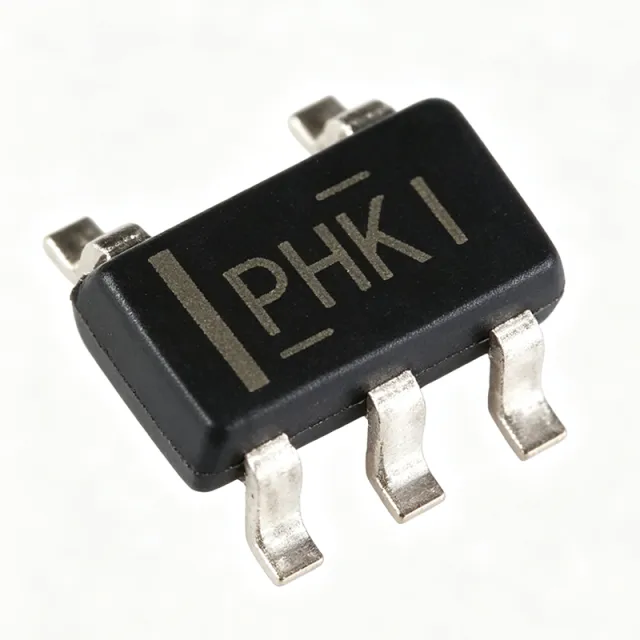
TPS62200DBVR - 300mA, 95% Buck Converter | Texas Instruments
N.º de pieza: TPS62200DBVR ✓ Activo| Cant. | Precio unitario | Total |
|---|---|---|
| 1 | $1.45 | $1,45 |
| 10 | $1.3 | $13,00 |
| 100 | $1.02 | $102,00 |
| 500 | $0.86 | $430,00 |
| 1.000 | $0.69 | $690,00 |
TPS62200DBVR Descripción general
A synchronous buck converter is a type of switching voltage regulator that replaces the traditional freewheeling diode with an integrated low-side MOSFET. Within the power management IC hierarchy (converter -> switching regulator -> DC-DC converter -> power management IC), synchronous topologies achieve higher efficiency than asynchronous designs because conduction losses on the low-side switch are lower than diode forward-voltage losses, especially at light loads.
Key features include up to 95% efficiency across a wide load range, 1 MHz fixed-frequency PWM operation that permits small external inductors (typically 2.2 uH) and capacitors, a 300 mA output current rating, and input compatibility with 1-cell Li-Ion, 3-cell NiMH/NiCd batteries, and standard 3.3 V or 5 V rails. The TPS6220x family also offers fixed-output voltage options, such as the TPS62205DBVR (2.5 V) and TPS62207DBVR (3.3 V), for BOM simplification.
Technically, the TPS62200 integrates both power MOSFETs, the control loop, and protection features in the 5-pin SOT-23 package. The 1 MHz switching frequency reduces the required inductance and shrinks the total solution size for space-constrained portable designs. The FB pin supports precise output regulation through an external resistor divider, setting VOUT via a standard feedback network.
Typical applications include powering low-voltage DSPs and microcontrollers in portable systems, battery-powered point loads in Li-Ion handheld devices, and local point-of-load conversion from 3.3 V or 5 V rails in industrial and consumer electronics.
Design tip: keep the input and output ceramic capacitors (typically 4.7 uF) close to the VIN and SW pins, and choose the adjustable version only when no fixed-output variant of the TPS6220x family matches your rail voltage.
This page synthesizes distributor pricing, drop-in alternatives, comparison tables, and practical design notes not found in the manufacturer datasheet.
Alternativas directas para TPS62200DBVR — mismo encapsulado, compatible pin a pin. Se excluyen las piezas de otro encapsulado que requieren retrabajo de la PCB.
Herramienta de comparación rápida — seleccione piezas alternativas para compararlas lado a lado:
TPS62205DBVR
✅ Sustitución directa📋 Alternativa de referencia (no en el catálogo)
TPS62207DBVR
✅ Sustitución directa📋 Alternativa de referencia (no en el catálogo)
TPS62201DBVR
✅ Sustitución directa ⚠️ Especificaciones sin verificar📋 Alternativa de referencia (no en el catálogo)
TPS62202DBVR
✅ Sustitución directa ⚠️ Especificaciones sin verificar📋 Alternativa de referencia (no en el catálogo)
TPS62200DBVR Valores máximos y características eléctricas
| Topología | Synchronous Step-Down (Buck) |
| Tipo de salida | Adjustable |
| Rango de tensión de salida | 0.7 V to 6 V |
| Rango de tensión de entrada | 2.5 V to 6 V |
| Corriente de salida máxima | 300 mA |
| Peak Efficiency | 95% |
| Frecuencia de conmutación | 1 MHz (fixed) |
| Control Mode | PWM |
| Encapsulado | SOT-23-5 (SC-74A / SOT-753), DBV |
| Tipo de montaje | Surface Mount |
| Temperatura de funcionamiento | -40C to +85C |
| Battery Compatibility | 1-cell Li-Ion, 3-cell NiMH/NiCd, 3.3 V / 5 V rails |
| Typical Inductor | 2.2 uH |
| Número de salidas | 1 |
| Polarity | Positive |
| Estado RoHS | Compliant |
Configuración de pines de TPS62200DBVR
| Pin 1 | VIN — Input supply voltage, 2.5 V to 6 V |
| Pin 2 | GND — Ground |
| Pin 3 | EN — Enable input (device shutdown when low) |
| Pin 4 | FB — Feedback input for adjustable output divider |
| Pin 5 | SW — Switch node - connect to external inductor |
Aplicaciones típicas
TPS62200DBVR es adecuado para 6 aplicacións: Li-Ion Battery-Powered Portable Devices, Point-of-Load Power for Microcontrollers and DSPs, Industrial 3.3 V / 5 V Rail Local Regulation, IoT and Wireless Sensor Nodes, Consumer Audio Accessories, Handheld Medical and Wearable Instruments.
Li-Ion Battery-Powered Portable Devices
The TPS62200DBVR was explicitly designed for portable systems powered by 1-cell Li-Ion or 3-cell NiMH/NiCd batteries, per the TI datasheet. The 2.5 V to 6 V input range covers the full Li-Ion discharge curve from 4.2 V down to 3.0 V, and the up-to-95% synchronous efficiency extracts maximum runtime at the 50-300 mA load levels typical of handheld electronics. Because switching occurs at a fixed 1 MHz, the external 2.2 uH inductor and 4.7 uF ceramic capacitors stay small enough for slim form factors. Placed directly after the battery protector, it steps the cell voltage down to any adjusted level between 0.7 V and 6 V with no switching-frequency noise within the audio band.
Recomendado
Point-of-Load Power for Microcontrollers and DSPs
Low-voltage DSP and MCU cores need tight, low-noise local rails, and the TPS62200DBVR fits this role with its 300 mA rating and adjustable 0.7 V to 6 V output, allowing core voltages to be set precisely via the FB divider. The integrated synchronous MOSFETs remove the external freewheeling diode, improving light-load efficiency that matters when processors idle between tasks. With 1 MHz fixed-frequency PWM, output ripple is predictable and filter design is straightforward, keeping the 4.7 uF output capacitor small. Decouple VIN and SW per TI's datasheet layout guidance to minimize switching-node radiation near sensitive digital return paths.
Recomendado
Industrial 3.3 V / 5 V Rail Local Regulation
The TI datasheet notes the TPS6220x family is suitable for operation from standard 3.3 V or 5 V rails, making the TPS62200DBVR a compact local regulator for sensor nodes, interface cards, and accessory boards in industrial equipment. Its -40C to +85C operating range matches typical industrial ambient specifications, and the tiny SOT-23-5 footprint lets designers place regulation exactly at the load instead of routing long low-voltage traces that pick up noise. Adjustable output also supports odd voltage rails such as 2.8 V for image sensors or 1.8 V for logic banks, all from a single stocked MPN, simplifying spares management across a product family.
Recomendado
IoT and Wireless Sensor Nodes
Battery-operated IoT nodes combine bursty radio TX currents with very low idle draw, and the TPS62200DBVR's 1 MHz fixed PWM switching keeps output impedance low enough to support 300 mA radio bursts without deep voltage sag. Its 95% peak efficiency and synchronous architecture minimize drain on primary cells, extending node lifetime. The adjustable FB network supports the 1.8 V to 3.3 V rails typical of MCUs, sensors, and RF modules, and the 2.2 uH inductor with 4.7 uF ceramics fits the under-20 mm2 power area common in coin-cell or Li-SOCl2 designs. Keep the switching node away from the antenna feedline to protect RF sensitivity.
Recomendado
Consumer Audio Accessories
Portable audio devices benefit from the TPS62200DBVR because its fixed 1 MHz PWM moves switching residue far above the audible band, simplifying downstream filtering for headphone amplifier and codec rails. The converter supplies up to 300 mA, adequate for codec plus small class-D amplifier combinations, and the 0.7 V to 6 V adjustable output matches low-voltage analog rails. Synchronous operation maintains efficiency across the varying load profile of audio playback, extending playtime from a 1-cell Li-Ion source. Add an LC post-filter or ferrite bead on the output when powering high-sensitivity analog stages to suppress switching ripple below audibility thresholds.
Recomendado
Handheld Medical and Wearable Instruments
Wearable monitors and handheld diagnostic instruments need compact, efficient point-of-load conversion from a small Li-Ion cell, and the TPS62200DBVR addresses this with its 2.5 V to 6 V input acceptance, 95% peak efficiency, and minimal 5-pin SOT-23-5 footprint. The adjustable output supports sensor-excitation rails such as 2.5 V or 3.0 V for biopotential front ends, while the -40C to +85C range covers body-worn and sterilization-adjacent environments. The 1 MHz switching frequency allows tiny magnetics that fit curved wearable PCBs. Follow the datasheet layout recommendations - short SW traces and solid ground - to keep switching noise out of microvolt-level physiological signal chains.
Recomendado
Resumen de productos recomendados
Datos de referencia de ingeniería para TPS62200DBVR — comparación, orientación de diseño e información de cumplimiento.
Guía de selección
Comparación con alternativas
| Parámetro | Este producto | TPS62205DBVR | TPS62207DBVR | TPS62201DBVR | TPS62202DBVR |
|---|---|---|---|---|---|
| Package | SOT-23-5 (DBV) | SOT-23-5 (DBV) - same | SOT-23-5 (DBV) - same | SOT-23-5 (DBV) - same | SOT-23-5 (DBV) - same |
| Brand | Texas Instruments | Texas Instruments | Texas Instruments | Texas Instruments | Texas Instruments |
| Output Voltage | Adjustable 0.7 V to 6 V | Fixed 2.5 V | Fixed 3.3 V | Fixed 1.5 V | Fixed 1.8 V |
| Output Current | 300 mA | 300 mA | 300 mA | 300 mA | 300 mA |
| Peak Efficiency | 95% | 95% | 95% | 95% | 95% |
| Input Voltage Range | 2.5 V to 6 V | 2.5 V to 6 V | 2.5 V to 6 V | 2.5 V to 6 V | 2.5 V to 6 V |
| Switching Frequency | 1 MHz fixed | 1 MHz fixed | 1 MHz fixed | 1 MHz fixed | 1 MHz fixed |
| External FB Divider Needed | Yes (2 resistors) | No (fixed output) | No (fixed output) | No (fixed output) | No (fixed output) |
Diferenciadores clave
- Adjustable output flexibility (frente a TPS62207DBVR)
- Fully integrated synchronous rectification (frente a Asynchronous SOT-23-5 bucks)
- 1 MHz fixed-frequency PWM (frente a Lower-frequency SOT-23-5 alternatives)
Notas de diseño
Place the 4.7 uF input ceramic capacitor within 2-3 mm of the VIN pin and the output capacitor close to the inductor output node. Keep the SW switching-node copper area as small as possible while still carrying 300 mA, and return switch currents to the GND pin through a solid, unbroken ground path. Per TI's TPS6220x datasheet layout guidance, route the FB trace away from the SW node to avoid injecting switching noise into the feedback loop, which can cause output jitter and elevated ripple.
Do not exceed the 6 V absolute input limit when using 5 V-tolerant but unregulated USB or adapter sources with transients. Set the adjustable output via 1%-tolerance FB divider resistors; the reference tolerance adds directly to output error. Do not omit the EN pull-up if the rail must always run - leaving EN floating gives an undefined state. Estimated inductor sizing: at VIN=3.6 V, VOUT=1.8 V, 1 MHz, the typical 2.2 uH value from the datasheet yields peak-to-peak ripple of roughly 220 mA at 300 mA load, so choose an inductor with saturation current comfortably above 400 mA.
Estimated: dissipation at VIN=4.2 V, VOUT=1.8 V, 300 mA load, assuming ~92% efficiency, is about 47 mW; the SOT-23-5 theta_JA of roughly 250-300 C/W (package-dependent, board-mounted) produces only about 12-14 C of junction rise - well within the -40C to +85C rating. Thermal design only becomes a concern if the board has minimal copper and high ambient; still, a modest ground pour under the part keeps margins healthy at full load.
Información de cumplimiento
RoHS and REACH compliant per TI product page and distributor comparison data. Not an AEC-Q100 automotive part; TPS6220x family targets portable/consumer/industrial.







