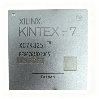
XC7K70T-1FB676I - Kintex-7 FPGA, 300 I/O | AMD
N.º de pieza: XC7K70T-1FB676I ✗ Fin de vida| Cant. | Precio unitario | Total |
|---|---|---|
| 1 | $0.01 | $0,01 |
| 10 | $0.01 | $0,10 |
| 100 | $0.01 | $1,00 |
| 500 | $0.01 | $5,00 |
| 1.000 | $0.01 | $10,00 |
XC7K70T-1FB676I Descripción general
An FPGA is a digital semiconductor whose configurable logic, interconnect, and programmable I/O resources implement hardware functions after manufacturing. In the product hierarchy, the XC7K70T-1FB676I is a Kintex-7 FPGA, then a programmable-logic device, then a semiconductor and integrated circuit. Unlike a fixed-function processor or application-specific IC, its internal architecture can support multiple data paths and interface combinations while retaining upgrade flexibility within the device family.
The Kintex-7 -1 speed grade provides the key ordering indication, while the trailing I identifies the industrial-temperature option in AMD/Xilinx ordering nomenclature. The 676-ball package supports the device's 300 user I/O, making board escape routing and via-in-pad or through-via design significant constraints. Exact logic-cell, memory-block, DSP-slice, clock, voltage, I/O-standard, and performance values were not included in the verified excerpts and therefore require the manufacturer datasheet before design release.
Typical uses include high-speed data acquisition, communications infrastructure, industrial automation, defense-oriented control systems, prototyping, and accelerator logic. A design must assign pins through the AMD toolchain, confirm supported I/O standards and voltage banks, provide compliant clocking and power rails, and complete timing, thermal, signal-integrity, and configuration analysis. The Kintex-7 family is available in -3, -2, -1, -1L, and -2L speed grades, with -3 described in the verified data as having the highest performance.
The principal purchasing issue is supply status rather than generic functionality: distributor results show active sourcing pages, but the target page does not expose an authoritative unit price or target quantity availability. Treat the component as quote/order-on-request until inventory is confirmed. Also verify the exact suffix because XC7K70T-1FBG676I appears in the verified results as a closely related ordering variant, not assume that G or C suffix variants are interchangeable without AMD documentation.
This page combines the verified distributor identity, package and I/O facts, official pinout-resource link, commercial sourcing guidance, and strict replacement criteria. It deliberately avoids unsupported cell counts, pin names, voltage rails, timings, and prices so that engineers can distinguish documented facts from data that still needs manufacturer-level verification.
Alternativas directas para XC7K70T-1FB676I — mismo encapsulado, compatible pin a pin. Se excluyen las piezas de otro encapsulado que requieren retrabajo de la PCB.
Variantes de esta serie
Modelos de la misma serie compatibles directamente con XC7K70T-1FB676I (mismo factor de forma y huella) — difiere en Package, Speed Grade, Block RAM, Configuration Interfaces, Logic Cells.
Herramienta de comparación rápida — seleccione piezas alternativas para compararlas lado a lado:
XC7K70T-1FBG676I
✅ Sustitución directa📋 Alternativa de referencia (no en el catálogo)
XC7K70T-2FB676I
✅ Sustitución directa📋 Alternativa de referencia (no en el catálogo)
XC7K70T-1FBG676C
✅ Sustitución directa✓ En stock
$36.5909 / unidad
Ver hoja de datos →XC7K70T-2FBG676I
✅ Sustitución directa ⚠️ Especificaciones sin verificar✓ En stock
$19 / unidad
Ver hoja de datos →XC7K70T-2FBG676C
✅ Sustitución directa ⚠️ Especificaciones sin verificar📋 Alternativa de referencia (no en el catálogo)
XC7K70T-1FB676I Valores máximos y características eléctricas
| Device Type | Kintex-7 Field Programmable Gate Array (FPGA) |
| Manufacturer | AMD / Xilinx |
| Programmable Logic Type | FPGA |
| User I/O Count | 300 I/O |
| Encapsulado | 676-BBGA, FCBGA |
| Package Ball Count | 676 balls |
| Speed Grade | -1 |
| Temperature Grade Indicator | I |
Guía de configuración de pines de XC7K70T-1FB676I 676 balls
Configuración de pines para XC7K70T-1FB676I (encapsulado 676 balls). Este CI digital incluye GPIO, interfaces de comunicación (UART, SPI, I2C) y pines de alimentación. Consulte la hoja de datos del fabricante para conocer las funciones alternativas de los pines y las opciones de configuración. Esencial para el diseño de sistemas embebidos y el diseño de PCB.

No hay datos detallados de patillaje disponibles para XC7K70T-1FB676I.
Consulte la hoja de datos para ver la configuración completa de patillas.
Aplicaciones típicas
XC7K70T-1FB676I es adecuado para 6 aplicacións: Industrial Control and Automation, High-Speed Data Acquisition, Communications and Network Equipment, Signal Processing and Digital Filters, Aerospace and Defense Control Systems, Test, Measurement, and Instrumentation.
Industrial Control and Automation
The XC7K70T-1FB676I fits industrial control systems that combine parallel machine I/O, high-speed data paths, state-machine logic, and communications in one FPGA. Its 300 user I/O provides substantial board-level connectivity, while the industrial I ordering designation makes it a logical starting point for factory equipment. The device should be used only after confirming its numerical temperature range, supported I/O standards, power rails, and timing in AMD documentation. In a controller, the FPGA can execute deterministic acquisition, motion sequencing, safety interlocks, and protocol conversion concurrently. Its key advantage is reconfigurable hardware: control logic can be revised without changing the surrounding PCB. The 676-ball FCBGA also demands careful escape routing, reference-plane continuity, power delivery, and signal-integrity analysis, so package design is integral to the industrial reliability case.
Recomendado
High-Speed Data Acquisition
The 300-I/O XC7K70T-1FB676I can coordinate parallel ADC capture, digital filtering, packet formatting, and data movement where deterministic hardware pipelines are valuable. Multiple I/O allow source-synchronous or parallel interfaces to coexist, subject to bank, voltage, and timing constraints that are not present in the verified excerpts. Designers should create the ADC interface in the AMD toolchain, verify edge rates and I/O standards, and add data_valid timing checks before hardware release. Compared with an MCU-only implementation, parallel FPGA logic can reduce processor bottleneck and preserve repeatable acquisition timing. The 676-ball package keeps I/O density high but complicates escape routing, so layer planning, return paths, and decoupling must be addressed before fabrication. Exact supported transceiver and acquisition specifications require the manufacturer datasheet.
Recomendado
Communications and Network Equipment
XC7K70T-1FB676I is suitable for communications infrastructure that requires parallel datapaths, packet buffering, custom serialization, and protocol adaptation. The 300 user I/O provide a large pin budget for parallel buses and control signals, but actual line rates depend on the exact I/O standards and timing grades documented by AMD. A network card can assign the FPGA to framing, crossbar, queue, and traffic-shaping functions while external PHYs or optical modules handle physical signaling. The design must constrain clock domains, analyze skew and jitter, and preserve continuous reference planes beneath the dense BGA. Because the verified material does not establish transceiver standards or power-envelope data, engineers should not infer Gen, Gb/s, or protocol compatibility from the Kintex-7 name alone. Complete silicon validation against the chosen PHY and AMD timing models is required.
Recomendado
Signal Processing and Digital Filters
The Kintex-7 FPGA architecture can implement parallel digital filtering, correlation, FFT pipelines, and real-time signal conditioning with deterministic throughput. The XC7K70T-1FB676I’s 300 I/O can connect converters, memory interfaces, clock sources, and control peripherals without relying on a narrow MCU pin set. Logical resource, block-RAM, and DSP counts are not supplied in the verified excerpts, so the first design step is to map the arithmetic pipeline against AMD’s official device tables. Engineers should use synchronous design rules, register pipeline stages, constrain clock uncertainty, and account for package-level skew. A staged conversion interface can reduce fan-out, while dual-clock logic requires explicit asynchronous-control handling. The device offers flexible post-deployment updates, but its large FCBGA demands careful thermal, via, and return-path design to preserve timing margin at operating temperature.
Recomendado
Aerospace and Defense Control Systems
The XC7K70T-1FB676I can serve as a programmable control or acquisition element in aerospace and defense equipment when its documented electrical limits, screening, radiation, and procurement requirements satisfy the program. The I suffix supports selection for an industrial-temperature ordering option, but it is not evidence of radiation hardness, MIL certification, or specific aviation qualification. Engineering teams must distinguish device qualification from system-level design assurance and maintain configuration-control evidence for bitstreams, tool versions, and approved part sourcing. Programmable logic is useful for fault monitoring, sensor fusion interfaces, telemetry packing, and redundant control paths. Nevertheless, the verified excerpts do not provide operating-temperature numbers, life-cycle status, or reliability tests, so release requires official AMD documentation and program-specific screening evidence. Obsolescence and counterfeit mitigation should be addressed early for long-lived systems.
Recomendado
Test, Measurement, and Instrumentation
The XC7K70T-1FB676I is well matched to instrumentation requiring configurable acquisition, pattern generation, timing control, and high pin connectivity. A 300-I/O budget can support multiple parallel channels, though each bank’s voltage and I/O-standard limits must be checked before assignment. The FPGA can generate deterministic stimulus, time digital events, perform online analysis, and transfer results to a host processor. Engineers should separate analog and digital ground-return planning, terminate unused inputs according to device guidance, and validate channel-to-channel skew for timing-critical measurements. Because the target is a large FCBGA, X-ray inspection and assembly yield planning may be necessary, especially where fine pitch or complex escape routing is used. The verified sources identify the package and I/O count but not performance, power, or temperature data, preventing a numerical performance claim.
Recomendado
Resumen de productos recomendados
Datos de referencia de ingeniería para XC7K70T-1FB676I — comparación, orientación de diseño e información de cumplimiento.
Guía de selección
Comparación con alternativas
| Parámetro | Este producto | XC7K70T-1FBG676I | XC7K70T-2FB676I | XC7K70T-1FBG676C | XC7K70T-2FBG676I | XC7K70T-2FBG676C |
|---|---|---|---|---|---|---|
| Brand | AMD | AMD | AMD | AMD | AMD | AMD |
| Package | 676-BBGA FCBGA | 676-BBGA FCBGA | 676-BBGA FCBGA | 676-BBGA FCBGA | 676-BBGA FCBGA | 676-BBGA FCBGA |
| FPGA Family | Kintex-7 | Kintex-7 | Kintex-7 | Kintex-7 | Kintex-7 | Kintex-7 |
| Speed Grade | -1 | -1 | -2 | -1 | -2 | -2 |
| Temperature-Grade Suffix | I | I | I | C | I | C |
| Performance | -1 grade; lower speed designation than -2 | -1 grade | -2 grade; faster than -1 per same-family naming | -1 grade | -2 grade | -2 grade |
Diferenciadores clave
- Exact target ordering designation (frente a XC7K70T-1FBG676I)
- Temperature-grade ordering intent (frente a XC7K70T-1FBG676C)
- Lower speed class can reduce qualification scope (frente a XC7K70T-2FB676I)
Notas de diseño
Treat the 676-ball FCBGA as a constrained-routing design. Start from AMD’s exact package drawing, escape each power, ground, configuration, clock, and user-I/O ball without violating current or via rules, and preserve uninterrupted reference planes under high-speed routes. Validate layer transitions, antipads, via-in-pad construction, solder mask, and assembly process with the selected fabricator; the verified excerpts do not provide a recommended land pattern or via geometry.
Do not infer power-rail values from the -1 suffix. Retrieve the AMD data sheet and determine every core, auxiliary, configuration, and I/O voltage before assigning power pins. Decoupling must follow the manufacturer’s recommended capacitance, voltage, temperature, and placement rules. Verify startup sequencing and configuration behavior with the complete tool-generated power design, since a pin-compatible ordering variant may not have identical power or timing behavior.
Create constraints from actual board and device data, including clock uncertainty, external transceiver timing, I/O standards, bank voltages, and package-ball transitions. For multi-domain designs, use explicit synchronizers or asynchronous FIFOs and avoid relying on combinational paths between unrelated clocks. Run post-route timing and signal-integrity signoff at the intended clock, voltage, and temperature corners; exact values were not present in the supplied search excerpts.
The verified results mix XC7K70T-1FB676I, XC7K70T-1FBG676I, and C or -2 suffix variants. Do not interchange them solely because listings show the same 676-ball package. Confirm the complete AMD ordering code, ball finish, temperature grade, speed grade, pinout, voltage, lifecycle status, and migration guidance. For any proposed substitution, run a formal difference report in the AMD device-selection workflow and obtain manufacturer approval where design assurance requires it.
Información de cumplimiento
The target excerpts do not state target-part compliance. LoveChip describes XC7K70T-1FBG676I as having a lead-free, RoHS-compliant ball finish, but that statement was not assigned to the target or independently verified from AMD documentation.