آیسیهای تقویتکننده
محصولات (1,100+)

TS934ID - 4-Channel 2.7V R-R Micropower Op Amp | STMicroelectronics
The STMicroelectronics TS934ID is a quad, rail-to-rail output, micropower operational amplifier designed for low-voltage signal conditioning and battery-powered systems. It contains four amplifiers in a 14-pin SOIC package, operates from 2.7V to 10V, supports single-supply operation, and is specified for a 100kHz gain-bandwidth product. The device combines a typical 20uA supply current with CMOS inputs, ultra-low input bias current of 1pA, and rail-to-rail output voltage swing. According to the manufacturer datasheet family information, the TS93x series is intended for portable instrumentation, sensor interfaces, and general-purpose analog signal processing. An operational amplifier is an analog integrated circuit that amplifies the voltage difference between its differential inputs while providing high input impedance and low output impedance. The TS934ID belongs to the operational-amplifier hierarchy, which includes general-purpose amplifier ICs, micropower amplifiers, rail-to-rail amplifiers, and CMOS-input analog ICs. Its four integrated channels reduce the number of packages required when several low-frequency signals must be conditioned in the same system. The principal features are the 2.7V minimum supply voltage, 10V maximum supply voltage, 100kHz bandwidth, 0.05V/us slew rate, and approximately 20uA typical supply consumption described for the TS93x family. The output stage can reach 2.9Vpp with a 100kohm load when supplied from 3V, making the amplifier suitable for modest-swing signals in low-voltage systems. CMOS inputs minimize input bias current, which is advantageous when the source impedance is high. The TS934ID is not intended as a high-speed, high-voltage, or precision replacement for every general-purpose quad amplifier. Its 100kHz bandwidth and micropower bias favor portable and instrumentation applications over wideband signal chains. Designers should verify output swing, common-mode range, noise, offset, stability, and load capability against the complete manufacturer datasheet before using it with unusual source impedances, capacitive loads, or rail-to-rail input signals. Typical uses include battery-powered sensor conditioning, portable measurement equipment, industrial transducers, audio and communications interface circuits, and general 3V instrumentation. The 14-SOIC package is suitable for conventional through-hole PCB assembly and automated manufacturing. Because the device is a four-channel amplifier, one package can serve multiple independent amplifier sections in a compact analog front end. A key design consideration is power budgeting. The low supply current supports battery-operated systems, but the output still requires a stable supply and suitable bypass capacitance. The amplifier should be operated within the specified supply range and load conditions, and its output should not be used as a power-stage output. Pin assignments, common-mode behavior, and package details should be taken directly from the STMicroelectronics datasheet and pinout diagram. This page combines verified distributor and manufacturer-linked information, drop-in comparison candidates, pricing fields, application guidance, and practical design notes to support faster component selection and PCB planning.
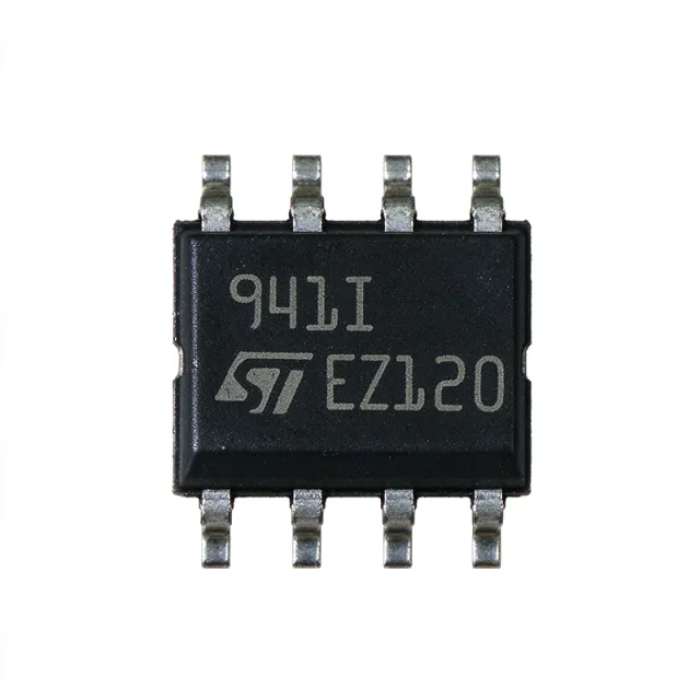
TS941ID - 2.5-10V Rail-to-Rail Op Amp | STMicroelectronics
STMicroelectronics TS941ID is a single-circuit, general-purpose operational amplifier featuring a rail-to-rail output, 2.5 V to 10 V supply operation, and an 8-pin SOIC package. The device belongs to the TS94x micropower operational-amplifier family and is designed for instrumentation, signal buffering, and other low-voltage analog signal-chain applications. Its low-noise operation, high input impedance, and approximately 1 pA input-bias current support accurate handling of high-impedance sources while its rail-to-rail output improves dynamic range near the positive and negative supply rails. An operational amplifier, or op amp, is a high-gain differential amplifier used to amplify, buffer, compare, and filter analog signals. The TS941ID sits within the operational-amplifier hierarchy and operates from a 2.5 V to 10 V supply, making it suitable for battery-powered, industrial-control, test-and-measurement, and portable equipment. Its rail-to-rail output stage allows the output voltage to approach the supply limits more closely than a conventional output stage, although the exact output swing and input common-mode behavior must be checked in the manufacturer datasheet for the selected supply voltage. Key features include a single amplifier configuration, rail-to-rail output, low-noise operation, high input impedance, and very low input-bias current of approximately 1 pA. The 2.5 V minimum supply voltage supports compact, low-energy systems, while the 10 V maximum provides compatibility with common industrial and laboratory supply rails. The manufacturer specifies operation over -40 °C to +85 °C, covering industrial temperature requirements without requiring an automotive-qualified variant. The TS941ID is intended for general-purpose precision signal conditioning rather than as a high-speed communications amplifier. Its micropower-oriented design is valuable when battery current is important, but the precise quiescent-current value should be taken from the manufacturer datasheet. The approximately 1 pA input-bias current is particularly useful with high-impedance sensors because it limits the DC current drawn through the source resistance and helps reduce input-offset errors. Typical applications include sensor-signal conditioning, low-current transimpedance buffering, portable instrumentation, industrial measurement, and general analog signal conditioning. In a transimpedance stage, the TS941ID can be paired with a suitable feedback resistor and compensation capacitor while its low input-bias current reduces bias-current-induced error. In instrumentation, it can buffer inputs before a higher-precision converter or provide gain around sensors whose output range does not use the complete supply span. When designing around the TS941ID, verify input common-mode range, output swing, unity-gain stability, noise, slew rate, and quiescent current against the actual load and supply conditions. Place input, feedback, and decoupling connections for low noise and stable feedback operation, and include adequate output-current margin for capacitive or resistive loads. The 8-pin SOIC footprint is convenient for conventional surface-mount assembly but is not as compact as the smallest QFN packages. This product page consolidates the verified manufacturer information, distributor availability references, family-level alternatives, parameter comparisons, and practical design guidance. It distinguishes confirmed TS941ID data from specifications that still require confirmation from the manufacturer datasheet, helping engineers identify the part faster without presenting unverified values as established facts.

TS944IPT - Quad Rail-to-Rail 1.2µA Op-Amp | STMicroelectronics
The STMicroelectronics TS944IPT is a quad CMOS-input operational amplifier delivering rail-to-rail output swing while consuming only 1.2 µA typical quiescent current per channel, packaged in a 14-pin TSSOP (Tape & Reel). It operates from a single 2.5 V to 10 V supply over the -40 °C to +85 °C industrial temperature range and provides a gain-bandwidth product of 10 kHz, making it ideal for ultra-low-power signal conditioning. An operational amplifier (op-amp) is a high-gain DC-coupled differential amplifier that uses external feedback components to set closed-loop gain, bandwidth, and transfer function. The TS944 belongs to the micropower CMOS op-amp family — a class of linear ICs that prioritize nano- to micro-amp quiescent current draw for battery-powered and energy-harvesting designs. Within the broader semiconductor hierarchy, it sits under: op-amp -> amplifier -> analog IC -> linear IC -> integrated circuit. Key features include four independent op-amp channels in one package, CMOS inputs delivering ultra-low input bias current, rail-to-rail output swing that maximizes dynamic range on low-voltage supplies, and 1.2 µA typical supply current per amplifier that enables years of runtime from small cells. The device is unity-gain stable and supports single-supply operation from 2.5 V to 10 V, simplifying designs that previously needed bipolar ±5 V rails. The TS944 architecture uses a CMOS input stage that achieves very low bias current while the class-AB output stage swings to within millivolts of both supply rails. This combination eliminates the need for input bias-current compensation in high-impedance sensor interfaces and lets designers operate the part directly from a single lithium cell or 3.3 V digital rail without sacrificing headroom. Typical applications include battery-powered sensor signal conditioning, portable medical monitors, IoT edge nodes, active filters, transducer pre-amplifiers, and any micropower analog front end where four amplifiers must fit in a small 14-pin TSSOP footprint. Designers should bypass supplies with 100 nF ceramic capacitors placed within 5 mm of VCC and avoid capacitive loads above 1 nF without an isolation resistor to prevent oscillation.

TS951ID - 3MHz Rail-to-Rail Low-Power Op Amp | STMicroelectronics
STMicroelectronics TS951ID is a single-amplifier, input/output rail-to-rail BiCMOS operational amplifier optimized for 3 V and 5 V operation, with a maximum operating supply voltage of 12 V and operation from the negative rail to the positive rail at input and output. The device is packaged in an 8-pin SOIC and provides approximately 3 MHz gain-bandwidth product, 1 V/µs slew rate, and 80 dB supply-voltage rejection ratio. Its low-power design targets portable instrumentation, sensor interfaces, audio signal conditioning, and general-purpose analog systems. An operational amplifier is an analog integrated circuit that amplifies the voltage difference between its inverting and non-inverting inputs while offering high input impedance, low output impedance, and stable closed-loop behavior when feedback is applied. The TS951 belongs to the operational-amplifier hierarchy, where its BiCMOS input stage combines bipolar transistor performance with CMOS power efficiency. Rail-to-rail input and output operation extends useful signal range toward the supply rails, making the amplifier practical in low-voltage systems that cannot tolerate substantial headroom loss. Key benefits include 3 MHz gain-bandwidth product for modest-frequency signal paths, 1 V/µs slew rate for faster large-signal transitions, and 80 dB supply rejection for reducing supply ripple that could otherwise modulate the amplified signal. The low-power operating approach is useful in portable equipment where energy efficiency and reduced heat generation are priorities. ESD protection rated at 2 kV adds handling robustness, while the compact SOIC-8 package supports conventional surface-mount assembly. The BiCMOS architecture is appropriate for precision and general-purpose analog blocks where low quiescent consumption and rail-to-rail signal handling are more important than high-speed performance. Because this amplifier is intended for low-power rather than high-bandwidth signal chains, applications normally use moderate feedback resistors, explicit gain-setting resistors, and stable output-loading arrangements. Its broad supply capability also permits operation from 3 V and 5 V rails, although each operating point should be checked against the complete electrical limits in the manufacturer datasheet. Typical applications include low-voltage sensor conditioning, buffered analog measurements, portable audio paths, general-purpose instrumentation, and interface buffering around higher-impedance sensors. It can also support low-frequency control or active-filter stages where the 3 MHz gain-bandwidth product provides useful bandwidth margin. In these systems, TS951ID can reduce the loading imposed on the sensor source while maintaining an output signal referenced to the available supply range. Designers should verify input common-mode range, output swing, output-current capability, noise, and stability at the intended frequency before committing the device to a new layout. Decoupling capacitors should be placed close to the supply pins, and sensitive analog inputs should be routed away from switching nodes and high-current return paths. The input and feedback networks must also avoid excessive source resistance or capacitance that could impair stability. This product data combines the verified STMicroelectronics family description, manufacturer datasheet, and distributor listings with practical guidance for package selection, sourcing, and analog layout. It also distinguishes electrically related family members from true drop-in choices and identifies unavailable pricing and lifecycle information rather than presenting unverified commercial figures.
TS952ID - Dual 3MHz Rail-to-Rail Op Amp | STMicroelectronics
STMicroelectronics TS952ID is a dual, input/output rail-to-rail BiCMOS operational amplifier with a 3 MHz gain-bandwidth product, 1 V/us slew rate, and operation from 2.7 V to 12 V in an 8-pin SOIC package. It is optimized and specified for both 3 V and 5 V supply rails, making it suitable for low-voltage analog systems that require an amplifier to approach its supply limits at the input and output. An operational amplifier, or op amp, is a high-gain analog building block used in amplification, buffering, filtering, sensing, and feedback-control circuits. The TS952 belongs to the rail-to-rail op-amp category within the broader amplifier IC and signal-chain hierarchy. Rail-to-rail input and output behavior allows signals near either supply rail to be processed with less conventional headroom loss than a fixed-input amplifier. The TS952ID provides two amplifier circuits, a 3 MHz bandwidth, and a 1 V/us slew rate. According to the STMicroelectronics TS952 product-page data, the device is optimized for 3 V and 5 V operation. Other identified features include an 80 dB supply-voltage rejection ratio, 2 kV ESD protection, and low-power operation. These characteristics make the part applicable to low-voltage sensor conditioning, portable instrumentation, audio input stages, and general-purpose analog signal processing. The BiCMOS architecture combines bipolar input-stage behavior with CMOS output circuitry and is intended to balance low-voltage operation, amplifier performance, and power efficiency. Because the TS952 is a dual device, two independent amplifier channels can share one package. The 8-pin SOIC outline also supports conventional surface-mount assembly, although final stability, bandwidth, and output-current behavior must be evaluated at the intended supply voltage and load. Typical uses include battery-powered sensor interfaces, buffered analog inputs, portable measurement systems, audio preamplification, and low-voltage control loops. At 3 V, the device is aligned with compact battery-operated systems; at 5 V, it provides additional signal range for industrial and consumer analog circuits. The 3 MHz bandwidth is sufficient for many general-purpose conditioning stages but is not intended for high-speed video or precision wideband instrumentation without further analysis. When designing around the TS952ID, verify input and output common-mode limits, output swing, load capability, noise, offset, and stability for the selected supply voltage. Decoupling capacitors should be placed close to the supply pins, and sensitive input traces should remain short and away from switching nodes. Feedback components should follow the manufacturer recommendations because gain-bandwidth, input capacitance, and capacitive loading can affect closed-loop behavior. This product record combines the verified STMicroelectronics family description, distributor package information, operating range, bandwidth, slew rate, rejection, and ESD information with practical selection guidance. It also distinguishes verified facts from specifications that still require confirmation from the complete manufacturer datasheet, avoiding unsupported claims about electrical limits or replacement parts.
TS954ID - Quad 3MHz R-to-R Op Amp | STMicroelectronics
The STMicroelectronics TS954ID is a quad rail-to-rail BiCMOS operational amplifier optimized for 3 V and 5 V operation, with a 3 MHz gain-bandwidth product and 1 V/µs slew rate in a 14-pin SOIC package. The four amplifiers support supply voltages from 2.7 V to 12 V and combine low-power operation with low input bias current. An operational amplifier is an analog integrated circuit that amplifies the voltage difference between its non-inverting and inverting inputs. A rail-to-rail output amplifier can approach the supply rails at its output, making it useful when the available signal range is small. The TS954 belongs to the amplifier IC hierarchy, where operational amplifiers are used for signal conditioning, buffering, active filtering, comparisons, and analog sensor interfaces. The TS954 family provides four amplifiers per package, a 3 MHz gain-bandwidth product, and a 1 V/µs slew rate. Its input bias current is 35 nA, while the listed supply current is 950 µA per channel. These characteristics make it suitable for general-purpose signal conditioning operating from 2.7 V to 12 V, including low-voltage analog systems and battery-powered equipment. The device uses a BiCMOS input architecture combining bipolar and CMOS process characteristics. Its rail-to-rail output stage allows useful output swing near the supply limits, while the low 35 nA input bias current reduces current errors when driving high-impedance sources. The 3 MHz bandwidth is adequate for audio-frequency and general instrumentation tasks, whereas applications requiring substantially faster closed-loop settling should use a higher-bandwidth amplifier. Typical uses include low-level sensor amplification, active analog filters, audio signal conditioning, instrumentation, and four-channel buffering. The SOIC-14 package permits conventional surface-mount assembly and provides one amplifier per two package pins. Its quad configuration can also reduce board area compared with four separate single or dual amplifier packages when all four channels are required. Designers should verify the required output swing, load impedance, input common-mode range, noise performance, and stability against the manufacturer datasheet before finalizing a circuit. Decoupling capacitors should be placed close to the supply pins, and unused amplifier inputs should be biased according to the manufacturer recommendations so that input and output stages remain in their intended operating regions. This page consolidates verified manufacturer and distributor information for the TS954ID, including the 3 MHz bandwidth, 1 V/µs slew rate, 2.7 V to 12 V supply range, 14-pin SOIC format, sourcing links, and the engineering trade-offs that distinguish a low-power quad amplifier from faster or more specialized alternatives.
TS971ID - 12MHz Low-Noise Rail-to-Rail Op Amp | STMicroelectronics
The STMicroelectronics TS971ID is a single, rail-to-rail output operational amplifier with 12 MHz gain-bandwidth product, 4 V/µs slew rate, 4 nV/√Hz input-noise density, and 0.003% ultra-low distortion. The device operates from 2.7 V to 10 V and is supplied in an 8-pin SOIC package. Its combination of low noise, high gain bandwidth, rail-to-rail output swing, and wide supply range makes it suitable for portable audio, instrumentation, sensor conditioning, and general-purpose signal-processing circuits. An operational amplifier is an analog integrated circuit that amplifies the difference between two input voltages. The TS971ID belongs to the operational-amplifier hierarchy within analog and mixed-signal ICs. Rail-to-rail output means the output can swing close to either supply rail, improving usable output range in low-voltage systems. The single-amplifier configuration also keeps the package compact for cost-sensitive designs requiring one precision analog channel. The principal performance features include 12 MHz gain bandwidth and a 4 V/µs slew rate, allowing the amplifier to process relatively fast signals without excessive settling limitations. Input-noise density is specified at 4 nV/√Hz, and the listed distortion is 0.003%. According to the STMicroelectronics product family information, TS97x devices can operate with supply voltages as low as ±1.35 V and are intended for portable and battery-powered equipment. The TS971ID combines rail-to-rail output operation with low-noise and low-distortion behavior. ESD protection is listed at 2 kV, while latch-up immunity is identified as Class A. These characteristics are particularly useful when a circuit must preserve small-signal information while operating from a constrained supply. The amplifier's 2.7 V to 10 V operating range supports conventional 3.3 V, 5 V, and up-to-10 V system rails. Typical uses include microphone and line-level audio preamplification, portable measurement equipment, low-level sensor interfaces, active filters, and buffered sensor outputs. In an audio preamplifier, the 4 nV/√Hz noise density helps limit the amplifier's contribution to the system noise floor. In instrumentation, the 12 MHz bandwidth provides useful signal range, while the 0.003% distortion specification supports high-fidelity signal paths. When designing a TS971ID circuit, verify the input and output common-mode limits, operating-voltage range, output-current capability, and stability requirements against the manufacturer datasheet. Place input, output, and compensation-network components close to the device, and use a suitable output-load arrangement. Because the verified search results do not provide a public price or a complete manufacturer pin table, those details are not inferred here.
TS972ID - 12 MHz Dual Rail-to-Rail Low-Noise Op Amp | STMicroelectronics
STMicroelectronics TS972ID is a dual, output rail-to-rail, very-low-noise operational amplifier with 12 MHz gain-bandwidth product, 4 V/us slew rate, and operation from 2.7 V to 10 V in an 8-pin SOIC package. Its principal characteristics are 4 nV/Hz noise density, 0.003% distortion, and the ability to operate with supply voltages as low as ±1.35 V. These ratings position the TS972ID as a precision amplifier for portable, battery-powered, audio-preamplifier, and low-noise signal-conditioning systems. An operational amplifier, or op amp, is a high-gain differential amplifier whose feedback network determines its closed-loop behavior. Within the integrated-circuit hierarchy, the TS972ID belongs to the operational-amplifier class, amplifier IC category, and broader analog and mixed-signal semiconductor family. Rail-to-rail output capability lets its output approach the supply rails more closely than a conventional amplifier, improving usable output swing in compact low-voltage systems. The TS972ID combines three defining benefits: 12 MHz gain-bandwidth product for moderate-frequency amplification, 4 V/us slew rate for faster signal transitions, and 4 nV/Hz input-voltage noise for low-noise operation. A 0.003% distortion figure further supports high-fidelity signal paths. The dual configuration provides two amplifiers in one 8-pin SOIC, reducing board area compared with two separate single-channel packages. Its low-voltage operating range and rail-to-rail output architecture suit systems that cannot tolerate the headroom required by conventional amplifiers. The 2.7 V to 10 V supply specification permits operation from a single 3.3 V rail, dual ±2.5 V rails, or other compatible supplies. The manufacturer description specifically identifies portable and battery-powered equipment as suitable markets, while the noise and distortion specifications make audio preamplification a natural fit. Typical uses include portable audio preamplifiers, low-noise sensor conditioning, microphone stages, active filters, and buffered sensor outputs. Two amplifiers in one package can implement dual signal channels, instrumentation front ends, or complementary gain stages when their independent inputs and outputs are required. Care is still necessary when driving capacitive loads, observing output-current limits, and controlling stability around the amplifier and feedback network. The primary design consideration is stable implementation of the intended gain. Input and feedback resistances should be selected consistently with the 12 MHz bandwidth and noise target, while board layout should minimize parasitic capacitance and feedback-loop coupling. Decoupling capacitors should be placed close to the supply pins, and unused amplifier channels should be configured according to the manufacturer guidance rather than left floating. This page consolidates the verified TS972ID operating limits, source references, and same-family alternatives with practical selection and layout guidance. It distinguishes documented facts from parameters requiring confirmation, making the result more useful for PCB compatibility reviews, sourcing, and amplifier design decisions.
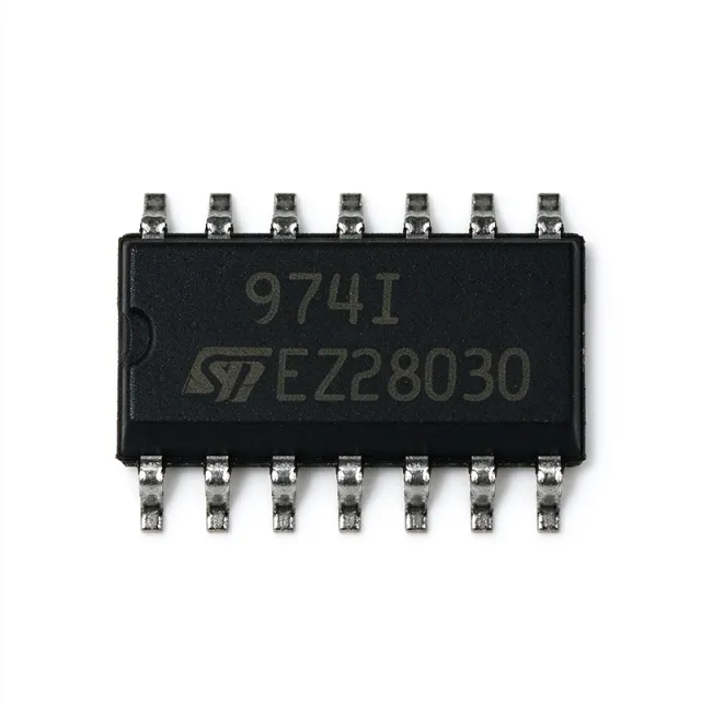
TS974ID - 12 MHz Low-Noise Rail-to-Rail Op Amp | STMicroelectronics
The STMicroelectronics TS974ID is a quad operational amplifier with four rail-to-rail output stages, 12 MHz gain-bandwidth product, 4 V/µs slew rate, and 4 nV/√Hz noise density in a 14-pin SOIC package. It operates from 2.7 V to 10 V, including split-supply operation as low as ±1.35 V, and is intended for portable, battery-powered, audio, sensor, and general-purpose signal-conditioning systems. An operational amplifier is an analog integrated circuit that uses high-gain differential feedback to amplify small voltage signals. The TS974ID belongs to the TS97x family of low-noise, low-distortion amplifiers. Within the broader semiconductor hierarchy, an operational amplifier is an analog amplifier IC, a linear signal-processing component, and ultimately part of a power-management and signal-chain ecosystem. Its four amplifiers combine rail-to-rail output swing with a 12 MHz bandwidth and 4 V/µs slew rate. The stated 4 nV/√Hz noise density supports low-noise signal acquisition, while the specified 0.003% distortion improves linearity in audio and precision analog circuits. A supply range of 2.7 V to 10 V permits operation from a single 3.3 V or 5 V rail or from a split supply as low as ±1.35 V. The TS97x architecture is designed for low-noise and low-distortion performance, with particular suitability for portable and battery-supplied equipment. The quad configuration provides four amplifiers in one 14-pin SOIC package, reducing board area when multiple analog channels require similar electrical performance. Its 12 MHz bandwidth is substantially higher than that required for many slow sensor-conditioning channels, allowing designers to preserve signal fidelity over a wider frequency range. Typical applications include audio preamplification, microphone and sensor conditioning, portable instrumentation, active filtering, data acquisition, and low-voltage embedded systems. The TS974ID is especially useful when several channels must process signals without adding a separate amplifier package for every stage. In audio systems, its low noise and low distortion support cleaner preamplifier operation; in sensors, the rail-to-rail output can improve usable dynamic range on low-voltage supplies. When designing around the TS974ID, account for input common-mode range, output swing, stability with the selected feedback network, and noise bandwidth. Decoupling capacitors should be placed close to the supply pins, while analog input and feedback paths should be kept short and away from switching nodes. Stable feedback components and suitable output loading are important when exploiting the device's 12 MHz bandwidth. This product record consolidates verified manufacturer-family characteristics, distributor availability, package information, and practical application guidance. It also identifies the missing pricing, pin-level, environmental, and qualification details explicitly rather than estimating them, allowing engineers to compare the TS974ID against other low-noise rail-to-rail quad amplifiers before committing to a design.

TSV524IQ4T - Quad 1.15MHz CMOS Op-Amp, RRIO | STMicroelectronics
The STMicroelectronics TSV524IQ4T is a quad CMOS operational amplifier that delivers a 1.15 MHz gain-bandwidth product while consuming only 45 µA per channel at 5 V, in a 16-pin QFN (3x3) package. It operates from a single 2.7 V to 5.5 V supply with rail-to-rail input and output (RRIO) swing, and offers a slew rate of 0.89 V/µs with an input bias current of just 1 pA and a typical input offset voltage of 1 mV. What is a CMOS operational amplifier? A CMOS op-amp is a type of analog integrated circuit that uses complementary metal-oxide-semiconductor transistors in its input and gain stages. Compared to bipolar op-amps, CMOS op-amps typically offer higher input impedance, lower input bias current, and lower quiescent power consumption, making them well-suited for battery-powered and high-impedance sensor interfaces. The TSV524IQ4T sits in the broader taxonomy: operational amplifier -> amplifier IC -> analog IC -> semiconductor. Its RRIO capability means the output can swing within millivolts of both supply rails, maximizing dynamic range in low-voltage single-supply systems. Key features include the high merit factor (1.15 MHz GBW for only 45 µA supply current), 1 pA typical input bias current that simplifies high-impedance sensor signal chains, 100 pF capacitive load drive capability, and the tiny 3x3 mm QFN-16 footprint that enables dense multi-channel designs. An exposed pad (EP) on the package provides a low thermal-resistance path to the PCB, useful when several channels drive continuous loads. Architecturally, the TSV524IQ4T uses a CMOS input stage with rail-to-rail input common-mode range achieved through complementary N/P differential pairs. The output stage is a class-AB CMOS topology that delivers rail-to-rail output swing. This design optimizes the speed-to-power ratio for applications where low quiescent current matters more than raw bandwidth. Typical applications include battery-powered sensor signal conditioning, portable instrumentation, active filters, transducer interfaces, and current-sensing amplifiers. The wide supply range and RRIO capability make it a strong fit for single-cell Li-ion (3.0-4.2 V) and 3.3 V system designs. When designing with this device, note that the QFN-16 package requires careful PCB layout - the exposed thermal pad must be soldered to a sufficiently large copper area to meet the published thermal resistance and to maintain mechanical reliability. Decouple each supply pin with a 100 nF ceramic capacitor placed as close to the IC as possible. This page synthesizes distributor pricing, verified pin-to-pin drop-in alternatives, and PCB/thermal design guidance for the TSV524IQ4T that complements the manufacturer datasheet.
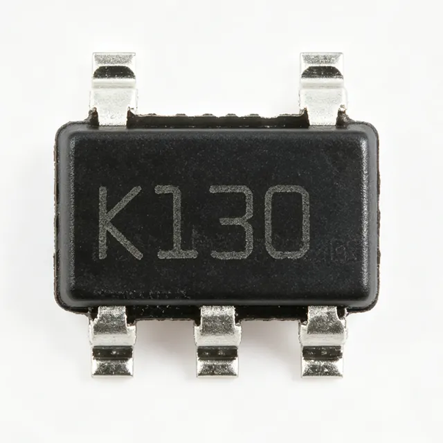
TSV991ILT - 20MHz Rail-to-Rail Op Amp | STMicroelectronics
The STMicroelectronics TSV991ILT is a single, high-speed, rail-to-rail input/output operational amplifier offering a gain-bandwidth product of 20 MHz and a slew rate of 10 V/µs. It operates from a supply voltage range of 2.5 V to 5.5 V, making it suitable for battery-powered and low-voltage applications. The device is available in the compact SOT-23-5 package, ideal for space-constrained designs. An operational amplifier (op-amp) is a high-gain voltage amplifier with differential inputs and a single-ended output. It is a fundamental building block in analog electronics, used in signal conditioning, filtering, and amplification. The TSV991ILT belongs to the family of general-purpose op-amps, which are characterized by their versatility and ease of use. In the hierarchy of analog components, op-amps are part of the broader category of linear integrated circuits, which also includes comparators and voltage regulators. Key features of the TSV991ILT include rail-to-rail input and output stages, which maximize the dynamic range in low-voltage applications. The device also features a low input offset voltage of 1.5 mV (max) and a low input bias current of 1 pA (typ), ensuring high accuracy in precision circuits. The 20 MHz bandwidth and 10 V/µs slew rate enable the amplifier to handle high-frequency signals, making it suitable for video and communication applications. The TSV991ILT is built on STMicroelectronics' advanced BiCMOS process, which combines the benefits of bipolar and CMOS technologies. This process achieves a good balance between speed, power consumption, and noise performance. The amplifier's quiescent current is typically 1.1 mA, providing a favorable trade-off between speed and power efficiency for battery-operated devices. Typical applications include active filters, signal conditioning, portable instrumentation, and audio processing. The rail-to-rail output capability allows the amplifier to drive ADC inputs directly, maximizing the usable input range. In sensor interfaces, the low input bias current minimizes errors when interfacing with high-impedance sensors. When designing with the TSV991ILT, ensure proper power supply decoupling with a 0.1 µF ceramic capacitor placed close to the VCC pin. The input common-mode voltage range extends beyond the supply rails, but care should be taken to avoid exceeding the absolute maximum ratings. The output can swing within 50 mV of the rails, which is beneficial for single-supply operation. This page synthesizes distributor pricing, drop-in alternatives, and practical design notes not found in the STMicroelectronics datasheet, providing a comprehensive resource for engineers evaluating the TSV991ILT.

TSX9292IST - 16MHz RR 16V CMOS Op-Amp, Dual | STMicroelectronics
The STMicroelectronics TSX9292IST is a dual operational amplifier featuring 16 MHz gain-bandwidth product, 27 V/µs slew rate, and 0.0003 % THD+N, housed in an 8-pin MiniSO (Mini Small Outline) package. It operates from a single 4 V to 16 V supply and provides rail-to-rail input and output swing, making it suitable for low-voltage, single-supply, and high-fidelity signal-chain designs. The two on-chip amplifiers are decompensated and stable for gains greater than +2 (or inverting gains less than -1), and each channel draws a typical 2.8 mA quiescent current. A CMOS operational amplifier (op-amp) is a high-gain DC-coupled differential amplifier built on a CMOS process. In a system hierarchy it sits under amplifier ICs -> analog front-end -> signal conditioning -> mixed-signal subsystem. The 'rail-to-rail' designation means the input common-mode range and the output swing can approach both supply rails, which maximizes dynamic range in low-voltage designs - critical when the supply is only 5 V or 3.3 V and every millivolt of headroom counts. Key features include 16 MHz GBP, 27 V/µs slew rate, 0.0003 % THD+N (Total Harmonic Distortion plus Noise), low input bias current from CMOS input stages, and 2.8 mA per-channel quiescent current. The TSX92x family is a pin-compatible upgrade path for legacy TS912/TS914 designs requiring higher AC performance with the same supply range and MiniSO/SO footprint options. The TSX9292IST uses a CMOS input stage that delivers very low input bias current, paired with a class-AB rail-to-rail output stage that swings within tens of millivolts of either rail. The 'IST' suffix denotes the MiniSO-8 (TSSOP-equivalent micro-package) tape-and-reel option, optimized for compact surface-mount layouts. Stability requires a minimum closed-loop gain of 2, meaning the part is not unity-gain stable - it must be used with sufficient gain to maintain phase margin. Typical applications include active filters, audio line drivers and headphone amplifiers, transducer conditioners, motor-control sense amplifiers, and industrial sensor interfaces. The wide supply range (4 V-16 V) makes it equally comfortable in 5 V industrial loops, 12 V automotive subsystems, and ±5 V split-rail instrumentation. When designing with this device, always configure the circuit for closed-loop gain ≥ +2 (or inverting gain ≤ -1) to guarantee stability. Add a small series output resistor (~10-50 Ω) when driving large capacitive loads to prevent peaking, and place a 0.1 µF decoupling capacitor close to each supply pin. Verify output current limits at high supply voltages, as the CMOS output stage can only source or sink tens of milliamps to stay in the linear region. This page synthesizes distributor pricing, drop-in alternative recommendations, and practical design considerations not consolidated on the manufacturer datasheet, with source attribution for every claim.
WM9001GEFL - 1W Class AB/D Speaker Driver | Cirrus Logic
The Cirrus Logic WM9001GEFL is a 1 W mono dual-mode Class AB and Class D speaker driver packaged in a 16-pin QFN with an exposed pad. The distributor data identifies it as an audio amplifier IC with a 1 W output rating, Class AB and Class D operating modes, and a compact 3 x 3 mm QFN package. These characteristics place it in the speaker-driver hierarchy of audio amplifier ICs used to drive small electrodynamic transducers. A speaker-driver amplifier is an integrated circuit that accepts an analog audio signal and delivers enough current and voltage to move a miniature speaker cone. The dual-mode architecture gives a system designer the option to select Class AB behavior for linear output or Class D behavior for higher conversion efficiency. The WM9001GEFL is therefore positioned for compact audio products where speaker output, board area, and energy consumption must be balanced. The WM9001GEFL's principal verified specifications are its 1 W output capability, single-channel mono configuration, support for both Class AB and Class D amplification, and 16-QFN package with an exposed pad. The exposed pad supports heat transfer from the IC into the printed circuit board. Because no verified voltage, current, frequency-response, distortion, thermal-resistance, or shutdown information was supplied, those values must be confirmed in the manufacturer datasheet before final design release. Technically, this device belongs to the integrated-circuit amplifier family and more specifically to speaker-driver audio ICs. Its 3 x 3 mm QFN package supports high-density PCB layouts but demands careful control of exposed-pad soldering, copper thermal paths, and acoustic-mechanical layout. Class AB and Class D modes can also differ in EMI behavior and power efficiency, so mode selection should be based on the complete analog path, speaker impedance, and enclosure conditions rather than package size alone. Typical uses include portable-device speakers, compact consumer-audio products, personal-audio accessories, small embedded audio systems, and accessory modules requiring a mono 1 W drive stage. In these applications, the device can sit near the speaker connector to shorten the high-current output path, reduce load-related board losses, and simplify the analog architecture. Designers should still validate output power at the intended speaker impedance and frequency range. The primary design consideration is thermal management. Although the package includes an exposed pad, continuous Class AB output near the 1 W rating can dissipate more power than Class D operation. The pad should be connected to a suitable ground plane and thermal copper area, while input, feedback, and output routing should avoid the loudspeaker return path. Decoupling and output-filter values must come from the manufacturer application guidance. This product record consolidates verified distributor inventory, package information, source links, engineering caveats, and selection guidance that are not consolidated on a typical distributor listing. Where the supplied evidence does not establish a parameter or a true pin-compatible substitute, the record explicitly marks the gap rather than presenting an unsupported value.

WM9094ECS/R - 2W Mono Class D/AB Amplifier | Cirrus Logic
Cirrus Logic WM9094ECS/R is a 1-channel mono audio amplifier IC delivering up to 2 W into a 4-ohm load, with both Class D and Class AB operation in a 20-WCSP package measuring 2.53 mm by 2.07 mm. The device operates from a 2.7 V to 5.5 V supply and is intended for compact low-power audio systems. An audio amplifier is an integrated circuit that converts an input audio signal into sufficient output power to drive a loudspeaker or other transducer. Class AB amplifiers provide linear operation with comparatively continuous output current, while Class D amplifiers switch the output stage to improve power-conversion efficiency. The WM9094ECS/R supports both operating modes, giving designers flexibility according to their efficiency, distortion, and thermal requirements. Key features include Class D and Class AB output capability, a 2 W maximum output-power rating into 4 ohms, integrated depop circuitry, integrated thermal protection, and a surface-mount 20-WCSP package. The 2.7 V minimum supply voltage supports portable and space-constrained equipment, while the 5.5 V maximum supply voltage accommodates common low-voltage power rails. The WM9094ECS/R is identified as a mono, one-channel amplifier rather than a multi-channel power amplifier. Its compact 2.53 mm by 2.07 mm package can reduce board area in mobile accessories, personal-audio products, and other integrated audio equipment. The manufacturer and distributor listings identify it as an ultra-low-power audio subsystem and list the part as obsolete. Typical applications include compact speaker systems, portable audio accessories, and low-voltage embedded products where a single amplified channel is sufficient. System-level implementation must account for the 2.7 V to 5.5 V supply range, speaker impedance, output power, thermal conditions, and the small-area land-pattern requirements of the 20-WCSP package. The principal design consideration is the obsolete lifecycle status. Designers should verify availability, source quality, and long-term supply before committing to a new production design. For a new design with obsolete risk, engineers may need to qualify an alternative rather than assume that any Class D or Class AB amplifier is pin compatible. This page consolidates the verified distributor specifications, lifecycle information, package details, sourcing links, practical application guidance, and an explicit assessment of replacement availability. It also separates documented parameters from missing technical data instead of presenting unverified electrical characteristics as guaranteed specifications.