محصولات (46,000+)

SN74AVC4T234 - 4-Bit Dual-Supply Level Translator | TI
SN74AVC4T234

SN74AVC4T234 - 4-Bit Dual-Supply Level Translator | TI

The SN74AVC4T234 is a 4-bit, dual-supply noninverting voltage level translation device from Texas Instruments. It is designed to facilitate asynchronous communication between B-port inputs and A-port outputs, with each port referenced to its own supply rail (VCCB and VCCA). The device operates across a wide VCC range of 0.9 V to 3.6 V, making it suitable for low-power, battery-powered portable applications where both static and dynamic power consumption must be minimized. A voltage level translator, also known as a level shifter, is a type of logic IC that allows digital signals to be transferred between circuits operating at different voltage levels. It is essential in mixed-voltage systems, such as interfacing a 1.8V microcontroller with a 3.3V peripheral. The SN74AVC4T234 belongs to the AVC family of advanced very-low-voltage CMOS logic, which is optimized for high-speed operation with minimal power consumption. Key features of the SN74AVC4T234 include its dual-supply configuration, which provides independent power rails for each port, ensuring proper voltage translation without signal distortion. The device maintains excellent signal integrity across the entire VCC range, and its low static and dynamic power consumption extends battery life in portable devices. The noninverting architecture preserves signal polarity, simplifying system design. Technically, the SN74AVC4T234 uses a configurable voltage translation scheme that automatically adjusts output drive strength based on the supply voltage. This ensures reliable operation even with varying supply levels. The device is available in a small package, making it ideal for space-constrained applications. Its propagation delay is minimal, supporting high-speed data transfer. Typical applications include interfacing between different voltage domains in smartphones, tablets, and other portable electronics, as well as in industrial control systems where sensors and microcontrollers operate at different voltages. The device is also used in networking equipment and data communication systems. When designing with the SN74AVC4T234, ensure that both VCCA and VCCB are powered and within the specified range. Proper decoupling capacitors should be placed near the supply pins to maintain stable operation. The device supports bidirectional level translation, but the direction is controlled by the DIR pin, which must be set correctly for the desired data flow.

RFQ تماس
SN74AVC4T245PWR - 4-Bit Dual-Supply Level Shifter | TI
SN74AVC4T245PWR

SN74AVC4T245PWR - 4-Bit Dual-Supply Level Shifter | TI

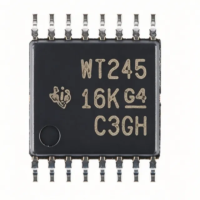
The Texas Instruments SN74AVC4T245PWR is a 4-bit dual-supply bus transceiver with configurable voltage translation and 3-state outputs, supplied in a 16-pin TSSOP (PW) package. It operates from two independent supply rails, VCCA and VCCB, each ranging from 0.8V to 3.6V, enabling bidirectional level shifting between mixed voltage domains such as 1.2V, 1.5V, 1.8V, 2.5V, and 3.3V. A bus transceiver is a digital integrated circuit that transfers data bidirectionally between two buses, using direction-control and output-enable inputs plus 3-state outputs so multiple devices can share a common bus. The SN74AVC4T245 belongs to the voltage translator (level shifter) family within the broader logic IC and interface IC hierarchy, and it is essential in mixed-voltage systems where MCUs, FPGAs, sensors, and memory operate at different logic levels. Key features include configurable voltage translation on both ports, control inputs (1DIR, 2DIR, 1OE, 2OE) referenced to VCCA for simplified control logic, and Ioff partial-power-down circuitry that disables outputs and prevents damaging backflow current when either rail is at GND. A VCC isolation feature places all I/O in high-impedance if either supply is absent. Technically, the device supports asynchronous communication between two data buses at data rates up to 380 Mbps with a typical propagation delay around 2.5 ns, suiting high-speed SPI, parallel bus, and GPIO interfaces. The TSSOP-16 package has a 4.4mm body width and 0.65mm pin pitch for space-constrained PCBs. Typical applications include level shifting for SPI, UART, I2C-adjacent GPIO expansion, and FPGA or ASIC interconnects in industrial control, portable battery-powered electronics, and automotive modules where multiple voltage domains coexist. Design tip: keep the DIR and OE pins driven from VCCA-domain logic and place 0.1uF decoupling capacitors close to both VCCA and VCCB pins; avoid bus contention by sequencing direction changes with a brief high-impedance interval.

RFQ تماس
SN74AVC4T245PWR - 4-Bit Dual-Supply Level Shifter | TI
SN74AVC4T245PWR

SN74AVC4T245PWR - 4-Bit Dual-Supply Level Shifter | TI

The Texas Instruments SN74AVC4T245PWR is a 4-bit dual-supply bus transceiver with configurable voltage translation and 3-state outputs, supplied in a 16-pin TSSOP (PW) package. It operates from two independent supply rails, VCCA and VCCB, each ranging from 0.8V to 3.6V, enabling bidirectional level shifting between mixed voltage domains such as 1.2V, 1.5V, 1.8V, 2.5V, and 3.3V. A bus transceiver is a digital integrated circuit that transfers data bidirectionally between two buses, using direction-control and output-enable inputs plus 3-state outputs so multiple devices can share a common bus. The SN74AVC4T245 belongs to the voltage translator (level shifter) family within the broader logic IC and interface IC hierarchy, and it is essential in mixed-voltage systems where MCUs, FPGAs, sensors, and memory operate at different logic levels. Key features include configurable voltage translation on both ports, control inputs (1DIR, 2DIR, 1OE, 2OE) referenced to VCCA for simplified control logic, and Ioff partial-power-down circuitry that disables outputs and prevents damaging backflow current when either rail is at GND. A VCC isolation feature places all I/O in high-impedance if either supply is absent. Technically, the device supports asynchronous communication between two data buses at data rates up to 380 Mbps with a typical propagation delay around 2.5 ns, suiting high-speed SPI, parallel bus, and GPIO interfaces. The TSSOP-16 package has a 4.4mm body width and 0.65mm pin pitch for space-constrained PCBs. Typical applications include level shifting for SPI, UART, I2C-adjacent GPIO expansion, and FPGA or ASIC interconnects in industrial control, portable battery-powered electronics, and automotive modules where multiple voltage domains coexist. Design tip: keep the DIR and OE pins driven from VCCA-domain logic and place 0.1uF decoupling capacitors close to both VCCA and VCCB pins; avoid bus contention by sequencing direction changes with a brief high-impedance interval. This page synthesizes distributor pricing, drop-in alternatives, and practical design notes not found in the manufacturer datasheet.

USD $0.38 تماس
SN74AVC8T245DGVR - 8-Bit Dual-Supply Bus Transceiver | TI
SN74AVC8T245DGVR

SN74AVC8T245DGVR - 8-Bit Dual-Supply Bus Transceiver | TI

The Texas Instruments SN74AVC8T245DGVR is an 8-bit dual-supply bus transceiver with configurable voltage-level shifting and 3-state outputs, housed in a 24-pin TVSOP (DGV) package. It supports data translation between two independently configurable voltage rails from 1.2 V to 3.6 V on VCCA and 1.2 V to 3.6 V on VCCB, with direction control via the DIR pin and output enable via the active-low OE pin. The device delivers high-speed signal transmission with typical propagation delay of approximately 2.5 ns at 3.3 V and ±12 mA output drive strength. A dual-supply bus transceiver is a logic IC that bridges two voltage domains in a digital system, allowing a microcontroller or ASIC on one rail (for example 1.8 V) to communicate with peripherals or memory on another rail (for example 3.3 V). The 'dual-supply' architecture uses two independent VCC pins (VCCA and VCCB) so each side of the transceiver references its own rail. Within the broader product taxonomy, this part belongs to the level shifter / voltage translation transceiver family, which sits under interface ICs and ultimately under integrated circuits. Key features of the SN74AVC8T245 include Ioff partial-power-down support for live insertion and hot-swap scenarios, VCC isolation that forces all I/O into high-impedance when either supply is at GND, and bus-hold circuitry on the data I/Os to eliminate the need for external pull-up or pull-down resistors. The DIR pin controls signal direction (A-to-B or B-to-A), and OE disables the outputs when high. The wide 1.2 V to 3.6 V operating range covers all common logic standards including 1.2 V, 1.5 V, 1.8 V, 2.5 V, 3.3 V, and lower-voltage CMOS. Architecturally, the device uses TI's AVC (Advanced Very-low-voltage CMOS) process technology, which combines low static power consumption with high drive strength and fast edge rates. The integrated bus-hold cells use weak feedback transistors to retain the last driven logic state on floating lines, eliminating external bias resistors. Ioff circuitry blocks the internal parasitic diode paths when VCC is removed, so the part can be safely inserted or removed from a powered backplane. Typical applications include level shifting between a 1.8 V host processor and 3.3 V peripherals, I2C or general-purpose GPIO expansion, SD-card or SIM-card interfaces, and translating logic between FPGAs and DDR memory rails. The wide voltage range makes it useful in industrial, consumer, and portable battery-powered designs. When designing with this part, place a 0.1 µF decoupling capacitor on each VCC pin and route the DIR and OE pins directly to a GPIO of the controlling host. Avoid leaving either VCC pin floating; unused VCC must be tied to its corresponding rail or to GND to ensure proper high-impedance behavior. This page synthesizes distributor pricing, drop-in alternatives, and practical design notes that go beyond the manufacturer datasheet, helping engineers select and source the part efficiently.

RFQ تماس
SN74AVCB164245GR - 16-Bit Dual-Supply Level Translator | Texas Instruments
SN74AVCB164245GR

SN74AVCB164245GR - 16-Bit Dual-Supply Level Translator | Texas Instruments

The Texas Instruments SN74AVCB164245GR is a 16-bit dual-supply bus transceiver with configurable voltage translation and 3-state outputs, housed in a 48-pin TSSOP (DGG) package. It supports bidirectional level translation between two supply rails from 1.4 V to 3.6 V on the A-port and 1.4 V to 3.6 V on the B-port, with separate VCCA and VCCB power pins per port group enabling asymmetric voltage domains. A bidirectional level translator (also called a voltage level shifter) is an integrated circuit that safely bridges two subsystems operating at different logic-voltage rails. The SN74AVCB164245 belongs to the widebus transceiver family and provides 16 channels split into two 8-bit groups, each with its own direction-control pin. This device class is essential in mixed-voltage systems where modern processors operate at 1.8 V or 1.2 V while legacy peripherals, memories, or bus interfaces remain at 2.5 V or 3.3 V. Key features include a typical propagation delay of 3.7 ns (VDD = 3.3 V), ±12 mA drive strength per channel, 3.5 ns maximum output skew, and partial-power-down capability through Ioff circuitry that prevents damaging backflow current when the device is unpowered. The DIR inputs set the direction of data flow per 8-bit bank, while the OE pins place outputs in high impedance for bus isolation. The SN74AVCB164245 uses TI's DOC (Dynamic Output Control) circuitry, which dynamically switches output impedance to reduce line-noise transients without external damping components. This active damping eliminates the typical ringing seen on heavily loaded memory buses, which improves signal integrity at high data rates. Typical applications include memory-card interfaces between SoCs and DDR/LPDDR memories, GPIO expansion between low-voltage MCUs and 3.3 V peripherals, FPGA-to-MCU bridge logic in industrial controllers, I2C/SPI/UART bridge isolation, and smartphone baseband-to-application-processor interconnects. The dual-supply design is particularly suited to portable electronics where minimizing both voltage drop and leakage current is critical. When designing with this device, ensure VCCA and VCCB rails are decoupled with 0.1 uF ceramic capacitors placed within 5 mm of the supply pins. The OE and DIR logic thresholds are referenced to their respective supply rails, so control signals must be level-shifted into the appropriate domain. Avoid leaving OE floating; tie through a 10 kohm resistor to the high-side supply rail of the controlling port. This page synthesizes distributor pricing, parametric alternatives, and practical design notes not found in the manufacturer datasheet. Pricing references are stated as of 2026-10-04.

RFQ تماس
SN74AXC4T774BQBR - 4-Bit Dual-Supply Bus Transceiver | Texas Instruments
SN74AXC4T774BQBR

SN74AXC4T774BQBR - 4-Bit Dual-Supply Bus Transceiver | Texas Instruments

The Texas Instruments SN74AXC4T774BQBR is a 4-bit dual-supply bus transceiver with configurable voltage translation, independent direction control inputs, and 3-state outputs, housed in a 16-pin WQFN package (2.5 mm x 3.5 mm). It supports an input voltage range of 0.65 V to 3.6 V on the A-port and 0.65 V to 3.6 V on the B-port, allowing seamless level shifting between any two voltage nodes from 0.65 V up to 3.6 V without external direction-control logic. The SN74AXC4T774 belongs to the bus transceiver / level shifter category (a sub-family of voltage level translators within interface ICs / logic ICs). Level translators are interface ICs that allow digital signals to pass between two parts of a system that operate at different supply voltages. They are an essential building block in mixed-voltage designs where low-voltage processors and ASICs must communicate with legacy 1.8 V, 2.5 V, or 3.3 V peripherals, and they enable designers to maintain backwards compatibility while taking advantage of new low-voltage cores. Key features of the SN74AXC4T774 include a typical data rate of 110 Mbps, 4.4 ns typical propagation delay, partial-power-down support via Ioff, and a control-pin reference (DIR and OE) tied to VCCA for simple GPIO-driven control. The AXC family offers the industry's lowest static power consumption in this class, helping portable and battery-powered designs extend runtime without sacrificing throughput. The internal architecture uses TI's AXC CMOS technology with one-shot edge accelerators that detect rising or falling edges on the I/O pins and briefly speed up the output drivers to achieve high data rates with low dynamic power. The DIR pin determines signal direction, while OE enables a high-impedance output mode for bus isolation. Both A and B ports support 3.6-V tolerant I/O on the lower-voltage side, simplifying board design. Typical applications include I2C / SPI / UART bridging between low-voltage SoCs and 3.3 V peripherals, MIPI / camera-serializer voltage translation, SD-card level shifting, and general-purpose GPIO expansion in industrial controllers, wearables, and portable IoT endpoints. A key design consideration is to always tie the OE pin to VCCA through a pull-up resistor (or to a dedicated GPIO) so that the I/Os enter high-impedance during power-up or power-down, preventing bus contention and back-powering. This page synthesizes distributor pricing, same-brand and cross-brand drop-in alternatives in the WQFN-16 footprint, and practical design notes not collated in the manufacturer datasheet alone.

RFQ تماس
SN74AXC8T245RJWR - 8-Bit Dual-Supply Bus Transceiver | Texas Instruments
SN74AXC8T245RJWR

SN74AXC8T245RJWR - 8-Bit Dual-Supply Bus Transceiver | Texas Instruments

The Texas Instruments SN74AXC8T245RJWR is an 8-bit non-inverting, bidirectional dual-supply bus transceiver with configurable voltage translation and 3-state outputs, housed in a 24-pin UQFN (RJW, 4x2 mm) package. It supports independent power-supply rails on each port from 0.65 V to 3.6 V, output drive current of 12 mA, and is fully specified for partial-power-down applications using Ioff. The device operates over an industrial -40C to +125C temperature range. A bus transceiver is a digital logic IC that bridges two buses operating at different voltage levels, allowing data to flow in either direction while protecting each side from incompatible logic levels. The SN74AXC8T245 belongs to TI's AXC family of voltage-level translators, which sit in the broader hierarchy: level translator -> bus transceiver -> logic IC -> semiconductor. The AXC series extends the older AVC and LVC families to lower supply nodes (0.7 V, 0.8 V, 0.9 V) used in modern ASICs, FPGAs, and processors while remaining backward-compatible with industry-standard 1.8 V, 2.5 V, and 3.3 V nodes. Key features include configurable direction control per direction (DIR pin), an active-low output-enable (OE) input that disables both ports to a high-impedance state, 12 mA balanced output drive strength, and ±24 mA DC latch-up protection. The Ioff circuitry disables the outputs when either VCC rail is powered down, preventing backflow current into a partially powered system - a critical requirement for hot-swap and multi-rail designs. Technical depth: the AXC architecture uses TI's advanced CMOS process with internal edge-rate accelerators that limit output rise/fall times to reduce EMI while preserving sufficient bandwidth for RGMII and similar multi-hundred-MHz interfaces. The dual-rail design means the DIR and OE control pins are always referenced to VCCA, simplifying control logic on the lower-voltage side. Typical applications include RGMII level shifting between an SoC and a PHY, I2C/SPI/UART bridging in mixed-voltage embedded systems, memory-bus isolation, and processor-to-peripheral translation in industrial and consumer designs. The 24-pin UQFN (4x2 mm) footprint keeps board area minimal. Design consideration: always populate both VCCA and VCCB decoupling capacitors (0.1 uF ceramic) within 2 mm of the respective pins, and ensure OE is held low until both rails have ramped to valid levels to avoid bus contention at startup. This page synthesizes distributor pricing, drop-in alternatives, and practical design notes not found in the manufacturer datasheet.

RFQ تماس
SN74BCT574 - Octal D-Type Flip-Flop 3-State | Texas Instruments
SN74BCT574

SN74BCT574 - Octal D-Type Flip-Flop 3-State | Texas Instruments

The Texas Instruments SN74BCT574 is an octal D-type edge-triggered flip-flop with 3-state outputs, built on a state-of-the-art BiCMOS process and designed to drive highly capacitive or relatively low-impedance loads in high-speed bus-oriented systems. It operates from a 4.5 V to 5.5 V supply and is offered in DB (SSOP), DW (SOIC), N (PDIP), and NS (SOP) packages. An octal D-type flip-flop is a digital logic register that stores eight bits of data, capturing the logic level present on each D input at the rising edge of a common clock and presenting it on the corresponding Q outputs. In the broader logic-IC hierarchy, it belongs to the flip-flop and register family of sequential logic, a core building block of microprocessor bus interfaces. Its 3-state outputs can be disabled via an active-low output-enable (OE) pin, allowing multiple devices to share a common data bus without contention. Key features include the BiCMOS design that significantly reduces ICCZ (high-impedance supply current), full parallel access for loading all eight bits on one clock edge, and strong bipolar output drive for heavy capacitive bus loads. According to TI datasheet SCBS074C, the edge-triggered architecture guarantees that data is captured only on the rising clock edge, giving predictable setup and hold behavior in synchronous systems. Technical depth: the BCT (BiCMOS) technology combines TTL-compatible input thresholds with bipolar totem-pole output stages, delivering low dynamic supply current at high clock frequencies and high output current capability, making it superior to pure CMOS ABT/ACT predecessors for heavily loaded 5 V buses. Typical applications include buffer registers, I/O ports, bidirectional bus drivers, working registers in microprocessor systems, memory address/data latching, industrial control, and communication interfaces where reliable latching plus high bus drive are required. Design tip: control OE properly to avoid bus contention (OE low enables outputs, high forces high-Z), decouple VCC close to the pins with 0.1 uF ceramic capacitors, and drive the clock with a clean edge to avoid metastability.

RFQ تماس
SN74CBT16209ADGV - 18-Bit FET Bus-Exchange Switch | Texas Instruments
SN74CBT16209ADGV

SN74CBT16209ADGV - 18-Bit FET Bus-Exchange Switch | Texas Instruments

The Texas Instruments SN74CBT16209ADGV is an 18-bit FET bus-exchange switch from the Widebus family, delivering high-speed TTL-compatible bus switching or exchanging in a 48-pin TVSOP (DGV) package. It functions as a 9 x 2:2 crosspoint/exchange switch capable of data exchange between four signal ports via three data-select (S0, S1, S2) terminals, making it suitable for high-performance digital systems requiring flexible signal routing. Background: a FET bus switch is a digital interface IC that uses MOSFET pass transistors to connect or isolate buses with minimal propagation delay and very low on-state resistance. Unlike analog muxes, FET bus switches are unidirectional signal paths optimized for 5V TTL logic levels. They sit in the hierarchy of digital logic ICs (TTL/CMOS logic -> bus interface -> bus switch -> FET bus-exchange switch), serving as the building blocks for memory interleaving, card-edge bus switching, and bus arbitration in backplane designs. Key specifications include 5V nominal VCC operation, TTL-compatible input levels on the select control pins, low on-state resistance for minimal propagation delay, and an approximate propagation delay of 0.35 ns as listed by distributors. The device provides five switch connection modes between two ports, allowing engineers to route 9-bit data slices between four signal ports. A low rON enables clean high-speed switching without driving large currents through the internal pass-FETs. Architecturally, the SN74CBT16209A uses N-channel MOSFET pass gates driven by TTL-compatible level shifters, with the S0-S2 select lines decoded to one of five switch configurations. The exchange/crosspoint topology (9 x 2:2) means the part can connect any one of two buses on each side of an exchange switch to either of two buses on the opposite side, providing bidirectional bus steering in a single IC. The Widebus footprint integrates all 18 bits in one package to minimize board space. Typical applications include high-speed memory bus switching, board-to-board data routing, server backplanes, bus isolation in hot-swap systems, and graphics-card memory interface multiplexing. The 48-pin TVSOP package is well-suited for high-density card-edge designs where fine-pitch surface-mount parts are required. Design consideration: the SN74CBT16209A requires a clean 5V supply with adequate decoupling (0.1uF ceramic close to VCC pins); unused inputs must be tied to VCC through a pull-up resistor to avoid floating-select states. When migrating between the DGG, DGV, DL, and WD package variants, verify pinout compatibility because the package options differ in pitch (TVSOP vs SSOP vs ceramic flat). Unique value: this page consolidates the SN74CBT16209ADGV datasheet parameters, alternative TVSOP-48 drop-in options, and proven PCB layout tips that go beyond the TI datasheet application notes.

RFQ تماس
SN74CBT3245ADWR - Octal FET Bus Switch 5V SOIC-20 | TI
SN74CBT3245ADWR

SN74CBT3245ADWR - Octal FET Bus Switch 5V SOIC-20 | TI

The Texas Instruments SN74CBT3245ADWR is an octal FET bus switch providing eight bits of high-speed TTL-compatible bus switching in a 20-pin SOIC (DW) package with the standard 245-type pinout. Operating from a 4.5V to 5.5V supply, the device is organized as a single 8-bit switch with one output enable (OE) control input; when OE is low, the switch connects the two 8-bit ports bidirectionally. A FET bus switch is a type of analog switch that uses N-channel MOSFET pass transistors to connect or disconnect signal paths between two ports. Within the signal-routing hierarchy, bus switches sit between logic buffers and analog multiplexers: unlike buffers they add negligible propagation delay, and unlike analog MUXes they are optimized for high-bandwidth digital bus isolation. The SN74CBT3245A belongs to the CBT (CrossBar Technology) family, optimized for low on-state capacitance and high bandwidth. Key features include a low on-state resistance of typically 5 ohms, propagation delay of less than 250 ps, and near-zero added jitter because signals pass through an analog FET path rather than a buffered logic stage. The switch supports bidirectional data flow and 5-V level handling, suited to signal switching rather than power delivery. Technically, the device is fabricated in a CMOS process achieving low static power consumption. The internal FET switch presents a low-capacitance, low-resistance path that minimizes signal distortion, and the 245-type pinout matches industry-standard octal transceiver footprints across SOIC, SSOP, TSSOP, and TVSOP package options. Typical applications include bus isolation in microprocessor systems, hot-swap and power-down isolation on backplanes, memory bus switching, and signal routing in networking and telecommunications equipment where high-speed data buses must be connected or isolated under logic control. A key design consideration: control the OE pin properly to avoid bus contention, and note this part is EOL per TI.com - plan the drop-in alternatives listed on this page for new designs.

RFQ تماس
SN74CBTLV1G125DBVR - 3.3V Single FET Bus Switch SOT-23-5 | TI
SN74CBTLV1G125DBVR

SN74CBTLV1G125DBVR - 3.3V Single FET Bus Switch SOT-23-5 | TI

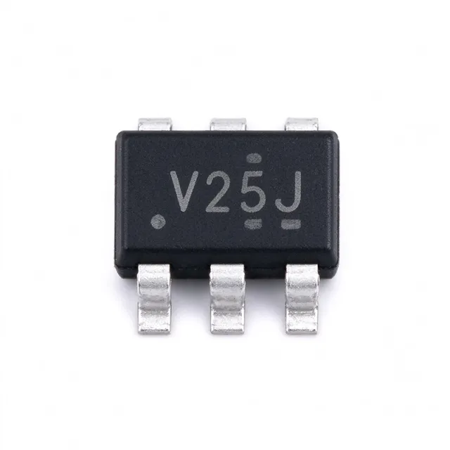
The Texas Instruments SN74CBTLV1G125DBVR is a 3.3-V, single-channel, 1:1 (SPST) FET bus switch housed in a 5-pin SOT-23 (DBV) package. It provides a 5-ohm (typ) on-state resistance rail-to-rail switch path between two ports, with an active-low output enable (OE) input and Ioff support for partial-power-down mode operation. A bus switch (also called a FET switch or pass-gate switch) is a digital building block that replaces mechanical relays and discrete MOSFET switches in CMOS logic designs. The CBTLV family uses parallel n-channel and p-channel MOSFETs to provide a low-resistance bidirectional connection when enabled, achieving propagation delays under 0.25 ns. Bus switches sit within the logic-IC hierarchy as signal switches, above multiplexers and below general-purpose logic gates, and are essential for level shifting, signal multiplexing, and isolating subsystems on shared digital buses. Key features include 5-ohm typ on-resistance (ron) measured at VCC = 3.3 V, rail-to-rail switching on data I/O ports, low quiescent current of 10 uA max, and 5.5 V tolerant I/O when VCC = 0 V thanks to the Ioff isolation. The SN74CBTLV1G125 is one of the smallest 1-channel bus switches available, making it ideal for space-constrained mobile and portable designs where a single high-speed line must be routed or isolated. Architecturally, the device uses a parallel NMOS/PMOS pass gate controlled by a single OE-bar input. When OE-bar is low, both FETs turn on, creating a low-resistance channel between pin A (input) and pin Y (output); when OE-bar is high, the channel opens and the switch enters a high-impedance state. The Ioff circuitry prevents backfeeding through the switch when VCC is removed, eliminating parasitic current paths in partial-power-down or hot-swap scenarios. Typical applications include USB type-C signal routing and protection, I2C/UART bus isolation in battery-powered devices, SD card muxing, GPIO expansion, and reset signal gating in microcontroller-based designs. The SOT-23-5 footprint makes the part convenient for hand-rework on prototype boards. When designing with this device, place a 1 nF to 10 nF decoupling capacitor as close as possible to the VCC pin and observe ESD precautions when handling the small-outline package. Pull-up on OE-bar ensures defined behavior during power-up sequencing in microcontrollers with high-impedance control pins. This page synthesizes distributor pricing, drop-in alternatives, and practical design notes not found in the manufacturer datasheet alone.

USD $0.26 تماس
SN74CBTLV3257PWR - 4-Bit 2:1 FET Mux 5Ω | TI
SN74CBTLV3257PWR

SN74CBTLV3257PWR - 4-Bit 2:1 FET Mux 5Ω | TI

The Texas Instruments SN74CBTLV3257PWR is a low-voltage 4-bit 1-of-2 FET multiplexer/demultiplexer designed for 3.3-V operation. It provides four independent 2:1 (SPDT) analog switch channels in a compact 16-pin TSSOP (PW) package, enabling high-speed signal routing with minimal propagation delay and low ON-state resistance. A multiplexer/demultiplexer is a signal-routing switch that directs one of several inputs to a common output, or vice versa. Within the logic and signal-switching hierarchy, the SN74CBTLV3257 belongs to the CBTLV family of bus (FET) switches, which sit between simple logic gates and full analog multiplexer ICs, optimized for low capacitance and low ON-resistance to preserve signal integrity. Key features include a typical ON-state resistance of 5 ohms, an operating supply range of 2.3 V to 3.6 V, and a partial-power-down mode that places I/Os in high impedance when VCC is 0 V. I/Os are over-voltage tolerant to 5 V, allowing mixed-voltage signaling. The 16-pin TSSOP package measures 5 mm x 6.4 mm with a 0.65-mm pitch for space-constrained PCBs. The device uses a pass-gate (FET) architecture that is fully bidirectional, with typical propagation delay of 0.25 ns and low channel-to-channel crosstalk. An output-enable (OE) pin drives all outputs to high impedance when low, supporting bus isolation, while the select (S) pin routes each channel between its A and B ports. Typical applications include high-speed signal routing in networking equipment, data acquisition systems, test instrumentation, and mixed-voltage bus switching in computing platforms. Low ON-resistance suits clock and data distribution where edge fidelity matters. Design tip: tie OE to VCC through a pull-up resistor to guarantee high-impedance OFF-state during power-up and power-down, per the TI/NXP datasheet, preventing bus contention during multi-rail power sequencing. Pricing as of 2026-08-30 starts near $0.27 per unit at volume.

RFQ تماس
SN74F27 - Triple 3-Input NOR Gate | Texas Instruments
SN74F27

SN74F27 - Triple 3-Input NOR Gate | Texas Instruments

The SN74F27 is a triple 3-input positive-NOR gate from Texas Instruments, part of the 74F family of bipolar logic devices. It operates from a 4.5-V to 5.5-V supply and is characterized for operation from 0°C to 70°C. The device contains three independent 3-input NOR gates that perform the Boolean function Y = A + B + C in positive logic. Available in multiple package options including SOIC, PDIP, and ceramic DIPs, the SN74F27 is designed for high-speed logic applications where propagation delay and output drive are critical. A NOR gate is a digital logic gate that outputs a HIGH signal only when all of its inputs are LOW. In the context of logic families, the 74F series is a high-speed bipolar family that offers a balance between speed and power consumption, making it suitable for applications that require fast switching without the higher power of ECL. The SN74F27 is a fundamental building block in digital systems, used to implement logic functions, combinational circuits, and as a component in larger integrated systems. Key features of the SN74F27 include a typical propagation delay of 5.5 ns, which enables high-speed operation in clocked systems. The device provides a standard TTL-compatible output that can drive up to 20 mA, allowing direct connection to other TTL logic or LEDs. The wide operating voltage range of 4.5 V to 5.5 V ensures compatibility with 5-V logic systems, and the device is available in industry-standard packages such as SOIC-14 and PDIP-14, facilitating easy PCB integration. Technically, the SN74F27 uses a bipolar junction transistor (BJT) process, which provides high output drive capability and fast edge rates. The device features a totem-pole output stage that can source and sink current, ensuring robust signal integrity in noisy environments. The input structure includes clamping diodes for ESD protection, and the device is designed to meet the JEDEC standard for TTL logic levels, ensuring interoperability with other 74-series logic. Typical applications for the SN74F27 include address decoding in memory systems, logic function generation in control units, and as a building block in arithmetic logic units (ALUs). Its high speed makes it suitable for data path logic in processors and digital signal processing circuits. The device is also used in test and measurement equipment where precise timing is required. When designing with the SN74F27, it is important to ensure proper decoupling of the power supply with a 0.1-µF capacitor placed close to the VCC pin. Unused inputs should be tied to a defined logic level, either VCC or GND, to prevent floating inputs that can cause excessive power consumption and unpredictable behavior. The device's output can drive up to 20 mA, but for higher current loads, a buffer or driver should be used.

RFQ تماس
SN74HC109 - Dual J-K Flip-Flop with Clear/Preset | TI
SN74HC109

SN74HC109 - Dual J-K Flip-Flop with Clear/Preset | TI

The SN74HC109 is a dual J-K positive-edge-triggered flip-flop with clear and preset, manufactured by Texas Instruments. It operates over a wide voltage range of 2V to 6V, features low input current of 1 µA max, and can drive up to 10 LSTTL loads. Available in multiple packages including 16-pin DIP (N), SOIC (D), and SOP (NS). A J-K flip-flop is a sequential logic device that toggles its output based on the J and K inputs at the rising edge of the clock. It is a fundamental building block in digital electronics, used for counters, registers, and state machines. The SN74HC109 belongs to the 74HC family of high-speed CMOS logic, which combines the speed of LSTTL with the low power consumption of CMOS. Key features include two independent flip-flops with preset (PRE) and clear (CLR) inputs, positive-edge triggering, and a typical propagation delay of 12 ns. The device operates from 2V to 6V, with a maximum quiescent current of 40 µA, making it suitable for battery-powered applications. The outputs can drive up to 10 LSTTL loads, ensuring compatibility with TTL logic. The SN74HC109 uses high-speed CMOS technology, providing a balanced combination of speed and power efficiency. The positive-edge-triggered design ensures predictable timing behavior, while the asynchronous PRE and CLR inputs allow immediate setting or resetting of outputs regardless of clock state. This makes it ideal for applications requiring reliable state control. Typical applications include digital counters, frequency dividers, shift registers, and control logic in industrial automation, consumer electronics, and communication systems. Its wide voltage range and low power consumption make it suitable for portable and battery-operated devices. When designing with the SN74HC109, ensure proper decoupling of the power supply with a 0.1 µF capacitor near the VCC pin. Unused inputs should be tied to VCC or GND to avoid floating states. The setup and hold times must be respected to guarantee reliable operation.

RFQ تماس
SN74HC125D - 4-Channel 3-State Buffer | Texas Instruments
SN74HC125D

SN74HC125D - 4-Channel 3-State Buffer | Texas Instruments

The Texas Instruments SN74HC125D is a four-channel, non-inverting bus buffer with independent 3-state outputs, a 2 V to 6 V supply range, and a 14-pin SOIC package. It is designed to increase drive capability and provide controlled high-impedance isolation on bidirectional or multiplexed digital buses. A tri-state buffer is a digital logic device that actively drives an output, presents a high-impedance state, or holds the output in a defined state. The SN74HC125 belongs to the broader CMOS logic hierarchy: tri-state buffer -> bus buffer -> digital buffer -> logic IC -> semiconductor. Its four independent output-enable inputs allow individual channels to be disconnected without disrupting the remaining channels. The principal features are four non-inverting channels, independently controlled 3-state outputs, operation from 2 V to 6 V, and a 14-SOIC surface-mount package. These characteristics make the device useful wherever a logic signal must drive a longer board-level bus, interface a higher-capacitance load, or connect multiple controlled bus segments. Each channel has a dedicated output-enable input, allowing partial bus access while other channels remain active. Internally, the SN74HC125 operates as a CMOS bus buffer rather than a storage element. It does not latch data, alter signal polarity, or translate voltage levels. Its principal design role is output drive and bus isolation. When the output-enable input is inactive, the corresponding output enters a high-impedance condition so that another driver can control the same net without an active-output conflict. This behavior is central to properly segmented bus architectures. Typical uses include memory-bus isolation, peripheral port buffering, industrial-control data buses, test and measurement interfaces, and bidirectional multiplexed communication paths. The part is especially useful when several subsystem drivers share a conductor but must be enabled according to a controlled ownership scheme. Its 2 V to 6 V operating range also allows it to bridge logic rails within the supported voltage family. PCB design should keep input and output traces short, provide a ground reference adjacent to the device, and avoid excessive capacitive loading on each output. The output-enable signals should not float. Decoupling capacitance should be placed close to the supply pin, and unused control inputs should be tied to a defined logic level rather than left unconnected. This product page combines the manufacturer's device description, exact-package identification, sourcing information, and application-focused engineering guidance. It also distinguishes a genuine same-footprint alternative from unrelated logic functions and highlights the output-enable considerations that determine whether the tri-state bus interface can operate safely.

RFQ تماس
SN74HC125N - 4-Channel 3-State Buffer | Texas Instruments
SN74HC125N

SN74HC125N - 4-Channel 3-State Buffer | Texas Instruments

The Texas Instruments SN74HC125N is a four-element, non-inverting CMOS buffer with independently controlled three-state outputs, designed for a 2 V to 6 V supply range and supplied in a 14-pin PDIP package. Each buffer provides one active-low output-enable input and one data input, allowing four independent logic signals to be driven or disconnected. A logic buffer is a digital IC that reproduces a binary input signal at its output while providing electrical isolation and drive strength between connected circuit sections. The SN74HC125 belongs to the 74HC CMOS logic family and operates as a bus buffer or line driver within a broader digital-logic hierarchy. Its three-state outputs can present a low level, a high level, or a high-impedance state, allowing multiple devices to share a bus when only one output is enabled at a time. The four independent output-enable inputs are useful for bus isolation, bidirectional-style signal multiplexing, and processor or peripheral interface designs. The non-inverting architecture preserves the logical polarity of each data input. Because the outputs can enter a high-impedance state, designers can place several buffered devices on one shared signal path without allowing disabled outputs to fight each other during normal operation. The SN74HC125N operates from a 2 V to 6 V power supply and uses three-state output behavior. Its 14-pin PDIP package is intended for through-hole assembly and is also practical for prototyping boards, legacy industrial equipment, and repair applications. The manufacturer identifies the device as a quadruple bus buffer with three-state outputs, while the product page describes it as a four-channel, 2 V to 6 V buffer family. Typical uses include buffering shared data buses, isolating a peripheral from a multi-device bus, driving control signals into sections of a larger logic system, and creating selectable output paths. The individual enable inputs allow each of the four channels to participate in or be removed from a shared bus independently. This flexibility is valuable in systems where several sources must share conductors without continuous drive contention. For reliable three-state operation, ensure that no more than one enabled output drives a shared node at the same time. Check the manufacturer datasheet for input thresholds, output current limits, load-capacitance limits, propagation delay, and input/output current limits before assigning a specific system operating condition or fanout requirement. This page combines the Texas Instruments product information, the official SN74HC125 datasheet, verified distributor listings, and cross-reference findings with practical guidance for bus design, replacement assessment, and footprint-aware part selection.

RFQ تماس
SN74HC126D - 4-Channel 3-State Buffer | Texas Instruments
SN74HC126D

SN74HC126D - 4-Channel 3-State Buffer | Texas Instruments

The Texas Instruments SN74HC126D is a quad, non-inverting CMOS buffer and line driver with independent 3-state outputs, a 2 V to 6 V operating supply range, and a 14-pin SOIC package. Each of its four channels provides a high-impedance output state for shared-bus isolation, while the associated output-enable input controls the corresponding buffer independently. A 74HC-series tri-state buffer is a digital logic IC that transfers a logic signal while offering a high-impedance output condition. This places the device within the CMOS logic and bus-buffer hierarchy, where it supports communication between multiple drivers and a shared data bus. Unlike a conventional buffer that continuously drives its output, the SN74HC126D can be disconnected from the bus without introducing a logic level. The SN74HC126D operates from 2 V to 6 V, allowing operation in both 3.3 V and 5 V systems. Its four non-inverting channels preserve the polarity of the input signals. The device can drive 15 LSTTL loads and is specified with a 7.8 mA output current, making it suitable for CMOS and mixed-logic bus interfaces. The low-power design also supports systems where supply efficiency and active current are important. Each output enters the high-impedance state when its corresponding output-enable input is low. During normal operation, a high output-enable level permits the associated input to drive the output. Independent enable control makes it possible to isolate several buses independently, a useful feature in memory expansion, peripheral routing, bidirectional interface isolation, and test or debug systems. Typical uses include data-bus buffering, microprocessor input and output ports, memory-module address lines, peripheral interface isolation, level-compatible CMOS logic systems, and control signals requiring a configurable high-impedance state. The 14-pin SOIC package is suitable for conventional PCB assembly, although SOIC-14 is larger than modern leadless packages. Designers should account for enable timing and bus-contention risk. The output-enable inputs must not place two enabled drivers onto the same node unless their outputs are guaranteed not to conflict. Keep trace lengths short and maintain a continuous ground reference to limit switching noise. Use the manufacturer pin-description table and the pinout section of the SN74HC126 datasheet when assigning PCB nets. This page organizes the SN74HC126D specifications, verified drop-in alternatives, package details, comparison data, and practical design guidance into one engineering reference. It also highlights the distinction between independent 3-state control, wide-voltage CMOS operation, bus-drive capability, and the constraints that must be evaluated before substitution.

RFQ تماس
SN74HC126N - 4-Channel 3-State CMOS Buffer | Texas Instruments
SN74HC126N

SN74HC126N - 4-Channel 3-State CMOS Buffer | Texas Instruments

The Texas Instruments SN74HC126N is a four-channel, non-inverting CMOS bus buffer with individually controlled 3-state outputs, a 2 V to 6 V operating supply range, and a 14-pin DIP package. Each buffer channel provides a high-impedance output state for shared-bus and bidirectional-interface isolation, while the non-inverting input stage preserves signal polarity. The device is intended for 74HC-compatible systems operating from 2 V to 6 V. A bus buffer is a digital logic device that strengthens a signal so it can reliably drive another logic stage or a shared bus. The 74HC family belongs to the high-speed CMOS logic hierarchy, where low static power, broad supply-voltage operation, and CMOS-compatible noise levels support portable, industrial, and embedded designs. The SN74HC126N adds a controlled high-impedance state to each output, allowing multiple drivers to share one bus without contention when their output-enable inputs are inactive. The primary feature is independent tri-state control on all four channels. When an output-enable input is at its active level, the corresponding buffer passes its non-inverting input to the output. When the enable input is inactive, that output enters a high-impedance state and stops driving the connected net. This makes the SN74HC126N useful for bus isolation, bidirectional transceiver interfacing, test-point multiplexing, and systems that must park outputs safely during reset or power transitions. The 2 V to 6 V supply range allows operation from low-voltage systems such as 2.5 V and 3.3 V rails through conventional 5 V logic. Because the outputs can enter a high-impedance state, external pull-up or pull-down resistors normally establish the state of a bus during disabled periods. The 14-pin through-hole package supports conventional DIP assembly, prototyping, and repair rather than high-density surface-mount layouts. Typical uses include computer and peripheral bus buffering, memory-module interface isolation, industrial control boards, and shared data buses where multiple sources must be disconnected electrically. In each case, the enable controller must guarantee that only one buffer drives a net at a time. The high-impedance state should also be considered during power-up, reset, and hot-plug transitions to prevent undefined drive currents. A practical design point is to control each output-enable input with a defined logic level and account for bus capacitance, pull resistor strength, and the switching limits listed in the manufacturer datasheet. The datasheet also permits driving a high-impedance CMOS input, but the total capacitive load must remain within the specified maximum. For new compact designs, the surface-mount form of the SN74HC126 family is generally preferred. This page combines the manufacturer product information, distributor availability data, cross-reference research, pin-level implementation guidance, and application-oriented engineering notes. It is intended to help designers confirm footprint compatibility, output-enable behavior, supply requirements, and bus loading before committing the part to a new board.

RFQ تماس
SN74HC126QPWRQ1 - Quad 3-State Buffer AEC-Q100 | Texas Instruments
SN74HC126QPWRQ1

SN74HC126QPWRQ1 - Quad 3-State Buffer AEC-Q100 | Texas Instruments

The Texas Instruments SN74HC126QPWRQ1 is an AEC-Q100 qualified quadruple bus buffer gate with 3-state outputs, containing four independent non-inverting buffers with individual active-high output-enable (OE) pins, housed in a 14-pin TSSOP (PW) package. The device operates from a 2 V to 6 V single supply and provides CMOS-logic-compatible buffering for bus driving, line driving, and signal isolation in automotive electronic systems. A buffer with 3-state outputs is a digital logic element that passes its input level to the output when enabled and presents a high-impedance (Hi-Z) state when disabled, allowing multiple devices to share a common bus. Within the logic hierarchy, it belongs to the buffer/line-driver family of high-speed CMOS (HC) logic, itself a branch of the broader CMOS voltage-regulated logic category used in nearly every digital system. Key features include four independent 1-bit buffers with separate OE control per channel, active-high enable inputs (the OE low state disables the output), and automotive qualification per AEC-Q100 for operation in harsh environments. The HC CMOS process delivers low static power consumption and balanced drive characteristics across the 2 V to 6 V operating range, with TTL-friendly noise margins at 5 V. The 74HC126 architecture derives from the industry-standard 74126 pinout: each gate passes input A to output Y when OE is high; when OE is low the output enters Hi-Z. TI recommends tying OE to GND through a pull-down resistor during power-up and power-down to guarantee the high-impedance state, preventing bus contention in shared-bus systems such as microcontroller data buses and memory interfaces. Typical applications include automotive body electronics and infotainment bus isolation, industrial PLC I/O line driving, and microcontroller GPIO buffering where tri-state control prevents driver conflicts. The TSSOP-14 package suits space-constrained automotive modules. Design consideration: keep unused inputs (especially OE) tied to a defined logic level through a pull resistor; floating enables can cause unpredictable bus contention and increased supply current. This page synthesizes distributor pricing, drop-in alternatives including Schmitt-trigger and AHC variants, and practical design notes not found in the manufacturer datasheet. Pricing data is as of 2026-09-10.

RFQ تماس
SN74HC165PW - 8-Bit Parallel-Load Shift Register | Texas Instruments
SN74HC165PW

SN74HC165PW - 8-Bit Parallel-Load Shift Register | Texas Instruments

The Texas Instruments SN74HC165PW is an 8-bit parallel-load shift register from the SN74HC series, housed in a 16-pin TSSOP (PW) package. Operating across a wide 2V to 6V VCC range with complementary QH and QH-bar serial outputs, it converts parallel inputs to a serial stream and is rated for ±4 mA output drive at 5 V. According to the TI datasheet for the SN74HC165 family, the device supports asynchronous parallel loading via a low SH/LD-bar pulse followed by synchronous serial shifting on the CLK rising edge. A parallel-load shift register is a sequential logic device that captures multi-bit data simultaneously and then releases that data one bit per clock cycle on a serial output. These devices fall under the hierarchy of digital logic ICs -> shift registers -> parallel-in/serial-out (PISO) converters -> signal conditioning and I/O expansion. They are essential building blocks in the broader landscape of CMOS logic, including counters, multiplexers, and decoders, where GPIO counts are limited but multiple input signals must be read efficiently by a microcontroller. Key features include gated clock inputs (CLK and CLK INHIBIT), a serial-in (SER) input for cascading, direct overriding parallel data inputs (A through H), and CMOS-compatible low-power consumption with 80 µA maximum ICC. The device is also specified for a typical propagation delay of around 13 ns at 5 V and tolerates 10 LSTTL loads, giving significant drive margin. Its TSSOP-16 footprint is a popular surface-mount choice for compact designs. Typical applications include expanding microcontroller input ports for reading multiple pushbuttons, keypad scanning, DIP-switch polling, and reading multi-channel sensor arrays (e.g., 8-channel temperature or switch-contact inputs) using only two or three GPIO pins. The wide operating voltage and CMOS-friendly thresholds make it useful in 3.3 V and 5 V mixed-signal boards. When designing with the SN74HC165PW, debounce mechanical inputs at the source or via software filtering because the shift register has no built-in debounce. The complementary outputs (QH and QH-bar) are useful for differential signalling or chained-shift cascading across multiple devices without extra glue logic.

RFQ تماس
SN74HC165PWR - 8-Bit Parallel-Load Shift Register | TI | TSSOP-16
SN74HC165PWR

SN74HC165PWR - 8-Bit Parallel-Load Shift Register | TI | TSSOP-16

The Texas Instruments SN74HC165PWR is an 8-bit parallel-load shift register in a 16-pin TSSOP (PW) package, providing wide operating voltage range of 2V to 6V with typical tpd of 13 ns at 5V. It features complementary serial outputs (Q7 and Q7-bar) and gated clock enable, making it a workhorse for parallel-to-serial expansion in microcontroller-based designs. A shift register is a sequential logic device that converts between parallel and serial data formats, falling within the broader categories of sequential logic, digital logic IC, and finally semiconductor. The HC family (High-speed CMOS) operates at CMOS logic levels with TTL-compatible thresholds, providing low power consumption (80 uA max Icc) and balanced output drive. The '165 implements a parallel-in/serial-out (PISO) architecture: eight data inputs (A-H) are loaded asynchronously, then serially clocked out on the QH pin. This conversion allows a microcontroller with limited GPIO pins to read many switches, sensors, or buttons using only two or three pins. Key specifications include a wide 2V-6V operating voltage range, typical propagation delay of 13 ns at 5V, ±4-mA output drive at 5V, low input current of 1 uA max, and the ability to drive up to 10 LSTTL loads. The device also features complementary outputs (Q7 and Q7-bar), direct overriding load data inputs, and a gated clock enable pin for hardware-level clock gating. The SN74HC165 uses a master-slave flip-flop architecture with eight D-type latches feeding an internal shift register. The asynchronous load feature (active-low SH/LD-bar) overrides clocking, allowing immediate parallel capture. This dual-mode operation makes it equally suitable for capturing transient input states (button presses) and streaming serial data (sensor daisy chains). The wide VCC range supports both 3.3V and 5V systems, with TTL-compatible inputs simplifying connection to legacy logic. Typical applications include multi-button input scanning (keypads), input expansion for microcontrollers with limited GPIO, LED matrix driving, industrial control panel scanning, and serial data daisy-chaining for sensor arrays. The cascadable serial output allows multiple '165 devices to be chained, expanding input capacity without additional microcontroller pins. When designing with this part, consider the SH/LD-bar timing: data must be stable before SH/LD-bar returns high to avoid metastable propagation. Place a 0.1 uF decoupling capacitor close to VCC pin, and use series termination resistors on long clock lines to limit ringing. This page synthesizes TI datasheet specifications, current distributor pricing, verified drop-in alternatives, and practical design notes beyond what a single manufacturer datasheet provides.

RFQ تماس
SN74HC191D - 4-Bit Synchronous Up/Down Counter | TI
SN74HC191D

SN74HC191D - 4-Bit Synchronous Up/Down Counter | TI

The Texas Instruments SN74HC191D is a 4-bit synchronous binary up/down counter with positive-edge clocking, packaged in a 16-pin SOIC (D). It supports counting in either direction, asynchronous preset control, and a master reset for initializing the counter state in digital control, sequencing, and timing systems. A binary counter is a sequential logic device that stores and advances a multi-bit count. The SN74HC191 family belongs to the 74HC high-speed CMOS logic category, which sits within the broader hierarchy of counters, digital logic ICs, and semiconductor devices. Synchronous operation means the four output bits change on the same active clock edge rather than through a ripple sequence, which reduces intermediate output states during counting transitions. The principal features of this device are its 4-bit counting capacity, selectable up or down counting, positive-edge triggering, and 16-pin SOIC implementation. The counter includes separate data-preset inputs, a preset control, a master-reset input, and a direction control. These controls allow a system to load a known binary value, reset the count, or reverse the counting direction without changing the external clock cadence. The SN74HC191D uses the HC logic family, combining CMOS-compatible low-power operation with the operating speed and drive capability required by general-purpose digital logic. Because the counter operates synchronously, it is especially useful where intermediate count states on parallel outputs could create glitches in downstream decoding logic. Cascaded devices can also extend the counting range when a wider binary count is required. Typical uses include industrial sequence controllers, digital timers, frequency-divider and modulus-generation circuits, traffic and access-control sequencing, test-equipment step selectors, and programmable control systems. The 16-pin SOIC package supports compact surface-mount PCB layouts, while the temperature range of -40°C to +85°C suits industrial and extended-temperature equipment. When laying out a counter module, keep clock and control traces short and route the clock away from sensitive analog or high-speed data nets. Confirm the logic-level requirements of every connected device and define unused preset or control inputs so they cannot float. This page also organizes replacement options, package matching, and design guidance for engineers evaluating the SN74HC191D.

RFQ تماس
SN74HC21-Q1 - Dual 4-Input AND Gate, 2-6V | TI
SN74HC21-Q1

SN74HC21-Q1 - Dual 4-Input AND Gate, 2-6V | TI

The Texas Instruments SN74HC21-Q1 is an automotive-qualified dual 4-input positive-AND gate in the HC (High-Speed CMOS) logic family, operating from a wide 2 V to 6 V supply with 5.2 mA output drive strength. The device contains two independent 4-input AND gates performing the Boolean function Y = A • B • C • D in positive logic, and is AEC-Q100 qualified for automotive applications. A logic gate is the fundamental building block of digital circuits, performing a Boolean operation on one or more binary inputs to produce a single binary output. Within the logic IC hierarchy, the AND gate family, the 74HC High-Speed CMOS series, and the broader CMOS logic category place this device among the most widely standardized components in electronics. The HC family combines CMOS low static power with TTL-like speed, making 74HC devices broadly interchangeable across semiconductor vendors. Key features include a wide 2 V to 6 V operating range supporting 3.3 V, 5 V, and mixed-voltage automotive rails, a typical propagation delay of 11 ns at 5 V, and ±4 mA output drive at 5 V allowing the outputs to drive up to ten LSTTL loads. Input current is extremely low at 1 uA maximum, and quiescent supply current is only 20 uA maximum, minimizing standby power in always-on automotive modules. Technically, the device uses HC CMOS architecture with rail-to-rail CMOS input thresholds, providing high noise immunity (typically 28% of VCC) and balanced drive. The automotive catalog variant is characterized across the extended AEC-Q100 temperature range with enhanced process controls and documentation. Typical applications include safety-interlock gating in automotive body modules, enable gating for power sequences, sensor qualification logic in ADAS perception modules, and general glue logic in ECU, gateway, and instrument-cluster boards. Design tip: tie all unused gate inputs to VCC or GND - never leave CMOS inputs floating, or both transistors can conduct and increase current draw. Keep decoupling (100 nF) close to VCC pin 14 for switching-transient control.

RFQ تماس
SN74HC21DR - Dual 4-Input AND Gate SOIC-14 | Texas Instruments
SN74HC21DR

SN74HC21DR - Dual 4-Input AND Gate SOIC-14 | Texas Instruments

The Texas Instruments SN74HC21DR is a dual 4-input positive-AND logic gate belonging to the high-speed CMOS (74HC) family, operating from a 2 V to 6 V supply with 5.2 mA output drive strength, delivered in a 14-pin SOIC (D) package rated from -40C to +85C. A logic AND gate is a fundamental digital building block whose output asserts HIGH only when all of its inputs are HIGH. The SN74HC21 integrates two such gates on one silicon die, making it part of the broader logic IC hierarchy: gate -> combinational logic -> small-scale integration (SSI) -> 74HC CMOS family -> digital logic IC. Its function directly replaces the older LS/TTL 74LS21 in 5 V systems while adding CMOS advantages. Key features include a wide 2 V to 6 V operating range covering 3.3 V, 5 V, and legacy 6 V rails; outputs that can drive up to 10 LSTTL loads; typical propagation delay of 11 ns at 5 V; plus/minus4 mA output drive at 5 V; and very low power consumption with a maximum ICC of only 20 uA. Maximum input current is just 1 uA, easing fan-out and pull-up resistor design. Technically, the HC family uses CMOS technology with inputs that include clamp diodes, permitting interface to voltages slightly above VCC through current-limiting resistors. The balanced push-pull output stage delivers symmetric rise/fall times and rail-to-rail output swing, unlike bipolar TTL which loses headroom. Typical applications include enable-signal gating in industrial controllers, safety interlock logic where multiple conditions must all be true, address decoding, and general glue logic in 3.3 V and 5 V embedded systems. Design-wise, keep unused inputs tied to VCC or GND; never leave 4-input AND inputs floating, or noise can propagate to the output. Decouple VCC with 100 nF ceramic close to pin 14. This page synthesizes distributor pricing, verified drop-in alternatives, pinout data, and practical design notes not found in the manufacturer datasheet alone.

RFQ تماس