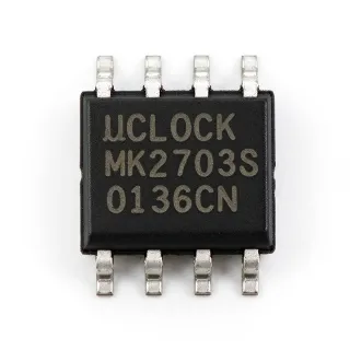
ICS409MT - 80MHz PC Peripheral Clock | Renesas Electronics
MPN: ICS409MT ✗ پایان تولیدICS409MT نمای کلی
A clock synthesizer is a timing IC that generates or distributes clock signals needed by digital logic. Clock generators and phase-locked loops sit within the clock and timing IC category, where they support processors, memory interfaces, communications equipment, and computer peripherals. By multiplying a stable reference frequency, the ICS409MT reduces the number of separate oscillators and distribution components required in a system while providing a defined LVCMOS interface for downstream circuitry.
The principal features of the ICS409MT are its 80 MHz maximum output frequency, single LVCMOS output, single PLL, crystal input, and 1:3 input-to-output ratio. The 14.31818 MHz reference arrangement supports designs based on the traditional PC timing domain, while the on-chip oscillator eliminates the need for an external oscillator module. The 8-SOIC surface-mount package also supports compact, automated PCB assembly compared with larger through-hole clock packages.
Technically, the ICS409MT is identified as a PLL-based clock and frequency synthesizer with one clock circuit. The oscillator and PLL establish the output timing relationship between the crystal reference and the LVCMOS clock output. The listed 1:3 ratio indicates that the output clock is three times the reference frequency, producing 42.95454 MHz when operated with a 14.31818 MHz crystal. Input and output polarity, PLL loop bandwidth, jitter, output duty-cycle limits, and detailed electrical timing values require confirmation from the manufacturer datasheet before final timing-budget work.
Typical applications include PC peripheral clock generation, legacy computer interface cards, embedded systems that use a 14.31818 MHz reference, communication equipment, and digital subsystems requiring a locally generated LVCMOS clock. In these systems, the device can centralize clock multiplication and reduce oscillator-component count. Its 80 MHz ceiling provides useful headroom when the intended peripheral clock is 42.95454 MHz, while the single-output architecture suits designs that need one derived clock rather than several independently managed clocks.
The primary design consideration is crystal and layout stability. Place the crystal, load capacitors, and ground path close to the device, and route high-current clock output away from sensitive analog and communication signals. Validate the resulting clock against the system’s frequency tolerance, jitter, rise-time, duty-cycle, and load requirements. Because the documented operating range is 0°C to 70°C, the part should not be assumed suitable for industrial temperature environments without additional qualification.
This product record combines the device architecture, package information, operating limits, search-oriented technical questions, application guidance, and engineering-selection context. It also clearly separates confirmed characteristics from parameters that require datasheet confirmation, helping designers evaluate ICS409MT before committing it to a PC peripheral, legacy computing, or embedded clock-generation design.
جایگزینهای drop-in برای ICS409MT — همان پکیج، سازگار پینبهپین. قطعات با پکیج متفاوت که نیاز به تغییر PCB دارند مستثنی هستند.
هیچ جایگزین مستقیمی برای این محصول موجود نیست.
درخواست جایگزینICS409MT مشخصات
| Device Type | Clock/Frequency Synthesizer |
| PLL | Yes |
| Number of Circuits | 1 |
| Input Type | Crystal |
| Reference Crystal Frequency | 14.31818 MHz |
| نوع خروجی | LVCMOS |
| Maximum Output Frequency | 80 MHz |
| Input-to-Output Ratio | 1:3 |
| محدوده دمای کاری | 0°C to 70°C |
| بستهبندی | 8-SOIC |
| Package Width | 3.90 mm |
| نوع نصب | Surface Mount (SMD/SMT) |
| Packaging Type | Reel (TR) |
راهنمای پیکربندی پین ICS409MT 3.90 mm
پیکربندی پین برای ICS409MT (پکیج 3.90 mm). شمارهگذاری پایهها، عملکردها و نمودارهای اتصال در دیتاشیت سازنده تعریف شده است. برای footprint دقیق و دستورالعملهای لحیمکاری به آن مراجعه کنید.

داده پینآوت تفصیلی موجود نیست برای ICS409MT.
به دیتاشیت برای پیکربندی کامل پینها.
کاربردهای معمول
ICS409MT مناسب است برای 6 کاربردs: Legacy PC Peripheral Clocking, Communication Interface Cards, Embedded Legacy Control Systems, Industrial Data Acquisition Equipment, Computer Expansion and Adapter Cards, Digital Peripheral Clock Distribution.
Legacy PC Peripheral Clocking
The ICS409MT fits legacy PC peripheral designs that use a 14.31818 MHz reference and require a derived LVCMOS clock. Its on-chip crystal oscillator and documented 1:3 ratio produce a nominal 42.95454 MHz output, avoiding the need for a separate oscillator in designs intended to remain close to the original PC timing architecture. The 8-SOIC package is suitable for automated assembly, and the 80 MHz maximum output frequency provides design margin above the nominal operating point. Before release, confirm supply voltage, output loading, duty-cycle limits, jitter, and the complete pin configuration from the manufacturer datasheet.
پیشنهادی
Communication Interface Cards
The ICS409MT can support communication interface cards that inherit the 14.31818 MHz timing reference used in PC peripheral designs. Its single LVCMOS output provides a local clock source for digital logic, while the documented 80 MHz ceiling accommodates a 42.95454 MHz output produced by the 1:3 ratio. Integration is most appropriate where the existing board already follows this reference architecture and only one derived clock is required. Validate clock edge quality, load capacitance, return path, and EMI behavior because the available records do not define jitter, duty cycle, or rise and fall times.
پیشنهادی
Embedded Legacy Control Systems
The ICS409MT is applicable to embedded systems that retain a 14.31818 MHz crystal and derive a higher-frequency processing or peripheral clock. The 1:3 ratio gives a nominal 42.95454 MHz LVCMOS clock, and the single PLL-based circuit allows the reference frequency to be multiplied without a separate oscillator component. Its 0°C to 70°C operating range suits room-temperature equipment but not extended industrial environments without further qualification. The design should include close crystal placement, defined load capacitance, solid grounding, and a timing budget based on verified electrical characteristics.
پیشنهادی
Industrial Data Acquisition Equipment
The ICS409MT can serve as a local clock element in data-acquisition equipment built around legacy PC timing or an existing 14.31818 MHz reference. A single 42.95454 MHz LVCMOS output may support digital conversion, buffering, or interface logic when that frequency matches the system architecture. Because the device has one output and an 80 MHz maximum, systems requiring multiple synchronized clocks need additional distribution or synthesis stages. Confirm output current, duty-cycle distortion, jitter, load behavior, and supply limits before using it in precision measurement equipment.
پیشنهادی
Computer Expansion and Adapter Cards
The ICS409MT is well aligned with expansion and adapter cards designed around traditional PC peripheral clocking. Its crystal input, on-chip oscillator, and 1:3 multiplication ratio reduce the number of timing components needed when the board expects a 42.95454 MHz clock derived from 14.31818 MHz. The surface-mount SOIC-8 package supports automated assembly and compact routing. Because the part is obsolete and specified only for 0°C to 70°C operation, it is most appropriate for maintenance, replication, or controlled legacy production rather than new long-life platforms.
پیشنهادی
Digital Peripheral Clock Distribution
The ICS409MT can provide the upstream clock for a digital peripheral subsystem that requires one LVCMOS waveform and already uses a 14.31818 MHz reference. Its stated 1:3 ratio and 80 MHz maximum make it suitable for generating a nominal 42.95454 MHz clock and then distributing that signal through the board. The single-output limit means fanout buffers may be required when several destinations need independent buffering. Layout should keep the oscillator loop compact, provide a low-impedance ground, and isolate the clock from sensitive inputs to reduce susceptibility to radiated and conducted noise.
پیشنهادی
خلاصه محصولات پیشنهادی
دادههای مرجع مهندسی برای ICS409MT — مقایسه، راهنمای طراحی و اطلاعات انطباق.
راهنمای انتخاب
مقایسه با جایگزینها
| پارامتر | این محصول |
|---|---|
| Brand | Renesas Electronics |
| Package | 8-SOIC |
| Device Type | Clock/Frequency Synthesizer |
| Maximum Output Frequency | 80 MHz |
| Input Type | Crystal |
| Reference Crystal Frequency | 14.31818 MHz |
| Output Type | LVCMOS |
| Input-to-Output Ratio | 1:3 |
| Number of Circuits | 1 |
| Operating Temperature Range | 0°C to 70°C |
| Lifecycle Status | Obsolete (EOL) |
تفاوتهای کلیدی
- Purpose-built PC peripheral clock architecture (در مقابلGeneral-purpose multi-output clock synthesizers)
- Documented 80 MHz maximum output (در مقابلLower-frequency fixed clock oscillators)
- Compact surface-mount implementation (در مقابلLarger through-hole oscillator packages)
یادداشتهای طراحی
Keep the 14.31818 MHz crystal, its load network, and the associated ICS409MT pins within a compact loop on the PCB. Use the shortest practical ground return and place the crystal where mechanical vibration and temperature gradients are minimized. Avoid routing the oscillator region beneath switching nodes or high-current return paths. The exact load capacitance and grounding topology should follow the manufacturer’s recommended application circuit because those details are not established by the available device summary.
Treat the LVCMOS clock as a timing signal whose edge rate, duty cycle, and loading can affect downstream circuitry. Confirm the output-current capability, capacitive-load limit, rise and fall times, and maximum output frequency from the manufacturer datasheet. Use a short point-to-point route from the clock output to the first receiver or distribution buffer, provide a continuous reference plane, and avoid unnecessary stubs when the clock feeds more than one destination.
Do not infer that all related ICS409 order codes are interchangeable. The ICS409MT record specifically identifies an 8-SOIC package, reel packaging, surface mounting, and a 0°C to 70°C range. Confirm the complete pin map, supply voltage, absolute maximum ratings, and crystal requirements before schematic capture. Also account for the obsolete lifecycle status in availability planning and in any long-term production commitment.
اطلاعات انطباق
No specific RoHS, REACH, lead-free, halogen-free, or conflict-minerals statement is established for this obsolete device.