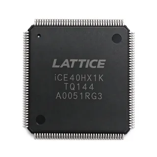
LFE2-12E-5T144C - 12K LUT FPGA, 93 I/O, 144-TQFP | Lattice Semiconductor
MPN: LFE2-12E-5T144C ✗ پایان تولیدLFE2-12E-5T144C نمای کلی
An FPGA is a programmable semiconductor whose lookup tables, registers, interconnect resources, and dedicated blocks can be configured after manufacture. The LFE2-12E-5T144C belongs to the broader hierarchy of FPGA and CPLD devices, within programmable logic and digital integrated circuits. Its 12K logic-cell configuration provides substantially more parallel logic capability than a small programmable logic device while retaining a conventional 144-pin package for board-level integration.
The key specifications identify 12K LUTs, 93 I/O, DSP capability, 1.2 V operation, 90 nm process technology, and a -5 speed designation. The 144-pin TQFP package exposes 144 terminals in a square gull-wing format. The LatticeECP2 family is intended for designs requiring more logic than a basic CPLD while retaining a conventional package and a broad selection of I/O resources.
The FPGA architecture allows multiple logic functions to be implemented in parallel, including control logic, data acquisition functions, protocol interfaces, and embedded signal-processing blocks. The dedicated DSP capability is useful when the design benefits from hardware-accelerated arithmetic rather than a processor-intensive implementation. The 1.2 V core supply is an important consideration for board-level power planning and decoupling.
Typical applications include industrial automation, communication interfaces, consumer control logic, embedded systems, and general-purpose digital logic. A design can use the FPGA for parallel interface handling, sensor data acquisition, control sequencing, or custom peripheral logic. The 93 I/O count provides connections to external sensors, transceivers, memories, displays, and other digital components.
When laying out the circuit, place input and output decoupling capacitors close to the appropriate power pins and route high-speed or sensitive signals away from noisy switching nodes. Confirm the pin assignments, supply requirements, configuration method, and unused-pin treatment in the manufacturer datasheet before fabrication. Use the Request a Quote form on this page for current availability and sourcing requirements.
جایگزینهای drop-in برای LFE2-12E-5T144C — همان پکیج، سازگار پینبهپین. قطعات با پکیج متفاوت که نیاز به تغییر PCB دارند مستثنی هستند.
گونهها در این سری
مدلهای همسری که جایگزین مستقیم هستند برای LFE2-12E-5T144C (همان فرمفاکتور و فوتپرینت) — متفاوت در Device Type, Package, Speed Grade, Process Technology.
LFE2-12E-5TN144C
✅ جایگزین مستقیم📋 جایگزین مرجع (خارج از کاتالوگ)
LFE2-12E-7T144C
✅ جایگزین مستقیمبرای قیمت تماس بگیرید
مشاهده دیتاشیت ←LFE2-12SE-5TN144C
✅ جایگزین مستقیم📋 جایگزین مرجع (خارج از کاتالوگ)
LFE2-12SE-6TN144C
✅ جایگزین مستقیم📋 جایگزین مرجع (خارج از کاتالوگ)
LFE2-12E-5Q208C
✅ جایگزین مستقیمبرای قیمت تماس بگیرید
مشاهده دیتاشیت ←LFE2-12E-5T144C حداکثر مقادیر مجاز و مشخصات الکتریکی
| Device Type | Field Programmable Gate Array (FPGA) |
| FPGA Family | LatticeECP2 |
| Logic Cells | 12,000 cells |
| Lookup Tables | 12K LUTs |
| I/O Count | 93 I/O |
| DSP Capability | DSP: 1 |
| Core Voltage | 1.2 V |
| Speed Grade | -5 speed grade |
| Process Technology | 90 nm |
| بستهبندی | 144-pin TQFP |
| Package Type | LQFP / TQFP |
| Terminal Count | 144 terminals |
| Package Shape | Square |
| Terminal Form | Gull wing |
| Temperature Grading | Other |
| Datasheet File Size | 26,538 KB |
راهنمای پیکربندی پین LFE2-12E-5T144C square
پیکربندی پین برای LFE2-12E-5T144C (پکیج square). این IC دیجیتال شامل GPIO، رابطهای ارتباطی (UART، SPI، I2C) و پینهای تغذیه است. برای عملکردهای جایگزین پین و گزینههای پیکربندی به دیتاشیت سازنده مراجعه کنید. ضروری برای طراحی سیستمهای نهفته و چیدمان PCB.

داده پینآوت تفصیلی موجود نیست برای LFE2-12E-5T144C.
به دیتاشیت برای پیکربندی کامل پینها.
کاربردهای معمول
LFE2-12E-5T144C مناسب است برای 7 کاربردs: Industrial Automation Control, Communication Interface Bridging, Data Acquisition Systems, Embedded System Peripherals, Video and Display Control, Sensor Signal Processing, Consumer and Portable Logic.
Industrial Automation Control
The LFE2-12E-5T144C fits industrial control systems that require parallel state-machine logic, timing, and interface handling without relying on a separate processor for every control function. Its 12,000 logic cells can accommodate sequencing logic, machine-state management, diagnostic counters, and signal conditioning, while 93 I/O provide connections to sensors, actuators, and industrial interfaces. The 1.2 V core operation supports modern low-voltage board design, but industrial suitability must also be evaluated against the exact temperature grade, isolation requirements, EMC design, and qualification expectations of the finished equipment.
Communication Interface Bridging
The LFE2-12E-5T144C is useful for bridging parallel and serial data paths in embedded communication equipment. The programmable logic can implement framing, byte alignment, buffering, protocol state machines, and timing constraints, while the DSP capability can support selected arithmetic functions. With 93 I/O, the device can connect data buses, control signals, and external transceivers without requiring every protocol operation to run in software. Confirm transceiver voltage levels, clock-rate requirements, and timing closure before selecting the FPGA for a specific communication standard.
Data Acquisition Systems
For data-acquisition and instrumentation designs, the LFE2-12E-5T144C can combine sensor-interface logic, parallel data capture, filtering, and control functions in one programmable device. Its 12,000 logic cells and 93 I/O allow multiple acquisition channels and supporting control paths to be implemented in parallel. The dedicated DSP capability may reduce the burden on an external processor for suitable fixed-point operations. The actual signal-chain accuracy depends on the selected I/O, ADC or sensor interfaces, clocking architecture, and analog front end, which must be designed separately.
Embedded System Peripherals
The LFE2-12E-5T144C can serve as a dedicated peripheral engine alongside a microcontroller or application processor. Offloading waveform generation, display formatting, memory-interface control, timing, and data-packing tasks can make the host processor architecture more predictable. The 12K LUT resource level is substantial enough for parallel logic and moderate protocol handling, and the 144-pin TQFP package supports conventional board assembly. System partitioning should account for bus ownership, interrupt latency, clock-domain boundaries, configuration method, and the additional board area required by the FPGA.
Video and Display Control
The LFE2-12E-5T144C is applicable to display-control and video-timing designs where programmable timing generation, pixel formatting, and control logic are required. Its parallel logic resources can process timing counters, synchronization signals, and data-path transformations, while 93 I/O provides connections to display and memory interfaces. The device should be selected only when the required pixel rate, memory bandwidth, and I/O voltage levels fit the ECP2 implementation. Use the manufacturer timing and I/O standards to confirm suitability for the target resolution and refresh rate.
Sensor Signal Processing
The LFE2-12E-5T144C can combine sensor conditioning, digital filtering, event detection, and control output in a compact programmable-logic implementation. Its DSP capability supports suitable fixed-point arithmetic, while 12,000 logic cells provide room for parallel channels and control state machines. The 93 I/O count is useful for connecting sensors, thresholds, switches, and downstream controllers. Sensor accuracy remains dominated by the analog front end and calibration process, so the FPGA should be treated as the digital processing layer rather than a substitute for appropriate sensing hardware.
Consumer and Portable Logic
The LFE2-12E-5T144C can implement programmable control, user-interface logic, peripheral emulation, and compact data-processing functions in consumer or portable equipment. Its 1.2 V core operation is compatible with modern low-voltage system design, and the 144-pin TQFP package offers a conventional assembly option. Designers should check standby-power behavior, active current, configuration retention, and startup time against the product's battery and user-experience requirements. The logic resource count also allows product differentiation through programmable behavior without changing the PCB for minor feature revisions.
دادههای مرجع مهندسی برای LFE2-12E-5T144C — مقایسه، راهنمای طراحی و اطلاعات انطباق.
راهنمای انتخاب
مقایسه با جایگزینها
| پارامتر | این محصول | LFE2-12E-5TN144C | LFE2-12E-7T144C | LFE2-12SE-5TN144C | LFE2-12SE-6TN144C | LFE2-12E-5Q208C |
|---|---|---|---|---|---|---|
| Package | 144-pin TQFP | 144-LQFP / TQFP-144 | 144-pin TQFP | PQFP144 / TQFP-144 | 144-pin TQFP | 208-pin package |
| Brand | Lattice Semiconductor | Lattice Semiconductor | Lattice Semiconductor | Lattice Semiconductor | Lattice Semiconductor | Lattice Semiconductor |
| FPGA Family | LatticeECP2 | LatticeECP2 | LatticeECP2 | LatticeECP2 | LatticeECP2 | LatticeECP2 |
| Logic Cells | 12,000 cells | 12,000 cells | 12,000 cells | 12,000 cells | 12,000 cells | 12,000 cells |
| Lookup Tables | 12K LUTs | 12K LUTs | 12K LUTs | 12K LUTs | 12K LUTs | 12K LUTs |
| I/O Count | 93 I/O | 93 I/O | 93 I/O | 93 I/O | 93 I/O | 93 I/O |
| Core Voltage | 1.2 V | 1.2 V | 1.2 V | 1.2 V | 1.2 V | 1.2 V |
| Speed Grade | -5 | -5 | -7 | -5 | -6 | -5 |
| Process Technology | 90 nm | 90 nm | 90 nm | 90 nm | 90 nm | 90 nm |
| DSP Capability | 1 DSP | 1 DSP | 1 DSP | 1 DSP | 1 DSP | 1 DSP |
تفاوتهای کلیدی
- Defined 12K-LUT resource class (در مقابلLFE2-12E-5TN144C)
- Same-family timing upgrade option (در مقابلLFE2-12E-7T144C)
- Industry-standard 144-pin square package (در مقابلLFE2-12E-5Q208C)
یادداشتهای طراحی
Use the 1.2 V core specification as the basis for supply planning, but obtain the complete power-up sequence, allowable tolerance, and I/O supply requirements from the manufacturer datasheet before fixing the regulator design. Place the required bypass capacitors at the associated power pins with short, low-inductance traces. Keep the 1.2 V core rail and I/O rails physically separated where the recommended layout calls for it, and verify the design with the Lattice power-estimation tool after the final logic and clock assignments are complete.
Build the PCB footprint from the exact 144-pin TQFP drawing for the selected ordering code, including body size, lead span, pitch, and solderable land geometry. The product is also described as LQFP or PQFP144, so a generic 144-pin footprint should not be assumed. Assign every pin from the manufacturer pin table, including configuration, supply, ground, and no-connect pins, and perform a manufacturing check for exposed thermal or thermal-pad requirements if the selected package drawing includes one.
Do not treat two ECP2 ordering codes as interchangeable solely because both are labeled 144-pin devices. The speed grade, device variant, temperature rating, and suffix can change timing, power, or ordering eligibility. Before a substitution, compare the exact manufacturer part tables, regenerate the bitstream with the replacement device selected, rerun static timing, and inspect all new configuration and I/O constraints. This prevents a mechanically similar part from causing a timing or board-level mismatch.
Route clock and high-speed interface nets with continuous reference planes and avoid stubs, test-point discontinuities, and unnecessary layer changes. Use the device's I/O timing constraints to define external delays rather than relying on nominal trace-length matching alone. For mixed-signal or sensor-facing boards, keep clocks and high-speed data away from sensitive analog inputs, provide a continuous ground reference, and follow the manufacturer guidance for unused and weakly driven pins.
اطلاعات انطباق
A comparison listing identifies the LFE2-12SE-5TN144C as lead free, but the target LFE2-12E-5T144C's own compliance status is not explicitly confirmed. RoHS, REACH, AEC-Q100, halogen-free, and conflict-minerals status remain unknown.