Semi-conducteurs discrets
Sous-catégories
Produits (1814)

IRF7495TRPBF - 100V 7.3A N-Channel MOSFET | Infineon
The Infineon IRF7495TRPBF is an N-channel power MOSFET rated at 100 V VDS and 7.3 A continuous drain current (Ta), housed in an 8-pin SO-8 surface-mount package. Built on Infineon's IR MOSFET technology platform, it delivers a low typical on-resistance of 22 mOhm and a low gate-to-drain charge designed to reduce switching losses in high-frequency converter stages. A power MOSFET is a voltage-controlled semiconductor switch used in power conversion circuits. The N-channel enhancement-mode MOSFET sits within the broader hierarchy of power discrete semiconductors: MOSFET -> transistor -> discrete semiconductor -> semiconductor. Within power-electronics subsystems, N-channel MOSFETs such as the IRF7495TRPBF typically serve as low-side or high-side switches in DC-DC converters, motor drivers, and load-switching paths, replacing older bipolar transistors because they require essentially no steady-state gate drive current. Key parametric strengths include a maximum drain-source voltage of 100 V, continuous drain current of 7.3 A at TA=25 C, and pulsed drain current capability suitable for transient loads. The device features an ultra-low gate charge of 34 nC typical and maximum RDS(on) of 22 mOhm at VGS=10 V, ID=4.4 A. These parameters translate to lower conduction losses and reduced gate-drive requirements, which simplifies the upstream PWM controller selection. Architecturally, the IRF7495TRPBF uses a planar-style trenchFET-class cell design with a low figure-of-merit (RDS(on) x Qg) optimized for synchronous rectification. The fully characterized capacitance profile, including effective COSS, simplifies the calculation of dead-time and resonant-tank behavior in LLC, half-bridge, and active-clamp forward topologies. The standard SO-8 footprint allows direct drop-in replacement into existing layouts without PCB rework. Typical applications include high-frequency DC-DC converters (synchronous-rectifier and primary-side switch), high-side load switches in telecom and networking equipment, battery protection circuits in 12 V to 36 V packs, and motor-drive H-bridges up to a few hundred watts. The 100 V rating provides adequate margin for 24 V industrial buses and 48 V telecom rails. When designing with this part, ensure VGS is driven to at least 10 V for full enhancement into the lowest RDS(on) region. A low-impedance gate-drive path with a series gate resistor of 10 to 100 ohm is recommended to control ringing and EMI. The SO-8 thermal pad should be soldered to a copper pour of at least 1 square inch to keep junction temperature within safe limits at full load. This page synthesizes distributor pricing, drop-in alternatives in the same SO-8 footprint, and practical design notes not found in the manufacturer datasheet alone.

IRF7749L1TRPBF - 60V N-Channel HEXFET MOSFET DirectFET L8
The Infineon IRF7749L1TRPBF is a 60 V, N-Channel HEXFET power MOSFET in a surface-mount DirectFET Isometric L8 package rated for 33 A continuous drain current at TA=25 C and 200 A pulsed at TC=25 C, with a maximum on-resistance of 1.5 mOhm at VGS=10 V. A power MOSFET is a voltage-controlled metal-oxide-semiconductor field-effect transistor designed to switch or amplify power in electronic systems. The IRF7749L1 belongs to the HEXFET Power MOSFET family, a N-Channel enhancement-mode device in the DirectFET (L8 isometric) surface-mount package. The DirectFET package provides a top-side cooling path through a metal can, dramatically lowering thermal resistance compared to standard SO-8 or DPAK packages, which is critical for high-current DC-DC conversion where every milliohm of RDS(on) counts. Key features include an ultra-low typical on-resistance of 1.1 mOhm at VGS=10 V, a 2.9 V minimum gate-threshold rating optimized for logic-level and standard 5 V gate drive, and a continuous drain current of 200 A at TC. The device also offers a low total gate charge of 200 nC maximum, a maximum drain-source voltage of 60 V, and a junction-to-ambient thermal resistance of 45 K/W. The DirectFET L8 package allows top-side cooling via the metal can. The IRF7749L1 is built on Infineon's IR MOSFET silicon technology with an optimized cell structure that minimizes RDS(on) per unit area while maintaining avalanche ruggedness. The DirectFET L8 isometric package eliminates wire bonds and exposes the silicon die directly to a top-side metal can for double-sided cooling, which improves both thermal performance and current-handling density. The 2.9 V gate threshold ensures clean enhancement with low-voltage gate drivers and microcontrollers. Typical applications include synchronous rectification in high-current DC-DC converters, high-density VRM and POL modules for servers and datacenters, OR-ing FETs in redundant power systems, hot-swap controllers on 48 V telecom boards, and high-current motor drive bridges. The combination of 1.1 mOhm RDS(on) and DirectFET thermal performance makes it ideal for point-of-load converters requiring high efficiency at >30 A per phase. When designing with this part, observe the SOA carefully because pulsed drain current of 200 A is only achievable with substantial case cooling; at TA=25 C with minimum footprint copper, expect continuous current closer to 33 A. The DirectFET L8 footprint requires precise land pattern adherence per Infineon's application note, and a top-side thermal pad or heatsink should be considered for high-duty-cycle operation. This page synthesizes distributor pricing, drop-in alternatives, and DirectFET-specific design notes not found in the manufacturer datasheet alone, helping engineers evaluate the IRF7749L1TRPBF for high-current DC-DC applications.
IRF7769L1TRPBF - 100V N-Channel HEXFET MOSFET | Infineon
The Infineon IRF7769L1TRPBF is a 100 V single N-channel HEXFET power MOSFET housed in a DirectFET Isometric L8 surface-mount package with only 0.7 mm profile. It is rated for 20 A continuous drain current at TA=25C, 124 A at TC=25C, with 3.3 W power dissipation at TA and 125 W at TC. The die uses Infineon's latest-generation HEXFET silicon technology to deliver a maximum on-state resistance of 3.5 mOhm at VGS=10 V and a low typical gate charge of 200 nC, making it well suited to high-frequency switching and synchronous rectification. A power MOSFET is a voltage-controlled semiconductor switch that conducts current between drain and source when VGS exceeds the gate threshold; the N-channel enhancement-mode variant is the workhorse of switched-mode power supplies, motor drives, and OR-ing functions. Within the broader taxonomy it sits under discrete semiconductors -> transistors -> MOSFETs -> power MOSFETs -> N-channel enhancement-mode. DirectFET packaging removes the plastic molding and lead frame found in D2PAK or SO-8 parts, exposing the silicon die to the PCB for direct top-side cooling and dramatically reducing source-inductance parasitic losses. Key features include 3.5 mOhm maximum RDS(on) at 10 V VGS, a logic-level-friendly 4.5 V gate drive capability, a 100 V VDS rating that gives substantial headroom for 48 V telecom and industrial bus rails, and a thermally efficient DirectFET L8 land pattern. The package footprint is smaller than a D2PAK while achieving lower junction-to-case thermal resistance, enabling higher power density on the same board area. The IRF7769L1 is optimized for high-frequency switching and synchronous rectification applications. The reduced total gate charge and switching losses, combined with the high thermal performance of DirectFET, allow high efficiency at elevated switching frequencies - critical for system reliability and for shrinking magnetics in isolated DC-DC converters. The device is qualified to MSL1 and supports lead-free, halogen-free reflow up to 260C. Typical applications include isolated DC-DC converter primary-side switches, synchronous rectification on secondary-side low-voltage rails, hot-swap and OR-ing controllers in 48 V telecom systems, and high-current POL (point-of-load) converters. The 124 A pulsed rating also makes the part attractive for motor-drive half-bridges and e-fuse circuits. When designing with this device, follow DirectFET land-pattern guidelines and use the top-side thermal pad or copper pour to conduct heat away from the die. Gate-drive resistors of 5-10 ohm are recommended to suppress ringing at switching frequencies above 500 kHz, and the source-sensing pin should be tied directly to the source pad to avoid Cdv/dt-induced turn-on. This page synthesizes distributor pricing, drop-in alternatives, and practical design notes not found in the manufacturer datasheet, enabling engineers to evaluate fit, sourcing, and PCB layout decisions in one place.
IRF7779L2TRPBF - 150V 67A HEXFET N-Channel MOSFET | Infineon
The Infineon IRF7779L2TRPBF is a 150 V N-channel HEXFET power MOSFET rated for 67 A continuous drain current (Tc) in a surface-mount DirectFET Isometric L8 package. According to the manufacturer datasheet, it combines IR HEXFET silicon technology with the DirectFET platform to deliver an RDS(on) of 7.7 mOhm (typical) / 11 mOhm (max) at VGS = 10 V, with a low 0.7 mm profile that fits footprints smaller than D2PAK. A power MOSFET (Metal-Oxide-Semiconductor Field-Effect Transistor) is a voltage-controlled three-terminal switch used for power conversion and switching. Within the device taxonomy, the IRF7779L2 sits in the N-channel enhancement-mode MOSFET family, which is the dominant topology for low-side and synchronous-rectifier switching in modern SMPS designs because N-channel carriers offer ~2-3x lower RDS(on) per unit silicon area than equivalent P-channel parts. Key features include a 150 V drain-to-source breakdown voltage, 67 A continuous drain current (Tc) and 11 nC total gate charge. Power dissipation is rated 3.3 W at TA=25C and 125 W at Tc=25C, supporting both thermally-limited PCB designs and large-conduction heatsink-based layouts. The DirectFET L8 case is dual-side cooled via metal can construction, removing the need for an external thermal pad and reducing package parasitic inductance versus D2PAK/TO-220. The device uses Infineon's fifth-generation HEXFET trench process, achieving low figure-of-merit (FOM = RDS(on) x Qg) for high-frequency isolated-converter primary-side switching. Optimized for hard-switched topologies up to several hundred kHz, it is also suited for OR-ing and hot-swap roles where low conduction loss matters more than switching speed. Typical applications include isolated DC-DC converter primary switches in telecom bricks, server and datacom 48 V intermediate bus converters, motor-drive H-bridges (low-side position), hot-swap / eFuse circuits, and battery protection FETs in 96-100 V lithium packs. The 150 V rating gives comfortable margin below the 100 V telecom bus. When designing with this part, follow DirectFET land-pattern guidelines exactly - the metal can doubles as the drain terminal and requires precise stencil apertures for the side-cooling vias. VGS(th) is in the 2-4 V range, so a 10 V gate drive is mandatory for full RDS(on) and lowest conduction loss. This page consolidates distributor pricing, same-footprint DirectFET alternatives, and DirectFET-specific design notes not found on stock catalog pages.

IRF7815TRPBF - 150V N-Ch HEXFET MOSFET 5.1A | Infineon
The Infineon IRF7815TRPBF is a 150V N-channel HEXFET power MOSFET rated at 5.1A continuous drain current (at TA=25C) and 43 mOhm maximum on-resistance, housed in an 8-pin SO-8 surface-mount package. It is built on Infineon's IR MOSFET process, optimized for high-efficiency synchronous rectification in isolated DC-DC converters and synchronous buck stages for notebook processor power. A power MOSFET is a voltage-controlled semiconductor switch that uses an insulated gate to modulate current flow between its drain and source terminals. HEXFET is Infineon's trade name for its planar power-MOSFET cell architecture; within the broader taxonomy, HEXFET MOSFETs belong to the discrete power MOSFET family, which sits under transistors, FETs, and the wider discrete semiconductor category used in power management. Compared with bipolar transistors, MOSFETs switch faster, require essentially no DC gate current, and integrate easily into high-frequency switch-mode power supply (SMPS) topologies. Key specifications include a 150V drain-to-source breakdown voltage, 43 mOhm maximum Rds(on) at Vgs=10V, 25 nC typical total gate charge, and 2.5W maximum power dissipation on the SO-8 PCB footprint. The part also features low gate charge for reduced driver losses, an avalanche-rated body diode, and a logic-compatible gate threshold suitable for 10V standard gate-drive rails. Its 8-pin SO-8 package allows compact layout for point-of-load converters where PCB area is constrained. Architecturally, the IRF7815 uses a strip-cell planar DMOS design that balances low on-resistance with robust avalanche energy. The IR MOSFET process delivers a tight Rds(on) distribution and strong dynamic performance at 100 kHz to 1 MHz switching frequencies commonly seen in modern VRM and telecom DC-DC bricks. Compared with trench-generation devices, this planar technology typically provides a more rugged body diode, which simplifies synchronous-rectifier dead-time control. Typical applications include synchronous rectification in isolated telecom DC-DC converters, high-side and low-side switches in notebook CPU buck regulators, POL converters for networking ASICs, and 48V bus point-of-load conversion in industrial equipment. The 150V rating also makes it suitable for 24V/36V industrial and telecom intermediate bus architectures. When designing with this MOSFET, ensure the SO-8 copper pad area delivers a junction-to-ambient thermal resistance that keeps the die within safe temperature limits at full load. Use a gate-driver capable of pulling the gate to at least 10V to achieve the rated Rds(on), and include a small gate-source resistor to suppress ringing. This page synthesizes distributor pricing, drop-in same-package alternatives, and practical design notes not found in the manufacturer datasheet alone.

IRF7832TRPBF - 30V N-Channel HEXFET MOSFET, 20A, SO-8 | Infineon
The Infineon IRF7832TRPBF is a 30V N-Channel HEXFET power MOSFET housed in an 8-SO (SOIC-8) surface-mount package, rated for 20A continuous drain current at TA and 4 mOhm maximum on-resistance at VGS=10V. Originally released by International Rectifier and now manufactured by Infineon, this part targets high-efficiency synchronous rectification in DC-DC converter stages where minimal conduction loss and small PCB footprint are required. A power MOSFET such as the IRF7832TRPBF is the active switching element in a synchronous buck or synchronous boost converter. The MOSFET controls current flow between the input supply and the inductor/transformer during the high-side and low-side switching intervals. Compared to a Schottky rectifier, a low-RDS(on) synchronous MOSFET dramatically reduces conduction loss, raising overall converter efficiency by 3-7 percent at full load. The IRF7832TRPBF belongs to the discrete power MOSFET family within Infineon's HEXFET product line, characterized by a vertical DMOS cell structure and a trench-gate process that minimize both on-resistance and gate charge. Key specifications include a VDS rating of 30V, VGS of +/-20V maximum, a continuous ID of 20A at TA=25C, an RDS(on) maximum of 4 mOhm at VGS=10V, and a total gate charge of 34 nC typical. The threshold voltage (VGS(th)) is typically in the 1.0V to 2.5V range. The SO-8 package provides low thermal resistance when mounted on a 1-square-inch copper pad, enabling 2.5W dissipation at TA=25C without an external heatsink. The HEXFET process uses a vertical DMOS architecture with planar cell geometry, yielding extremely low on-resistance per unit silicon area. This allows Infineon to fit a 20A/30V die into the small SO-8 outline, delivering DPAK-class performance at roughly one-third the board area. The 34 nC total gate charge keeps switching losses low at frequencies up to 500 kHz in synchronous rectifier positions. Typical applications include synchronous rectification in notebook processor VRM stages, isolated DC-DC converter secondary-side rectifiers in networking switches, point-of-load (POL) modules, and battery protection circuits in 1- to 4-cell lithium-ion packs. The 30V rating provides ample margin for 12V bus systems handling transients up to 20V. When designing with the IRF7832TRPBF, ensure the gate drive voltage swings above 10V to achieve the rated 4 mOhm on-resistance, and place the gate series resistor (typically 4.7-10 ohm) close to the device to suppress ringing. The SO-8 thermal pad must be soldered to a copper pour of at least 1 square inch to meet the 2.5W power dissipation rating. This page synthesizes distributor pricing, SO-8 drop-in alternatives, and practical synchronous-rectifier design guidance not aggregated on a single manufacturer or distributor product page.
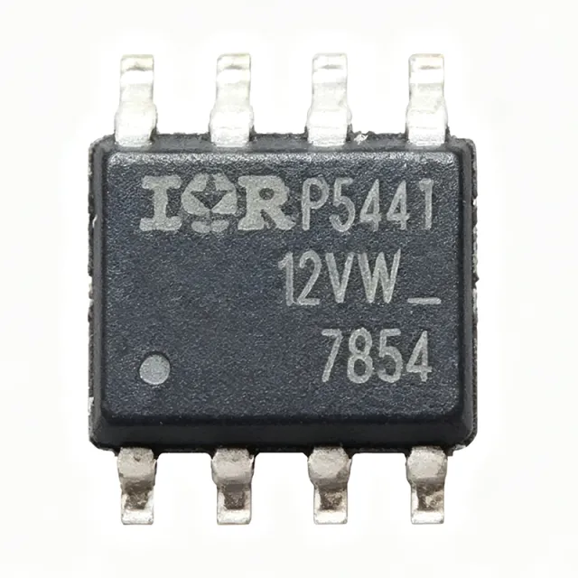
IRF7854TRPBF - 80V 10A N-Channel HEXFET MOSFET SO-8 | Infineon
The Infineon IRF7854TRPBF is an 80 V single N-channel HEXFET power MOSFET housed in a lead-free SO-8 surface-mount package, rated for 10 A continuous drain current (Ta) and 2.5 W power dissipation. Per the Infineon IRF7854 datasheet, the device is optimized for 10 V gate drive, has a maximum on-resistance of 13.4 mΩ at VGS = 10 V, and is qualified to JEDEC standards for the industrial market. The 'TRPBF' suffix denotes tape-and-reel packaging with lead-free (Pb-free) terminal finish. An N-channel power MOSFET is a voltage-controlled three-terminal transistor used to switch or amplify DC loads. In the semiconductor taxonomy it sits under discrete semiconductors > transistors > MOSFETs > power MOSFETs. HEXFET is Infineon's (formerly International Rectifier) trademarked planar MOSFET technology using a hex-cell gate structure to minimize RDS(on) per unit silicon area. The N-channel variant requires a positive gate-source voltage to turn on and is the dominant polarity for low-voltage switching because electron mobility in silicon is roughly 2-3x higher than hole mobility, yielding lower on-resistance for the same die size. Key features of the IRF7854TRPBF include VDS = 80 V, ID = 10 A at 25 °C case temperature, RDS(on) = 13.4 mΩ maximum at VGS = 10 V, VGS(th) = 4.9 V maximum, total gate charge (Qg) of 27 nC, and an industry-standard SO-8 footprint. The SO-8 package exposes the die to the PCB through a large drain tab (pin 5-8), enabling reasonable thermal performance without an external heatsink at moderate duty cycles. The device is also wave-solderable, simplifying mixed-technology assembly. Architecturally, the IRF7854 uses Infineon's mature HEXFET planar stripe-cell process, which trades off slightly higher RDS(on) for exceptional ruggedness, high avalanche energy, and very low gate charge for the voltage class. The result is a robust 80 V part suitable for primary-side switching in telecom bricks, DC-DC converters, and motor drive H-bridges where inductive avalanche events are routine. Typical applications include primary-side switches in 48 V telecom rectifier modules (within the 48 V ETSI input range), synchronous rectification in isolated DC-DC converters, half-bridge motor drivers, battery protection circuits in 24-36 V packs, and hot-swap controllers for 48 V backplane distribution. The part is also widely used in Class-D audio output stages and e-bike controller boards. When designing with this part, ensure that VGS is driven to at least 10 V for full RDS(on) performance; logic-level 3.3 V MCUs will not turn the device fully on and will incur excessive conduction loss. For high-side use, a gate-drive bootstrap or isolated supply is required because the source pin swings with the load. This page synthesizes distributor stock data, cross-reference equivalents, and practical design notes that are not consolidated in the manufacturer datasheet, giving engineers a single source for sourcing and second-source decisions.

IRF7907TRPBF - Dual N-Ch 30V 9.1A/11A MOSFET | Infineon SO-8
The Infineon IRF7907TRPBF is a dual N-channel power MOSFET array built on Infineon's IR MOSFET technology, rated at 30 V VDS, 9.1 A continuous ID per channel (11 A pulsed), and housed in an industry-standard 8-pin SO-8 (SOIC-8) surface-mount package. The part is supplied on tape and reel (TR) and is lead-free (PBF suffix), making it suitable for automated high-volume assembly. A power MOSFET is a voltage-controlled semiconductor switch that uses an electric field at the gate to control current flow between drain and source. As a dual N-channel device, the IRF7907TRPBF integrates two independent MOSFETs on a single die, allowing engineers to replace two discrete transistors with one part - saving PCB area, simplifying layout, and reducing parasitic inductance in synchronous buck or half-bridge topologies. Key specifications from the manufacturer product page include a maximum drain-source voltage of 30 V, a maximum on-resistance of 11.8 mOhm at VGS = 10 V (with some sources citing 9.8 mOhm typical), a continuous drain current of 9.1 A per channel at 25 C, and a pulsed current capability of 11 A. The SO-8 package is rated for 2 W total power dissipation. Gate threshold voltage (VGS(th)) is approximately 1.35 V, supporting logic-level drive from 3.3 V or 5 V microcontrollers. The IRF7907 family leverages Infineon's IR MOSFET technology, which uses a hexfet-style trench structure to minimize R DS(on) per unit silicon area. The low on-resistance reduces conduction losses in continuous-current applications, while the low gate charge enables fast switching transitions that reduce switching losses at higher frequencies. Typical applications include point-of-load (POL) synchronous buck converters, DC motor drivers, battery protection circuits, load switches, and power-ORing circuits in computing and telecom equipment. The dual-channel configuration makes the part especially attractive for synchronous rectification where one FET acts as the control switch and the other as the freewheeling switch. When designing with this part, ensure the gate-drive voltage is at least 10 V to achieve the rated R DS(on). At high load currents, calculate conduction losses as P = I^2 x R DS(on) and verify the SO-8 thermal pad footprint is adequately copper-clad to keep junction temperature within the 150 C maximum. This page synthesizes distributor pricing, drop-in alternatives, and practical design notes not found on the manufacturer datasheet alone.
IRF8714TRPBF - 30V 14A 8.7mΩ N-Ch HEXFET MOSFET | Infineon
The Infineon IRF8714TRPBF is a 30 V single N-channel StrongIRFET power MOSFET rated for 14 A continuous drain current and an on-state resistance of 8.7 mΩ, housed in a surface-mount 8-pin SO-8 package. It combines Infineon's HEXFET technology with the SO-8 footprint to deliver a high-current, low-RDS(on) device suitable for both DC-DC conversion and load switching. Typical gate charge is 8.1 nC, enabling fast switching transitions at moderate gate-drive currents. An N-channel MOSFET (Metal-Oxide-Semiconductor Field-Effect Transistor) is a voltage-controlled three-terminal device in which a positive gate-to-source voltage creates a conductive channel between drain and source. N-channel MOSFETs are widely used as low-side or high-side switches in switching power supplies, motor drivers, and load management circuits because of their low on-state resistance and high switching speed. The IRF8714 belongs to the StrongIRFET family, which is optimized for high-current, low-voltage applications where both conduction and switching losses matter. Key features include a 30 V drain-source breakdown voltage, 8.7 mΩ maximum RDS(on) at VGS = 10 V, 14 A continuous drain current at TA = 25 °C (with 2.5 W power dissipation), and a logic-compatible 20 V maximum gate-source voltage. The SO-8 footprint offers excellent thermal conduction through the source pin and copper pad, allowing the device to drive 14 A in a compact PCB area. Avalanche-rated construction adds robustness against inductive load transients common in motor and solenoid circuits. The IRF8714 uses Infineon's proprietary planar HEXFET cell structure, which minimizes cell pitch and reduces RDS(on) × area figure of merit. Its 8.1 nC total gate charge keeps drive losses modest, and the SO-8 package provides a low thermal resistance path when soldered to a properly sized copper pour. The device is also RoHS-compliant and lead-free, meeting modern environmental requirements for consumer and industrial equipment. Typical applications include synchronous buck converters in point-of-load regulators, DC motor drive and reverse-polarity protection circuits, battery management and load switching in notebook and tablet designs, hot-swap controllers for enterprise servers, and high-current LED drivers. The 30 V rating provides ample margin for 12 V bus rails with significant transient headroom. When designing with the IRF8714TRPBF, ensure that the SO-8 thermal pad is soldered to at least 1 square inch of copper to keep junction temperature within safe limits at high currents. Use a gate resistor of 10 Ω to 100 Ω to control switching transients and avoid shoot-through in synchronous topologies. This page synthesizes distributor pricing, drop-in alternative parts, and practical PCB design notes not found in the manufacturer datasheet alone.
IRF8734TRPBF - 30V 21A N-Ch HEXFET MOSFET | Infineon | SO-8
The Infineon IRF8734TRPBF is a 30V N-channel HEXFET power MOSFET rated for 21A continuous drain current (at Ta) with a maximum on-resistance of 3.5 mOhm, housed in an 8-pin SOIC (SO-8) surface-mount package. Built on Infineon's StrongIRFET™ technology platform, it delivers 2.5W power dissipation (Ta) and 20nC total gate charge, making it a strong fit for synchronous rectification in low-voltage DC-DC converters. A power MOSFET is a voltage-controlled semiconductor switch that uses an electric field at the gate to modulate current flow between the drain and source terminals. N-channel MOSFETs such as the IRF8734TRPBF are the dominant switch type in low-voltage, high-current power conversion because their majority-carrier (electron) conduction channel yields lower on-resistance per unit silicon area than equivalent P-channel parts. The IRF8734TRPBF sits in the discrete-semiconductor hierarchy as a MOSFET, which itself belongs to the broader family of field-effect transistors (FETs) under power management semiconductors. Key specifications of the IRF8734TRPBF include a 30V drain-source breakdown voltage, 21A continuous drain current at 25C ambient, an industry-leading 3.5 mOhm maximum RDS(on) at VGS = 10V, and a fully characterized avalanche voltage rating. The SO-8 footprint integrates the synchronous MOSFET into compact synchronous buck converters where PCB real estate is at a premium. The device's very low RDS(on) at 4.5V VGS also allows direct logic-level drive from 5V PWM controllers without a charge-pump bootstrap stage. Architecturally, the IRF8734TRPBF uses Infineon's HEXFET cell structure with a strip-layout planar gate that minimizes cell pitch and shrinks the die, contributing to both low RDS(on) and low gate charge. The combination of 20nC Qg and 3.5 mOhm RDS(on) yields an excellent figure of merit (FOM = RDS(on) x Qg) for high-frequency switching converters operating above 500 kHz. Typical applications include synchronous rectification in isolated DC-DC converters for networking/telecom systems, low-side switch in notebook adapter power stages, CPU VCORE synchronous buck converters, and OR-ing FETs in redundant power architectures. The 30V rating provides comfortable margin for 12V rails with inductive ringing transients. When designing with the IRF8734TRPBF, prioritize gate-drive loop minimization: keep the gate-driver-to-gate trace under 5mm and use a 10 Ohm gate resistor to dampen ringing. The SO-8 package thermal pad must be soldered to a copper pour of at least 1 square inch to stay within SOA at sustained 21A loads. This page synthesizes distributor pricing, drop-in alternatives, and practical design notes not found in the manufacturer datasheet.
IRF8736PBF - 30V 18A N-Channel HEXFET MOSFET SO-8 | Infineon
The Infineon IRF8736PBF is a 30 V single N-channel HEXFET power MOSFET housed in an industry-standard 8-pin SO-8 surface-mount package, optimized for 5 V gate-drive operation (logic-level VGS(th)) and qualified to JEDEC standards. It delivers a continuous drain current of 18 A at TA=25 °C with a maximum on-resistance of 4.8 mΩ at VGS=10 V, and 6.0 mΩ at VGS=4.5 V, making it well suited to high-current, low-voltage switching stages. The total gate charge is 17 nC typical, and the part is fully characterized for avalanche voltage and current with 100 % tested Rg. A power MOSFET is a voltage-controlled semiconductor switch that uses an electric field at the gate to modulate conduction between drain and source. Within the broader taxonomy, the IRF8736PBF belongs to the N-channel enhancement-mode MOSFET family, which itself is a sub-class of discrete power transistors and ultimately falls under power semiconductor devices used in power management and switching conversion. MOSFETs of this type are the workhorse of synchronous rectification, where their very low RDS(on) minimizes conduction loss and improves system efficiency compared to diode-based rectification. Key features include a logic-level gate threshold that allows direct drive from 5 V microcontrollers or PWM controllers, low gate charge of 17 nC for fast switching transitions, very low RDS(on) of 4.8 mΩ at VGS=10 V to minimize I²R losses, fully characterized avalanche ruggedness, and 100 % tested gate resistance (Rg) for predictable parallel operation. The industry-standard SO-8 footprint also enables wave-soldering and standard PCB assembly flows. Internally the IRF8736PBF uses Infineon's HEXFET stripe-cell planar technology with a trench-style current-spreading layout. This cell architecture trades a slightly higher specific on-resistance than pure trench MOSFETs for an exceptionally low gate charge and proven avalanche capability, which is important in synchronous-rectifier and hot-swap applications where the body diode is repeatedly commutated. Typical applications include synchronous rectification in isolated DC-DC converters for networking and telecom systems, low-side switches in notebook processor VRM stages, battery protection and hot-swap circuits, and OR-ing FETs in redundant 12 V power architectures. The wide 30 V drain rating also gives enough margin for 19 V notebook adapters and 24 V industrial rails. When designing with this part, pay attention to PCB layout for the SO-8 drain tab. The exposed pad is the drain; without adequate copper pour the device will derate heavily at high currents. A 1 oz copper area of at least 1 in² is recommended for full 18 A operation.
IRF8736TRPBF - 30V 18A N-Channel StrongIRFET MOSFET | Infineon
The Infineon IRF8736TRPBF is a 30V single N-channel HEXFET power MOSFET in an 8-pin SO-8 package, rated for 18A continuous drain current (Ta) with 2.5W power dissipation (Ta) and a maximum on-resistance of 4.8 mOhm at VGS = 10V. It is part of Infineon's StrongIRFET family and is specifically designed as a synchronous MOSFET for notebook processor power and synchronous rectification in isolated DC-DC converters for networking systems. What is a StrongIRFET power MOSFET? StrongIRFET is Infineon's product family of low-voltage N-channel MOSFETs optimized for synchronous rectification and high-current switching applications. Within the power MOSFET taxonomy, this part sits in the sub-30V synchronous-rectifier / low-side-switch category, designed for systems where very low RDS(on), low gate charge, and a small SO-8 footprint are the primary trade-off variables. Key specifications include a maximum drain-source voltage of 30V, continuous drain current of 18A at TA = 25C, pulsed drain current capability significantly higher than the continuous rating, and a typical gate charge of 17 nC (per Mouser listing). The device is fully characterized for avalanche voltage and offers very low RDS(on) at 4.5V VGS, making it compatible with 5V gate-drive logic found in notebook VRMs and synchronous buck converters. Architecturally, the IRF8736 uses Infineon's proven HEXFET silicon technology in a standard industry SO-8 (MS-012AA) outline with a large exposed drain pad for PCB thermal dissipation. The low Qg reduces switching losses at high switching frequencies, which is critical for multi-phase VRMs where each phase operates at hundreds of kHz. Typical applications include synchronous rectification in isolated DC-DC converters for telecom/networking, low-side switches in notebook CPU/GPU buck converters, OR-ing FETs in redundant power architectures, motor drive H-bridges in low-voltage battery-powered systems, and hot-swap controllers in 12V/24V distribution. When designing with this part, ensure adequate copper pour on the SO-8 drain pad for thermal performance - the 2.5W (Ta) rating assumes a 1 sq. inch minimum copper footprint. Gate-drive voltage must remain above 4.5V for full enhancement, and a small gate-source resistor (10-100 ohm) is recommended to suppress ringing. This page synthesizes distributor pricing, drop-in same-package alternatives, and practical PCB layout notes not found in the manufacturer datasheet.
IRF9383MTRPBF - 30V P-Channel HEXFET MOSFET, 160A | Infineon
The Infineon IRF9383MTRPBF is a -30V single P-Channel HEXFET Power MOSFET in a surface-mount DIRECTFET MX package, rated for 22A continuous drain current at Ta (or 160A at Tc) with power dissipation of 2.1W (Ta) and 113W (Tc). It features a typical on-state resistance (RDS(on)) of 2.9 mOhm at -10V VGS and is designed for high-current, low-profile power switching. What is a P-Channel Power MOSFET? A P-Channel MOSFET is a type of field-effect transistor whose conduction channel is formed by holes rather than electrons. As a member of the broader MOSFET -> power MOSFET -> power semiconductor -> discrete semiconductor hierarchy, P-Channel devices are commonly used as high-side switches where their negative gate threshold allows them to be driven directly by low-voltage logic in load-dump-protected systems. The HEXFET cell architecture pioneered by International Rectifier (now part of Infineon) uses a hexagonal cell geometry to maximize silicon area utilization. Key features include a -30V drain-to-source breakdown voltage (V(BR)DSS), a low RDS(on) of 2.9 mOhm, and a DirectFET MX package that fits the footprint of a SO-8 with a 0.6 mm profile. The DirectFET package provides a metal-can drain construction that enables double-sided cooling and the industry's lowest thermal resistance for an SO-8 footprint. The part is halogen-free and RoHS-compliant. The IRF9383MTRPBF combines Infineon's latest HEXFET silicon technology with the advanced DirectFET MX package to deliver the lowest on-state resistance in a footprint equivalent to a SO-8 IC. The metal-can drain tab bonds directly to the PCB copper, enabling both top-side and bottom-side thermal dissipation paths. Enhancement-mode operation means the device is normally off at VGS=0V and turns on with a negative gate-source voltage relative to the source. Typical applications include isolation switches for input power or battery applications, high-side switches for inverter applications, hot-swap controllers in server/telecom rails, and OR-ing FETs in redundant power supplies. The -30V rating and 160A pulsed current capability suit it for 12V battery switching, USB-PD and high-current load management. When designing with the IRF9383MTRPBF, ensure the DirectFET MX land pattern is followed exactly - the metal-can package has specific pad geometries that differ from a true SO-8 footprint. Drive the gate with a proper pull-up resistor because P-Channel MOSFETs require the gate to be pulled to source for turn-off; floating gates can cause unwanted turn-on due to dV/dt coupling. This page synthesizes distributor pricing, DIRECTFET-MX drop-in alternatives, and DirectFET PCB layout considerations not found in the manufacturer datasheet alone, giving procurement and design engineers a single source of truth for this high-current P-Channel MOSFET.

IRF9530NPBF - -100V P-Channel HEXFET MOSFET, 14A, TO-220AB | Infineon
The Infineon IRF9530NPBF is a -100V single P-Channel HEXFET power MOSFET in a TO-220AB through-hole package, rated for -14A continuous drain current (Tc) and 79W power dissipation (Tc). It is part of Infineon's Fifth Generation HEXFET Power MOSFET family, built with advanced process technology to achieve an extremely low on-resistance per silicon area of 200 mΩ maximum at VGS = -10V, while preserving the fast switching and ruggedized device design that HEXFET devices are known for. A P-Channel MOSFET is a voltage-controlled majority-carrier device in which the conductive channel is formed by holes (positive carriers) when a negative gate-source voltage is applied. P-Channel devices simplify high-side switching topologies because the source can sit at the load's positive rail and the MOSFET can be turned on by pulling the gate toward ground. In the broader taxonomy, the IRF9530NPBF sits within: HEXFET -> power MOSFET -> MOSFET -> discrete semiconductor -> transistor -> semiconductor device. Key features of the IRF9530NPBF include a dynamic dV/dt rating, repetitive avalanche rating, 175°C maximum operating junction temperature, easy paralleling thanks to a positive temperature coefficient on resistance, simple drive requirements, and fast switching speed. The TO-220AB package provides a universally preferred mechanical form factor for commercial-industrial power dissipation up to approximately 50W, and the through-hole mounting style supports robust mechanical attachment to heatsinks via the central tab. The Fifth Generation HEXFET cell architecture reduces both on-resistance and gate charge simultaneously, yielding lower conduction and switching losses than legacy generations. Combined with the ruggedized body diode and avalanche-rated construction, the IRF9530NPBF is engineered for reliable operation in harsh switching environments where dv/dt transients, unclamped inductive switching, and thermal cycling are routine. Typical applications include high-side load switching, DC motor direction control (H-bridge complement to N-Channel devices such as IRF540N/IRFZ48N), power inverters, solenoid and relay drivers, battery protection and polarity reversal protection, switching power supply start-up circuits, and audio amplifier output stages. When designing with the IRF9530NPBF, ensure the gate drive can pull the source at least -10V below the gate for full enhancement; logic-level microcontrollers typically require a charge pump or gate-driver stage. The repetitive avalanche rating requires an external snubber or clamping strategy when switching inductive loads such as motors or solenoids. This page synthesizes distributor pricing, drop-in alternatives, and practical design notes not found in the manufacturer datasheet, structured for engineer-to-engineer reference.

IRF9530NSTRLPBF -100V P-Ch HEXFET MOSFET, 14A, D2PAK | Infineon
The Infineon IRF9530NSTRLPBF is a -100V P-channel HEXFET power MOSFET rated for 14A continuous drain current in a surface-mount D2PAK (TO-263) package. Its headline parameters are VDS = -100V, ID = -14A at TC and RDS(on) = 0.20 ohm maximum at VGS = -10V, making it a workhorse for high-side and load-switching applications on the negative rail. The N-channel/HEXFET process provides low gate charge (Qg = 38.7 nC typical) and fast switching, suiting both linear and switching topologies. A P-channel power MOSFET (Metal-Oxide-Semiconductor Field-Effect Transistor) is a voltage-controlled device in which the majority carriers are holes. P-channel devices simplify high-side switching because the load is tied to ground and the MOSFET source sits at the supply rail, eliminating the bootstrap or charge-pump circuitry required by N-channel high-side switches. Within the broader taxonomy, a P-channel MOSFET belongs to power MOSFETs -> MOSFETs -> discrete semiconductors -> power management semiconductors. HEXFET is Infineon's planar-cell process trademark that optimizes the trade-off between RDS(on), gate charge, and avalanche ruggedness for industrial-grade switching. Key differentiating features include a low 200 mOhm maximum on-resistance, 38.7 nC total gate charge, and -20V maximum gate-source rating. The D2PAK package has a thermal resistance of 1.5 C/W junction-to-case, allowing up to 79W of dissipation when properly mounted on a copper-spreader PCB. The -PbF suffix confirms lead-free, RoHS-compliant terminations. Technically, the IRF9530NSTRLPBF is built on Infineon's HEXFET generation process, which uses a vertical DMOS structure with a planar gate. The P-channel polarity is achieved by an n-well body with p+ source/drain diffusions. This gives a positive threshold voltage (VGS(th) typically -2V to -4V) and predictable body-diode behavior for synchronous-rectifier and ORing applications. The device is avalanche-rated and qualified to industrial standards. Typical applications include high-side load switches in industrial 48V systems, P-channel synchronous rectifiers in buck converters, motor-driver H-bridges, polarity-protection circuits, and battery-disconnect switches in -48V telecom and -60V solar systems. When designing with this device, always confirm that the PCB copper area is sufficient to keep the junction temperature below 150C at worst-case load. Use a gate-drive resistor of 10-100 ohm to limit ringing, and ensure VGS never exceeds +/-20V including transients. This page synthesizes Infineon datasheet parameters, current distributor pricing, drop-in equivalents in the same D2PAK footprint, and practical design guidance not found in the basic datasheet.
IRF9540NPBF - P-Ch 100V 23A 117mOhm HEXFET MOSFET | Infineon
The Infineon IRF9540NPBF is a P-Channel 100 V, 23 A HEXFET power MOSFET housed in a TO-220AB through-hole package. It features a maximum on-resistance of 117 mOhm and a total gate charge of 64.7 nC, optimized for linear and switching applications at frequencies below 100 kHz. The planar cell structure provides a wide safe operating area (SOA), and the silicon is qualified to JEDEC standards for industrial reliability. A HEXFET power MOSFET is a specific class of power MOSFET that uses a hexagonal cell geometry for the source metallization to maximize channel density per unit die area. HEXFETs sit within the broader MOSFET family, which itself belongs to the field-effect transistor (FET) category of discrete semiconductors. P-channel HEXFETs such as the IRF9540NPBF are commonly used as high-side switches because their gate drive can be referenced to ground (with a suitable pull-up or charge-pump arrangement), simplifying the bootstrap circuitry that N-channel MOSFETs typically require. Key features include 100 V drain-to-source breakdown voltage (VDS), continuous drain current of 23 A at Tc (derated to lower values at TA), pulsed drain current capability for transient loads, avalanche-rated ruggedness, and a 140 W power dissipation rating at 25 C case temperature. The TO-220AB package supports through-hole mounting and offers a low thermal resistance path for heatsink attachment, contributing to its broad commercial-industrial acceptance at power levels up to approximately 50 W. The device is manufactured using Infineon's planar cell process technology with a hex-cell layout, delivering low conduction loss, fast switching, and a wide SOA. Its 117 mOhm RDS(on) at VGS = -10 V keeps conduction loss moderate for high-current P-channel paths, and the low gate charge enables efficient PWM operation at frequencies up to 100 kHz. Typical applications include high-side load switching in industrial control, motor drive H-bridges (as the high-side P-channel half), battery protection and reverse-polarity protection circuits, linear regulators, and DC-DC converters. In H-bridge and half-bridge motor drivers the IRF9540NPBF pairs naturally with its N-channel complement such as the IRF540N, giving matched switching and thermal characteristics. When designing with this device, ensure the gate-source voltage stays within +/-20 V to prevent oxide rupture, and that the heatsink tab is properly isolated if the drain tab is at a non-ground potential. A 10 kOhm gate-source resistor is recommended to prevent unwanted turn-on from dv/dt-induced Miller coupling. This page synthesizes distributor pricing, parametric drop-in alternatives, and practical design notes not aggregated elsewhere.

IRF9540NSTRLPBF - 100V P-Ch 23A MOSFET, 117mOhm | Infineon
The Infineon IRF9540NSTRLPBF is a P-Channel Power MOSFET rated for -100 V drain-source breakdown voltage and continuous drain current up to -23 A (at Tc), housed in a surface-mount D2PAK (TO-263) package with a maximum on-resistance of 117 mOhm and a total gate charge of 64.7 nC. An HEXFET power MOSFET is a specific Infineon (formerly International Rectifier) implementation of an enhancement-mode MOSFET optimized for power-switching applications. Power MOSFETs are a sub-category of discrete semiconductors belonging to the broader transistor family, and within the system hierarchy they sit between the control circuitry and the load they switch, providing a low-loss, fast-acting solid-state switch used in switch-mode power supplies, motor drives, and high-side/low-side converters. The P-Channel variant conducts when its gate is pulled below the source potential, which is particularly convenient for high-side switching because the gate drive is referenced to ground rather than to the load. Key features of the IRF9540NSTRLPBF include 3.1 W power dissipation at Ta, 110 W power dissipation at Tc, fast switching speed, improved repetitive avalanche rating, and advanced process technology. The D2PAK surface-mount package is the SMD counterpart of the TO-220 and offers the same die in a footprint compatible with reflow soldering. This part ships in tape and reel packaging with a Pb-free, RoHS-compliant lead finish. The architecture uses a HEXFET cell structure that minimizes on-resistance per unit silicon area and provides low gate charge for efficient, low-loss switching. The avalanche-rated design improves robustness when the body diode is forced to commutate inductive loads such as motor windings, solenoid coils, or transformers. The combination of low Rds(on) and modest gate charge makes this device suitable for medium-frequency switching converters up to a few hundred kHz. Typical applications for the IRF9540NSTRLPBF include high-side load switches in 48 V telecom and industrial bus systems, P-channel reverse-polarity protection circuits, battery disconnect switches in UPS and solar charge controllers, DC motor speed-control H-bridges (as the high-side element), and synchronous-rectifier replacements where a simple P-channel switch is preferable to a controller-driven MOSFET. The 100 V rating provides ample headroom for nominal 48 V rails and 60 V transient spikes common in industrial environments. When designing with this device, careful attention must be paid to gate-drive voltage. Because it is a P-Channel MOSFET, the gate must be pulled at least 10 V below the source to achieve full enhancement. Designers should also account for the body-diode forward drop when using it in reverse-polarity or synchronous-rectifier topologies, and should size the gate resistor to balance switching loss and ringing. This page synthesizes distributor pricing, drop-in alternatives, and practical design notes not found on the standalone manufacturer datasheet.
IRF9952TRPBF - Dual N+P 30V MOSFET Array, SO-8 | Infineon
The Infineon IRF9952TRPBF is a dual-channel complementary MOSFET array integrating one N-channel and one P-channel HEXFET power MOSFET in a single 8-pin SOIC surface-mount package, rated 30 V VDS with 3.5 A continuous drain current on the N-channel and 2.3 A on the P-channel. It uses Infineon's Fifth Generation HEXFET process to deliver an industry-standard low on-resistance footprint at 30 V, with the N-channel rated at 0.10 ohm R_DS(on) max and the P-channel at 0.25 ohm R_DS(on) max. A dual-MOSFET array like the IRF9952 integrates two discrete transistors into one IC package, providing a compact synchronous-switch or half-bridge building block for power management designs. In the system hierarchy, this part falls under discrete semiconductors (MOSFETs) and specifically into the dual/complementary MOSFET category that bridges single-MOSFET discretes and full half-bridge driver ICs. The complementary N+P configuration lets one array drive both high-side and low-side positions of a small buck, load-switch, or motor-reverse circuit without the BOM overhead of two separate SOT-23 or SO-8 FETs. Key features include: 30 V absolute maximum VDS (N-channel) and -30 V VDS (P-channel), 3.5 A continuous I_D (N-channel) and 2.3 A continuous I_D (P-channel), 2 W total package power dissipation, and SO-8 surface-mount footprint. The complementary polarity means the P-channel is well suited to high-side load-switch roles where a P-FET eliminates the need for a charge pump, while the N-channel can serve as the low-side synchronous rectifier. Per the Infineon datasheet, total power dissipation is shared across both die inside the same SO-8 thermal envelope, with thermal resistance around 62.5 C/W. Architecturally, the IRF9952 leverages Fifth Generation HEXFET technology, which optimized cell density and gate-charge figures to minimize both conduction and switching losses versus earlier generations. The two die share pin 4 and pin 5 as the common source/drain return path, while pins 1-3 are dedicated to the N-channel (G1, D1, S1) and pins 6-8 to the P-channel (G2, D2, S2). This pinout makes it a drop-in upgrade for legacy IRF7507/IRF7509 family designs. Typical applications include small DC-DC synchronous buck converters, USB load switches, battery protection circuits in portable electronics, small motor H-bridge driver stages, and complementary level shifters in industrial control. The 30 V rating and 3.5 A capability also make it suitable for 12 V automotive accessory rails. When designing with this part, derate total package power dissipation so both die stay within the 2 W SO-8 budget. Gate-drive voltage thresholds differ between the N-channel (logic-level friendly) and the P-channel (which needs careful gate-source headroom). Pair the array with a gate driver that can source/sink enough current for the combined gate charge (typical Qg figures are 10-20 nC per channel). This page synthesizes distributor pricing, verified drop-in alternatives including IRF7309 and IRF7319, and practical design notes not found in a single manufacturer datasheet.

IRF9Z24NPBF - P-Channel 55V 12A HEXFET MOSFET | Infineon
The Infineon IRF9Z24NPBF is a -55V P-Channel HEXFET Power MOSFET rated for -12A continuous drain current (Tc) in a TO-220AB through-hole package, dissipating 45W (Tc). The suffix "PBF" denotes lead-free (Pb-free) termination and "N" denotes the standard gate-threshold grade. Built on Infineon's fifth-generation HEXFET process, the device is optimized for low on-resistance per silicon area, with a maximum Rds(on) of 0.175 ohm at Vgs = -10V, making it suitable for high-current switching on the low-side or high-side of negative-supply rails. What is a P-Channel Power MOSFET? A power MOSFET is a metal-oxide-semiconductor field-effect transistor designed to switch and amplify high currents at high voltages. The P-Channel variant conducts when a negative voltage (relative to the source) is applied to the gate, sourcing current to a load that is tied to ground. P-Channel parts are commonly used as high-side switches in negative-rail or battery-isolation applications because they eliminate the need for a charge pump or bootstrap circuit to drive an N-Channel high-side switch. Key features include low on-state resistance of 0.175 ohm maximum at Vgs=-10V, gate charge of 12.7 nC typical, and an avalanche-rated single-pulse drain current capability. The TO-220AB package provides a low thermal resistance of 1.67 C/W junction-to-case, enabling high-power dissipation with simple through-hole heatsinking. The package is fully RoHS compliant with lead-free matte-tin plating. The IRF9Z24NPBF uses Infineon's proprietary stripe-cell HEXFET planar process, which combines a vertical DMOS structure with a polysilicon gate. This architecture balances conduction loss, switching speed, and avalanche ruggedness, and it remains in volume production because of its mature, well-characterized behavior in motor drive, solenoid, and relay-replacement circuits. Typical applications include DC motor speed control (H-bridge low-side), solenoid and relay drivers, power-OR'ing and load switching in -48V telecom battery plants, and high-side switching in automotive and industrial negative-rail systems. The wide gate-threshold range makes it directly compatible with 5V and 12V logic-level gate drivers. A key design consideration is that the maximum -55V Vds is absolute - design margin should keep transient Vds below -50V to avoid avalanche stress. Always include a gate-source Zener or pull-down resistor (>=10 kohm) to prevent inadvertent turn-on during supply transients. This page synthesizes distributor pricing, drop-in TO-220AB alternatives, and practical thermal/avalanche design notes not found in the manufacturer datasheet alone.

IRF9Z34NPBF - 55V P-Ch HEXFET MOSFET, 19A, TO-220 | Infineon
The Infineon IRF9Z34NPBF is a P-Channel 55 V HEXFET power MOSFET rated for 19 A continuous drain current (Tc) and 68 W power dissipation (Tc) in a through-hole TO-220AB package. As a fifth-generation HEXFET Power MOSFET from International Rectifier (now Infineon), it leverages advanced process technology to deliver an extremely low on-resistance per silicon area of 100 milliohms (typical Rds(on) at Vgs = -10 V) and fast switching speed. The P-Channel polarity makes it well suited to high-side switching in low-voltage rails where a simple gate-drive referenced to ground is preferred over the more common N-Channel bootstrap topology. An N-channel MOSFET is a type of field-effect transistor in which the conductive channel is formed by electrons when a positive gate-to-source voltage is applied. In contrast, a P-channel MOSFET (PMOS) uses holes as the charge carriers and turns ON when the gate is pulled below the source. PMOS belongs to the broader MOSFET family -> field-effect transistor -> discrete semiconductor -> power semiconductor, and it is widely used as a high-side switch in power distribution, load switching, battery protection, and DC-DC conversion where the source is tied to the positive rail. Key features include 55 V Vds, 19 A Id, 68 W power dissipation, 100 milliohm typical Rds(on) at Vgs = -10 V, avalanche-rated dv/dt robustness, and a TO-220AB through-hole package with industry-standard pinout (Gate-Drain-Source). The "PBF" suffix denotes lead-free, halogen-free compliance suitable for RoHS/REACH product designs. The TO-220AB mechanical package is universally preferred for commercial-industrial power dissipation and provides a tab that can be screwed to a heatsink for higher continuous current. Typical applications include DC motor drives, solenoid drivers, high-side load switches, battery polarity protection, and power OR-ing circuits. In automotive and industrial 12 V/24 V bus systems, this device supports reverse-battery protection and active load management. In a switching topology, it can replace a PNP bipolar transistor or an N-Channel device that would otherwise require a charge pump, simplifying gate drive and reducing component count. When designing with this part, ensure adequate heatsinking at high continuous currents because TO-220AB thermal resistance is typically ~62 C/W without a heatsink. Use a low-impedance gate driver and add a gate-source resistor (typically 10 kOhm) to prevent unintended turn-on from Miller-induced dv/dt transients. This page synthesizes distributor pricing, drop-in equivalents, and practical design notes not found in the manufacturer datasheet alone.
IRF9Z34NSTRRPBF - 55V P-Channel HexFET MOSFET | Infineon
The Infineon IRF9Z34NSTRRPBF is a -55 V single P-channel HexFET power MOSFET housed in a surface-mount D2PAK (TO-263-3) package and rated for 19 A continuous drain current at 25 °C case temperature. Designed with advanced process technology, the part is targeted at switching applications below 100 kHz and is qualified to a maximum junction temperature of 175 °C, which is typical of Infineon's automotive-grade HEXFET line. The die supports 68 W power dissipation with a junction-to-case thermal resistance of 2.2 K/W, enabling compact PCB designs with minimal heatsinking at moderate duty cycles. A P-channel power MOSFET is a voltage-controlled majority-carrier device in which the channel is formed by holes rather than electrons. The IRF9Z34N family belongs to the broader power MOSFET taxonomy: power MOSFET -> discrete semiconductor -> switch-mode power conversion building block. The P-channel variant simplifies gate drive in high-side buck and load-switch topologies because the source is tied to the system rail and the gate can be pulled below it by a logic-level signal, eliminating the need for a bootstrap or charge-pump circuit. Key parametric features include a gate threshold voltage of -2 V to -4 V, a low on-resistance optimized through advanced HEXFET cell design, avalanche-rated energy handling, and fast switching capability. The D2PAK footprint provides a low-profile surface-mount form factor with a large metal tab that acts as the drain, offering both electrical connection and a thermal dissipation path. Typical applications include high-side load switches, DC motor drivers, solenoid drivers, synchronous rectifier replacements, and battery protection circuits in industrial and consumer designs. The P-channel polarity makes the IRF9Z34NSTRRPBF especially attractive for reverse-battery protection, where it can block current flow when the supply polarity is reversed without additional control circuitry. When designing with this device, place the gate pull-up resistor directly at the gate pin to prevent inadvertent conduction during power-up, and ensure the source-to-gate dv/dt during switching transitions stays within the datasheet rating. The avalanche rating requires that inductive kick energy be calculated and compared to EAS to guarantee robust operation in motor and solenoid circuits. This page synthesizes distributor pricing, drop-in D2PAK alternatives, application-specific design notes, and lifecycle observations not consolidated in the manufacturer datasheet, providing engineers a single reference for design-in and second-source decisions.

IRFB3207ZPBF - 75V N-Channel HEXFET MOSFET 170A | Infineon
The Infineon IRFB3207ZPBF is a 75V N-channel HEXFET power MOSFET in a TO-220AB through-hole package, rated for 170A silicon-limited drain current and 300W continuous power dissipation at 25C case temperature. It uses Infineon's advanced HEXFET technology to deliver an ultra-low typical on-resistance of 3.3 mOhm at VGS=10V and an avalanche-rated ruggedness suitable for hard-switched topologies. The Z-suffix variant improves gate, avalanche, and dynamic dV/dt ruggedness versus the IRFB3207PBF baseline, making it a preferred choice in harsh switching environments. A HEXFET power MOSFET is a specific Infineon (formerly International Rectifier) family of N-channel enhancement-mode power MOSFETs built on a hex-cellular planar process. Within the broader taxonomy, a HEXFET sits under N-channel MOSFET -> MOSFET -> discrete power semiconductor -> power management discrete. The TO-220AB package, with its three through-hole leads and metal tab acting as the drain, has been the industry workhorse for medium-current through-hole power designs for over three decades and is favored for hand-soldered prototypes and high-current industrial converters. Key features of the IRFB3207ZPBF include 75V drain-source breakdown (VDS), a continuous drain current ID of 120A at TC=25C (170A silicon-limited), pulsed avalanche current rating, low gate charge, and RoHS-compliant lead-free terminal finish. It supports both standard gate-drive levels (10V) and logic-level operation in many circuits. The PBF suffix denotes lead-free Pb-free plating compliant with RoHS, while the through-hole TO-220AB tab doubles as a heatsink-mounting surface. Typical applications include high-efficiency synchronous rectification in switch-mode power supplies (SMPS), uninterruptible power supplies (UPS), DC motor drives, battery-operated drives, solar inverters, and hard-switched high-frequency circuits. The part is well suited for AC-to-DC primary-side switching in industrial power conversion where its low RDS(on) minimizes conduction loss. In solar MPPT boost stages and three-phase inverter legs, the Z-variant's ruggedness margin protects against reverse-recovery transients and avalanche events that occur during abnormal load steps. When designing with the IRFB3207ZPBF, calculate conduction loss as P = ID^2 x RDS(on) x (1 + 0.005 x (TJ - 25)) and ensure the heatsink keeps TJ below 175C. The TO-220AB tab is electrically live (drain), so an insulating thermal interface material (silicone pad or Kapton tape) is mandatory when mounting to a grounded chassis. Always observe safe operating area at high VDS and ID combinations. This page synthesizes distributor pricing, drop-in cross-reference equivalents, and practical heatsink and layout design notes not found in the manufacturer datasheet alone.
IRFB3306PBF - 60V 120A N-Channel HEXFET MOSFET | Infineon
The Infineon IRFB3306PBF is a 60V N-channel power MOSFET rated for 120A continuous drain current (Tc) and 230W power dissipation, housed in a through-hole TO-220AB package. Built on Infineon's proprietary IR HEXFET technology, this device delivers a maximum on-resistance of 4.2 mΩ and is engineered for high-efficiency synchronous rectification, uninterruptible power supplies, and high-speed power switching applications. A power MOSFET is a voltage-controlled semiconductor switch that uses an electric field at the gate terminal to modulate current flow between drain and source. N-channel MOSFETs are the dominant topology for low-voltage, high-current switching because they offer lower on-resistance per unit silicon area than equivalent P-channel devices. Within the broader taxonomy, the IRFB3306PBF belongs to the power MOSFET category, itself a subfamily of discrete semiconductors used in power management and motor drive circuits. The HEXFET (Hexagonal FET) process refers to Infineon's planar cell layout that minimizes Rds(on) while maintaining rugged avalanche performance. Key electrical specifications include 60V drain-source breakdown voltage (Vdss), ±20V maximum gate-source voltage, 4.2 mΩ maximum Rds(on) at Vgs=10V, and a typical gate charge (Qg) in the tens of nC range. The device withstands 175°C junction temperature and provides an avalanche-rated body diode, making it suitable for hard-switched topologies and inductive load switching. The TO-220AB through-hole package provides mechanical robustness and excellent thermal coupling to a heatsink. Its three leads (Gate, Drain, Source) are arranged in the industry-standard TO-220 pinout, allowing drop-in compatibility with hundreds of similarly-rated 60V N-channel MOSFETs from multiple manufacturers. The tab is electrically connected to the drain. Typical applications include secondary-side synchronous rectification in switch-mode power supplies (SMPS), low-voltage battery protection and OR-ing circuits, DC motor drive H-bridges, and high-current solenoid/relay drivers. The combination of very low Rds(on) and high peak current capability makes it particularly attractive for 12V/24V systems where conduction loss directly impacts efficiency. Designers should verify that the switching frequency, gate drive strength, and heatsink sizing align with the application's thermal budget; at full 120A conduction the 230W dissipation limit demands substantial cooling. The PbF suffix confirms lead-free (RoHS) compliance.
IRFB4020PBF - 200V 18A N-Channel Digital Audio MOSFET | Infineon
The Infineon IRFB4020PBF is a 200V, 18A N-channel HEXFET power MOSFET optimized for Class-D audio amplifier applications, housed in a TO-220AB through-hole package. Key parameters include a maximum drain-source voltage (VDS) of 200V, continuous drain current of 18A at TC, R_DS(on) maximum of 100 mOhm, and 100W power dissipation at TC. The TO-220AB package provides industry-standard TO-220 thermal and mounting characteristics with a junction-to-case thermal resistance of 1.43 C/W. A MOSFET (Metal-Oxide-Semiconductor Field-Effect Transistor) is a voltage-controlled three-terminal device used for switching and amplifying electronic signals. Power MOSFETs, as a subcategory, are specifically designed for high-current, high-voltage switching applications and form part of the broader discrete semiconductor hierarchy: power MOSFET -> MOSFET -> discrete semiconductor -> semiconductor -> electronic component. Within a Class-D audio amplifier, the MOSFET acts as the high-frequency switching element that drives the output LC low-pass filter and speaker load, directly influencing amplifier efficiency and total harmonic distortion (THD). Key features include low R_DS(on) for improved efficiency, low gate charge (QG) and switch charge (QSW) for reduced THD, low reverse recovery charge (QRR) for better THD and lower EMI, and a 175C maximum operating junction temperature. The part carries a "PbF" (lead-free) suffix indicating RoHS-compliant lead-free plating. The part has been designed and qualified for the consumer market per Infineon/IR qualification standards. Typical applications include Class-D audio amplifiers (subwoofer, home theater, automotive audio), DC-DC converters, motor drivers, power inverters, and switching power supplies. For Class-D audio specifically, the device's optimized switching parameters directly translate into lower THD and improved efficiency. When designing with this device, ensure adequate heatsinking because the 100W power dissipation figure assumes TC=25C and a case-mounted heatsink; without a sufficient heatsink the practical dissipation is limited by the thermal resistance from junction to ambient. Also note that TO-220AB is not recommended for surface-mount applications per the datasheet.