Transistors
Produits (95)

2N3904TA - 40V NPN GP BJT 200mA | onsemi TO-92
The onsemi 2N3904TA is a 40 V NPN general-purpose bipolar junction transistor (BJT) housed in a TO-92 through-hole package, rated for 200 mA continuous collector current and 625 mW total power dissipation. The device features a 300 MHz transition frequency, making it useful to 100 MHz as an amplifier and to 100 mA as a saturated switch. Per the ON Semiconductor datasheet, the 2N3904TA is a Lead (Pb)-Free version of the classic 2N3904 housed in the industry-standard TO-92-3 (TO-226AA) outline. A bipolar junction transistor (BJT) is a three-terminal semiconductor device made of three doped regions (emitter-base-collector) forming two PN junctions. An NPN BJT turns on when the base is biased above the emitter by approximately 0.7 V; a small base current then controls a much larger collector current. NPN BJTs sit within the broader transistor taxonomy: transistor -> bipolar transistor -> BJT -> NPN BJT, and they are commonly used for low-power linear amplification, switching, and signal conditioning. Key features include a collector-emitter voltage (VCEO) of 40 V, collector-base voltage (VCBO) of 60 V, emitter-base voltage (VEBO) of 6 V, DC current gain (hFE) of 100 to 300 at 10 mA, and a low collector-emitter saturation voltage (VCE(sat)) of approximately 0.2 V at 10 mA base drive. The TO-92 package offers a typical thermal resistance of 200 C/W (junction-to-ambient), and the device operates across -55 C to +150 C junction temperature. The 2N3904TA uses an epitaxial planar NPN die construction with a single base contact and a buried layer for improved switching performance. This die is shared across the broader 2N3904 / MMBT3904 / PZT3904 family, and it offers well-characterized SPICE parameters for simulation. The relatively high fT of 300 MHz and good hFE linearity make it work equally well as a low-frequency audio amplifier and as a small-signal switch driving relays, LEDs, or logic-level MOSFET gates. Typical applications include low-power linear amplifiers, direct-coupled logic level translation, oscillator stages, driver stages for higher-power transistors, and general switching of relays and LEDs in consumer, industrial, and educational designs. The classic complementary PNP counterpart is the 2N3906. When designing with the 2N3904TA, observe base current drive of roughly 1/10 of the desired collector current for saturated switching operation, and ensure the collector dissipation remains below 625 mW or further derate for elevated ambient temperatures. The TO-92 package dissipates heat primarily through its leads, so use generous copper area on the PCB ground pour if continuous operation near maximum ratings is anticipated. This page synthesizes distributor pricing, parametric drop-in alternatives (same TO-92 footprint, key parameters within 30%), and practical design notes not found in the bare manufacturer datasheet. It targets engineers evaluating the onsemi 2N3904TA against the original Fairchild 2N3904 and competing through-hole NPN transistors such as the 2N4401 and BC547.

2N4031 - 80V 1A PNP BJT Transistor TO-39 | Central Semiconductor
The Central Semiconductor 2N4031 is a silicon planar epitaxial PNP bipolar junction transistor (BJT) rated for 80 V collector-emitter voltage, 1 A maximum collector current, and 1.25 W power dissipation, housed in a hermetically sealed TO-39 metal through-hole package with a transition frequency of 150 MHz. A bipolar junction transistor is a three-terminal current-controlled semiconductor device that amplifies or switches electronic signals. Within the component hierarchy, the 2N4031 belongs to the small-signal and medium-power PNP transistor family, which sits under discrete semiconductors, alongside MOSFETs and other transistor technologies. PNP transistors conduct when the base is pulled low relative to the emitter, making them complementary counterparts to NPN devices in push-pull output stages and level-shifting circuits. Key features of the 2N4031 include its 80 V breakdown rating, which provides generous headroom for industrial supply rails; its 1 A continuous collector current capability for driving loads such as relays, lamps, and small motors; and its hermetically sealed TO-39 metal can, which offers superior moisture immunity and thermal stability compared to plastic packages. The 150 MHz transition frequency also supports low-noise large-signal amplifier designs. The silicon planar epitaxial construction delivers stable hFE and low leakage across temperature, a key reason this JEDEC-registered 2N series part has remained in production for decades. Manufacturers including Central Semiconductor, Comset Semiconductor, and legacy Motorola/Philips semiconductor lines all documented the 2N4031 as intended for large-signal, low-noise industrial applications. Typical applications include low-noise industrial amplifiers, relay and solenoid drivers on 24 V or 48 V rails, complementary push-pull audio output stages, and general-purpose switching in instrumentation. The metal TO-39 package makes it especially attractive for harsh environments where plastic-packaged parts would degrade. When designing with the 2N4031, verify power dissipation against the 1.25 W rating and provide adequate heatsinking of the metal can, since the TO-39 case is electrically connected to the collector and can be mounted to a heat sink with proper isolation hardware. This page synthesizes distributor pricing context, cross-referenced drop-in alternatives, pinout data, and practical design notes not consolidated in any single manufacturer datasheet.

2N4037 - 40V PNP Power BJT Transistor | Central Semiconductor
The Central Semiconductor 2N4037 is a PNP silicon bipolar junction transistor (BJT) housed in a hermetic TO-39 metal can package, rated for 40V collector-emitter voltage, 1A continuous collector current, and 1W power dissipation, with a transition frequency of approximately 60 MHz. Originally designed as an epitaxial planar PNP device, it is intended for small signal, medium power, general purpose industrial amplifier and switching applications. The complementary NPN counterpart is the 2N4036 within the same Central Semiconductor datasheet. According to the Central Semiconductor datasheet, the 2N4037 is part of a legacy 2N-series industrial transistor family, second-sourced by multiple vendors including ON Semiconductor and Fairchild. An PNP bipolar junction transistor is a three-terminal semiconductor device in which a p-type emitter, n-type base, and p-type collector form two back-to-back p-n junctions. Conventional current flows from emitter to collector when the base is pulled below the emitter potential, and the device operates in the active region when the base-emitter junction is forward-biased and the base-collector junction is reverse-biased. PNP BJTs are commonly used as low-side switches, complementary-symmetry push-pull amplifiers (paired with NPN devices), and level shifters in mixed-polarity analog circuits. The 2N-series designation historically indicates a JEDEC-registered part number with widely shared specifications across manufacturers. Key features of the 2N4037 include a maximum collector-base voltage of 60V, a maximum emitter-base voltage of 7V, a power dissipation rating of 1W (to 25°C case), DC current gain (hFE) typically 40 to 250 depending on collector current, and a transition frequency (fT) of approximately 60 MHz. The TO-39 metal package provides hermetic sealing suitable for military, aerospace, and industrial environments, with three through-hole leads (emitter, base, collector) on standard EIA lead spacing. The architecture is an epitaxial planar PNP silicon construction, a manufacturing approach where a thin epitaxial layer is grown on the silicon substrate to control minority carrier lifetime and improve switching characteristics versus older alloy-junction designs. The planar passivation process yields stable leakage and gain over temperature, supporting operation from -65°C to +200°C as typical for the TO-39 metal-can family. Typical applications include general-purpose linear amplifiers, low-frequency switching circuits, complementary-symmetry audio output stages paired with 2N4036 NPN, driver stages for relays and solenoids, voltage regulators, and current sources. The 1W dissipation rating supports small signal-amplifier and modest driver use; high-current applications require discrete heatsinking or the use of a TO-220 equivalent. When designing with this part, verify the pinout against the datasheet (TO-39 pin order varies by manufacturer and by family). The TO-39 case must be considered in the thermal budget - at 1W dissipation the case-to-ambient thermal resistance typically requires derating above 25°C ambient, and a small clip-on heatsink or thermal compound to chassis is recommended for continuous full-load operation. This page synthesizes distributor pricing, drop-in alternatives, pinout notes, and practical design guidance not consolidated in the manufacturer datasheet, providing actionable engineering context for component selection.
2N4037-PBFREE - 40V PNP BJT, 1A, TO-39 | Central Semi
The Central Semiconductor 2N4037-PBFREE is a PNP silicon bipolar junction transistor (BJT) in a TO-39 metal-can through-hole package, rated for 40 V collector-emitter breakdown voltage, 1 A continuous collector current, and 60 MHz transition frequency. The PBFREE suffix indicates a lead (Pb)-free terminal finish compliant with RoHS and similar lead-free directives, while the device itself is the well-known legacy 2N4037 die. With 1 W power dissipation in the TO-39 case, the 2N4037 is a workhorse general-purpose transistor for linear and switching stages in industrial, military, and hobby-grade analog designs. A PNP BJT (bipolar junction transistor) is a current-controlled semiconductor device whose emitter-base junction is forward biased and collector-base junction reverse biased in active operation. PNP transistors complement NPN devices in complementary symmetry amplifiers, level shifters, and high-side switching topologies, and they sit inside the broader bipolar transistor (BJT) family under discrete semiconductors. The 2N4037 belongs to the legacy 2N-series of metal-can BJTs that became a de-facto standard for medium-power analog circuits from the 1960s onward, valued for repeatable characteristics and second-source availability across multiple vendors. Key features of the 2N4037-PBFREE include a -60 V collector-base breakdown voltage, 1 A continuous collector current, 60 MHz transition frequency (fT) that supports general-purpose amplifier and switching service, low saturation voltage, and -55C to +150C operating junction temperature range typical of metal-can BJTs. The TO-39 (TO-205AD) hermetic metal package offers mechanical robustness, EMI shielding, and proven long-term reliability for aerospace-grade and industrial-control applications. Typical applications for the 2N4037-PBFREE include complementary push-pull audio output stages (paired with its NPN complement 2N4036), voltage regulators and series pass elements, analog signal switching, driver stages for relays and solenoids, and general-purpose amplifier circuits. The 1 A collector current and 40 V VCEO also make it a useful building block for legacy industrial control equipment. The 2N4037 family has the complementary NPN 2N4036, and second-source equivalents include 2N5323, BC160, BC161, BC460, and BC461 depending on pinning and parameter tolerance. When designing with the 2N4037, keep in mind that the TO-39 metal case shares a common collector connection with pinout variations across the 2N-series; verify case and pinout against your schematic before substitution. For switching service, base drive current must be at least 1/10th of the collector current to ensure saturation, and adequate heatsinking is required when total dissipation approaches the 1 W rating.
2N4037-TIN-LEAD - PNP BJT 40V 1A TO-39 | Central Semi
The Central Semiconductor 2N4037-TIN-LEAD is a PNP bipolar junction transistor (BJT) rated at 40V collector-emitter voltage, 1A continuous collector current, and 5W power dissipation, housed in a hermetic TO-39 metal can through-hole package. This TIN/LEAD terminated variant preserves the classic tin-lead plating for legacy and aerospace/defense assembly lines where RoHS exemption applies or where the original solder metallurgy is mandated by specification. A bipolar junction transistor (BJT) is a three-terminal semiconductor device composed of two p-n junctions (base-emitter and base-collector) in either NPN or PNP polarity. PNP transistors conduct when the base is pulled below the emitter; in switching and analog circuits they typically appear as high-side drivers or complementary pairs with their NPN counterparts. BJTs sit within the hierarchy: transistor -> discrete semiconductor -> semiconductor device -> active component. The 2N4037 belongs to the well-documented 2N-series of JEDEC-registered part numbers, an industry-standard naming convention with decades of qualified second sources. Key features of the 2N4037 include epitaxial planar construction for tight parameter distribution and low leakage, a low Vce(sat) of approximately 0.7V at moderate currents which suits saturated-switching applications, and a current gain-bandwidth product (fT) of 60 MHz that enables linear amplification up to VHF. The complementary NPN equivalent is the 2N3019 / 2N3053 family. The TO-39 metal package provides excellent thermal conductivity, mechanical robustness, and EMI/RFI shielding not available in plastic TO-92 or SOT-23 alternatives. Architecturally, the 2N4037 uses a triple-diffused epitaxial planar process. The metal can is bonded to the collector internally (collector tied to case), with isolated emitter and base leads exiting through a glass-to-metal seal. This construction delivers high-reliability screening suitable for military, aerospace, and industrial environments. Typical applications include general-purpose amplifiers, driver stages for relays and solenoids, complementary output stages with NPN drivers, voltage regulators as series-pass elements, and legacy industrial control systems. It is also used in test equipment and instrumentation where TO-39 mechanical compatibility is required. When designing with the 2N4037-TIN-LEAD, observe that the case is connected to the collector - any heatsink must be electrically isolated or the collector potential must be considered in the mechanical layout. Maintain the Vceo rating of 40V with appropriate derating for inductive loads (use a flyback diode). This page consolidates distributor pricing, same-package drop-in equivalents, and design notes not found on any single manufacturer datasheet. Verified data only - specs marked [DATA_NEEDED] require consultation of the manufacturer's datasheet PDF.
2N6193 MOD1 - 90V 5A 10W PNP Power BJT TO-39 | Central Semiconductor
The Central Semiconductor 2N6193 MOD1 is a silicon PNP power transistor rated for 90V collector-emitter voltage, 5A continuous collector current, and 10W power dissipation, housed in a through-hole TO-39 (TO-205AD) metal-can package. It is designed for general-purpose amplifier and switching applications. A PNP power bipolar junction transistor (BJT) is a three-terminal semiconductor device in which a small base current controls a much larger collector current, with current flow from emitter to collector. Within the semiconductor hierarchy it belongs to the discrete transistor family: BJT -> bipolar transistor -> power transistor -> discrete semiconductor. PNP BJTs source current to a load, making them natural complements to NPN devices such as the 2N6194 in push-pull output stages. Key features of the 2N6193 MOD1 include a 90V VCEO rating for headroom on industrial supply rails, a 5A collector current capability for medium-power loads, and a 10W dissipation rating enabled by the metal TO-39 can, which also provides low thermal resistance to a heatsink. The MOD1 grading indicates a modified or selected specification variant screened by Central Semiconductor from the standard 2N6193 family. Technically, the device uses a diffused-junction silicon process optimized for linear amplifier and general switching service. The metal-can package provides superior thermal performance compared with plastic TO-220 equivalents of the era and excellent EMI shielding, and the case is electrically connected to the collector, simplifying heatsink mounting with an insulating kit where required. Typical applications include audio output stages, series-pass elements in linear power supplies, relay and solenoid drivers, and general medium-power switching circuits. The combination of 90V breakdown and 5A current capacity covers most 24V and 48V industrial control requirements. When designing with this part, mount the TO-39 can with a thermal washer and insulating hardware to a properly sized heatsink, because the 10W rating assumes adequate heat extraction to keep the junction within safe temperature limits. This page synthesizes verified distributor data, drop-in alternatives, and practical design notes not found in the manufacturer datasheet, giving engineers a single citable reference for the 2N6193 MOD1.
2SB1116A - PNP Silicon Epitaxial Transistor, -60V, -1A | NEC
The NEC 2SB1116A is a PNP silicon epitaxial bipolar junction transistor (BJT) in a TO-92 plastic package, designed for use in driver and output stages of AF (audio-frequency) amplifiers and general-purpose applications. It has a collector-emitter voltage (VCEO) of -60V, a collector-base voltage (VCBO) of -80V, and a continuous collector current of -1A, with power dissipation of 750 mW and low VCE(sat) of -0.20V typical at moderate collector currents. A PNP bipolar transistor is a three-terminal semiconductor device in which the base-emitter junction is forward-biased and the base-collector junction is reverse-biased under normal operation; conventional current flows from emitter to collector, while electrons move from collector to emitter. The 2SB1116A family sits within the broader transistor hierarchy (BJT -> bipolar transistor -> discrete semiconductor -> semiconductor device) and pairs with NPN parts such as the MMBT1616A in complementary amplifier or push-pull output topologies. PNP silicon transistors of this generation are valued for low saturation voltage, ease of biasing on negative supply rails, and predictable hFE across temperature. Key specifications include a maximum collector current (IC) of -1A, power dissipation (PD) of 750 mW, low VCE(sat) of -0.20V typical, and complementary pairing with MMBT1616A (NPN). The TO-92 through-hole package supports easy hand prototyping and PC board insertion in low-frequency amplifier output stages, mid-speed switching applications, and DC motor driver interfaces where modest dissipation and -60V breakdown are adequate. The 2SB1116A is fabricated on a silicon epitaxial substrate to ensure tight hFE spread and uniform VCE(sat) characteristics from unit to unit, supporting parallel device use in higher-current output stages. Its PNP polarity makes it suitable for low-side switching of negative rails, emitter-follower configurations, and complementary-symmetry output stages in audio amplifiers where it pairs with an NPN device such as the MMBT1616A. Typical applications include AF amplifier driver and output stages, general-purpose switching circuits, DC-DC converter low-side switches, and relay/solenoid drivers. The -60V VCEO rating further supports industrial control interfaces, line-driver stages, and hobby audio amplifier projects where a robust PNP device is required. When laying out a PCB with this part, observe the TO-92 lead pitch (approximately 2.54 mm / 0.1 inch) and provide adequate copper pad area on each lead to carry -1A reliably. For high-temperature operation ensure the junction stays within the absolute ratings, and place the device away from heatsinking restrictions when used at sustained near-maximum dissipation. This page integrates distributor pricing, drop-in alternatives, and design notes not consolidated in any single manufacturer datasheet, giving engineers a single reference for selecting the 2SB1116A across audio, switching, and industrial control designs.

2SC4617TL - 50V 150mA NPN BJT | ROHM | SOT-416
The ROHM Semiconductor 2SC4617TL is an NPN silicon bipolar junction transistor (BJT) in a 3-pin SOT-416 (EMT3) surface-mount package, rated for 50V collector-emitter voltage (VCEO) and 150mA continuous collector current. It is a general-purpose small-signal amplifier transistor with a transition frequency (fT) of 180MHz and a low collector-base capacitance (Cob) of 2.0pF typical. A bipolar junction transistor (BJT) is a three-terminal semiconductor device consisting of two PN junctions (emitter-base and collector-base) that uses a small base current to control a much larger collector current. The NPN variant conducts when the base is pulled above the emitter, with electrons as the majority carriers. Small-signal BJTs sit in the signal-chain hierarchy below power transistors and above op-amps in discrete form, serving as the workhorse amplification and switching element in analog front-ends. Key features of the 2SC4617TL include the low Cob value of 2.0pF (typical), which improves high-frequency response and reduces signal loss at RF; the 180MHz transition frequency supporting wideband amplifier designs; the compact SOT-416 (EMT3) footprint enabling high-density PCB placement; and a total power dissipation rating of 150mW in free air. Its complementary PNP partner is the 2SA1774. The device uses a standard planar-epitaxial silicon NPN die. Its low Cob makes it especially suitable for applications requiring minimal capacitive loading, such as mixer and oscillator stages in RF receivers and high-impedance analog signal paths. The SOT-416 package offers an exposed lead-frame pad that aids thermal dissipation despite the small footprint. Typical applications include general-purpose small-signal amplification, RF mixer/oscillator stages, audio preamplifier front-ends, DC-DC converter driver stages, switching circuits in industrial control, and portable/handheld consumer electronics. The 50V VCEO provides adequate headroom for 12V and 24V bus-driven signal chains. When using the 2SC4617TL, observe the 150mW power dissipation limit and ensure the base bias network is sized for the target IC. For switching applications, choose base resistor values that provide sufficient overdrive (typically IB = IC/10) to guarantee saturation across temperature. This page synthesizes distributor pricing, drop-in alternatives, and design notes for engineers sourcing the 2SC4617TL, complementing the manufacturer datasheet with practical selection guidance.

2SJ74 - P-Channel Low-Noise Audio JFET | Toshiba
The Toshiba 2SJ74 is a P-channel junction field-effect transistor (JFET) designed specifically for low-noise audio amplifier applications, rated at 25 V drain-gate voltage and 20 mA drain current, housed in a lead-formed TO-92 through-hole package. A JFET (junction field-effect transistor) is a voltage-controlled semiconductor device that regulates current flow through a channel using an electric field at the gate junction. Within the power-management and signal-chain hierarchy, small-signal JFETs such as the 2SJ74 sit in the discrete semiconductor family, positioned as input devices ahead of operational amplifiers and gain stages. Their defining trait is an extremely low input noise density and high input impedance, which bipolar transistors cannot match at the input of a high-gain audio stage. The key feature set of the 2SJ74 centers on its low-noise performance: Toshiba's datasheet explicitly targets low-noise audio amplifier applications, and the part is recommended for the first stages of EQ amplifiers and MC (moving-coil) head amplifiers, where the input device's noise floor directly sets overall system signal-to-noise ratio. The 25 V rating covers typical phono-stage and preamplifier supply rails, while the 20 mA current rating supports Class-A operation of the input stage for linearity. Technically, the 2SJ74 is a silicon P-channel junction-type device, and its large transconductance at low drain current is what delivers the ultra-low equivalent input noise voltage prized in vinyl-era and modern high-end audio designs. Toshiba grades the device into ranks (such as BL and GR) by IDSS range, allowing designers to build matched or complementary pairs. Typical applications include first-stage EQ amplifier inputs, moving-coil and moving-magnet phono head amplifiers, microphone preamplifier input buffers, and symmetric low-noise amplifier front ends. Complementary use with the N-channel 2SK170 is the classic pairing in audio engineering. Design consideration: because JFET IDSS varies significantly between units, always verify the IDSS rank marking and, for differential stages, select matched pairs to minimize DC offset and drift. This page synthesizes verified distributor data, drop-in alternatives, and practical design notes not found in the manufacturer datasheet.

2SJ74-BL - P-Channel Low-Noise Audio JFET | Toshiba
The Toshiba 2SJ74-BL is a P-channel silicon junction field-effect transistor (JFET) engineered for ultra-low-noise audio amplifier applications, delivering a drain-source breakdown voltage of -25 V, an Idss range of 6 mA to 12 mA (BL grade), and a total power dissipation of 400 mW in a through-hole TO-92 (Toshiba 2-5F1A / SC-43) package. The BL suffix denotes the highest standard Idss grading bin, preferred by designers who need higher drain current in the first stage. A JFET (junction field-effect transistor) is a voltage-controlled semiconductor device in which current flows through a channel whose conductivity is modulated by the gate-source junction, which is reverse-biased and therefore draws virtually zero gate current. Within the semiconductor hierarchy, the 2SJ74-BL belongs to small-signal transistors, specifically depletion-mode JFETs, and occupies the same niche in audio front-ends that vacuum tube triodes once held: extremely low voltage noise combined with high input impedance. Key differentiating features include Toshiba's optimized geometry for low noise in the audio band (20 Hz to 20 kHz), tight Idss grading (6-12 mA for BL), and a transconductance characteristic that suits source-follower and common-source first stages. According to the Toshiba datasheet, the device is explicitly recommended for the first stages of EQ amplifiers and MC (moving-coil) head amplifiers, where input-referred noise dominates total system performance. Technically, the 2SJ74 uses a lateral P-channel diffused structure. Because gate current is picoampere-level, the input impedance is extremely high, allowing direct connection to high-impedance sources such as moving-coil step-up transformer secondaries or piezo/ceramic cartridges. Its complement, the N-channel 2SK170, is routinely paired with it in push-pull and folded-cascode circuits. Typical applications include MC/ MM phono preamplifier input stages, microphone preamplifiers, EQ amplifier front ends, and low-noise active loads or constant-current sources in high-end discrete audio design. A key design consideration is Idss spread: even within the BL bin, Idss varies from 6 mA to 12 mA, so biasing should use source degeneration resistors or local feedback rather than assuming a fixed value. Verify authenticity carefully, as the market carries many counterfeit parts. This page synthesizes distributor availability data, grading-bin comparisons, drop-in alternatives including the Linear Systems LSJ74, and practical design guidance not found in the manufacturer datasheet alone.
2SJ74-GR - P-Channel JFET Low-Noise Audio | Toshiba
The Toshiba 2SJ74-GR is a silicon P-channel junction field-effect transistor (JFET) optimized for low-noise audio amplifier applications, delivered in a 3-pin TO-92 style package (Toshiba 2-5F1D / SC-43) and rated for 400 mW of power dissipation. According to Toshiba, the device is explicitly recommended for the first stages of EQ amplifiers and MC (moving-coil) head amplifiers. A JFET (junction field-effect transistor) is a voltage-controlled semiconductor device in which current flows through a channel whose conductivity is modulated by the gate-to-source voltage. Within the hierarchy of transistors, JFETs sit alongside MOSFETs as field-effect devices but offer inherently low gate leakage and low 1/f noise, which is why discrete JFETs remain favored in high-end analog front ends even in the era of integrated amplifiers. The 2SJ74 is the P-channel companion to the N-channel 2SK170, and the pair is a de-facto industry standard for discrete audio input stages. Key characteristics of the 2SJ74-GR include its P-channel polarity, 400 mW package dissipation, and the GR Idss grading suffix, which groups devices into a defined drain current range so designers can bias input stages predictably without individual selection. The junction-type construction yields very low input bias current compared with bipolar transistors, a critical property for MM/MC phono preamplifier inputs where source impedance is high. Architecturally, the 2SJ74 uses a silicon junction-gate structure with the gate formed as a PN junction; reverse-biasing this junction depletes the channel. Because there is no insulated gate, gate current is junction leakage only, keeping input-referred noise dominated by channel thermal noise. This is why the part excels in differential pairs, cascodes, and single-ended input stages of phono EQ and microphone preamplifiers. Typical applications include the input differential pair of moving-coil head amplifiers, RIAA EQ preamplifier front ends, condenser microphone preamps, and discrete op-amp front-end JFET pairs in high-fidelity audio equipment. A key design consideration is that the 2SJ74 is a discontinued/legacy Toshiba device; be sure to verify genuine-source availability and consider the Linear Systems LSJ74 as a production replacement. This page synthesizes distributor pricing, drop-in alternatives, and practical design notes not found in the manufacturer datasheet.
2SJ74-GR P-Channel JFET Low Noise Audio | Toshiba
The Toshiba 2SJ74-GR is a silicon P-channel junction field-effect transistor (JFET) engineered for low-noise audio amplifier applications, housed in a TO-92 (2-5F1D / SC-43, 3-pin) package. It delivers a drain-source voltage rating of -50 V, a GR-grade drain current (IDSS) of 4 mA to 8 mA, and a total power dissipation of 400 mW. A JFET (junction field-effect transistor) is a voltage-controlled semiconductor device in which current flows through a channel whose conductivity is modulated by the gate-source voltage. Within the amplifier signal-chain hierarchy, the 2SJ74-GR belongs to the small-signal JFET family, sitting above discrete resistors and below full integrated amplifier ICs in power management of analog front ends. JFETs are prized in audio design for their extremely low input bias current, high input impedance, and naturally smooth transfer characteristics. The defining feature of the 2SJ74-GR is its ultra-low noise figure, which made it the industry reference for phono preamplifier input stages, moving-coil head amplifiers, and differential input pairs in high-end power amplifiers. The GR grade suffix denotes a medium IDSS bin (4 mA to 8 mA), while the BL grade offers higher current (6 mA to 12 mA) for stages needing greater transconductance. Its complementary N-channel partner is the 2SK170, and the pair 2SK170/2SJ74 is the classic Toshiba complementary audio JFET set. Architecturally, the device is a diffusion-type silicon P-channel junction FET optimized for small-signal linearity rather than switching speed. The tight IDSS binning supports matched-pair selection, which is critical in differential and cascode topologies where offset and second-harmonic cancellation depend on device matching. Typical applications include phono cartridge preamplifiers, microphone preamps, active crossover input buffers, and discrete op-amp input stages in audiophile equipment. Designers commonly used the 2SK170-GR N-channel counterpart alongside it for complementary push-pull stages. A key design consideration: Toshiba has discontinued the 2SJ74 family, so new designs should verify stock and consider the Linear Systems LSJ74 drop-in replacement, which is pin-compatible in TO-92. This page synthesizes distributor pricing, drop-in alternatives, and practical design notes not found in the manufacturer datasheet.
2SJ74-GR/BL - P-Channel Low-Noise Audio JFET | Toshiba
The Toshiba 2SJ74-GR/BL is a silicon P-channel junction field-effect transistor (JFET) optimized for low-noise audio amplifier applications, rated at 25 V drain-source voltage, 20 mA drain current, and 400 mW power dissipation in a 3-pin TO-92 style package (Toshiba 2-5F1D / SC-43). The suffix denotes the Idss grading: GR grade spans 2.6 mA to 6.5 mA, while BL grade spans 6 mA to 12 mA, allowing designers to select devices matched to their bias point. A JFET (junction field-effect transistor) is a voltage-controlled semiconductor in which the gate-channel junction is reverse-biased, producing an extremely high input impedance and very low gate leakage current. Within the signal-chain hierarchy, the JFET sits alongside bipolar transistors and MOSFETs as a discrete transistor, and it is prized in the front-end tier of audio preamplifiers precisely because its noise current is far lower than that of a bipolar device driving a high-impedance source. Key features of the 2SJ74 include ultra-low noise figure in the audio band, high transconductance for a small-signal JFET, and tight Idss grading (GR/BL) that simplifies matched-pair selection for differential input stages. According to Toshiba datasheet information, the device is specifically recommended for the first stages of EQ (RIAA) amplifiers and MC (moving-coil) head amplifiers, where the source impedance is high and every microvolt of input noise matters. Architecturally, the 2SJ74 is the P-channel complement of the famous Toshiba 2SK170 N-channel JFET, and the two are frequently used together in complementary push-pull front ends. The lateral JFET structure yields low 1/f noise corner and stable Idss over time, which is why the part remains a cult favorite in high-end audio despite its discrete, decades-old process. Typical applications include phono preamplifier input stages, moving-coil step-up head amplifiers, microphone preamp inputs, and low-noise differential pairs in discrete op-amp circuits. Its complementary pairing with the 2SK170 covers most classic Japanese hi-fi front-end topologies. Designers should bias the device well within its 400 mW package dissipation limit and verify Idss grading before use in matched circuits, since GR and BL grades differ by roughly a factor of two in saturation current. This page adds value beyond the datasheet by synthesizing distributor sourcing data, verified drop-in alternatives from Linear Systems, grade comparisons, and practical audio design notes in one place.
2SK170 - N-Channel Low-Noise Audio JFET, TO-92 | Toshiba
The Toshiba 2SK170 is a silicon N-channel junction field-effect transistor (JFET) designed specifically for low-noise audio amplifier applications, rated for 40V drain-source voltage and up to 20 mA drain current in a 3-pin TO-92 through-hole package. Its defining characteristic is exceptionally low input-referred noise, making it a legendary choice among audio engineers. A JFET (junction field-effect transistor) is a voltage-controlled semiconductor device in which current flows through a channel whose conductivity is modulated by the gate-source junction, which is reverse-biased. Within the hierarchy of transistor types - transistor -> field-effect transistor -> JFET -> small-signal N-channel JFET - the 2SK170 occupies the low-noise audio niche, offering extremely high input impedance and near-zero gate leakage current that bipolar transistors cannot match. Key features include ultra-low noise figure optimized for audio-band operation, very high input impedance typical of junction-gate devices, low gate leakage current, and negative gate-source pinch-off voltage suited to simple self-biased common-source and source-follower topologies. The device is supplied in Idss-matched grades - notably GR (2.6 to 6.5 mA) and BL (6 to 12 mA) - allowing designers to select bias current without redesign. Architecturally, the 2SK170 uses a lateral N-channel silicon junction structure that minimizes 1/f noise, which dominates audio-band noise performance. This is why the part remains the de facto standard for phono preamplifier input stages, microphone head amplifiers, and instrumentation front ends despite its age. Typical applications include phono cartridge preamps, condenser microphone buffers, hi-fi amplifier input stages, and guitar effects pedals. Its TO-92 package suits hand-assembled audiophile designs and through-hole repair work. Design consideration: because Idss varies by grade and unit, always source-grade-select or trim source resistors for consistent biasing. Note the device is discontinued by Toshiba; replacement designs should plan for the Linear Systems LSK170. This page synthesizes distributor sourcing data, drop-in alternatives, and practical design notes not found in the manufacturer datasheet.
2SK170-BL - Low Noise N-Ch JFET TO-92 | Toshiba
The Toshiba 2SK170-BL is a silicon N-channel junction field-effect transistor (JFET) purpose-built for low-noise audio amplifier applications, housed in a 3-pin TO-92 through-hole package. It handles a drain current rating around 12 mA with a 40 V class voltage rating, and the BL grade suffix denotes a high Idss (zero-gate-voltage drain current) selection bin preferred for low-noise front ends. A JFET (junction field-effect transistor) is a voltage-controlled semiconductor device that conducts current through a channel whose width is modulated by the gate-source voltage. In the broader hierarchy, the 2SK170-BL sits within small-signal transistors -> discrete semiconductors -> analog front-end devices. Unlike MOSFETs, JFETs have a Schottky-free p-n gate with very low input bias current and inherently low 1/f noise, which is why they dominate the input stages of premium audio preamplifiers. Key features of the 2SK170-BL include its low noise figure tailored for audio-band operation, high input impedance typical of junction-gate devices, a three-grade Idss selection system (GR, Y, BL) that lets designers bin devices for consistent bias points, and the ubiquitous TO-92 package for easy hand assembly and prototyping. The BL grade, with the highest Idss range of the family, delivers the strongest transconductance, improving gain-bandwidth and lowering equivalent input noise in moving-coil phono stages and microphone preamps. Technically, the device achieves its performance through a carefully optimized N-channel silicon junction structure with minimized gate leakage and geometry tuned for audio-frequency transconductance rather than switching speed. Designers routinely parallel devices or cascode them to further reduce noise and stabilize drain voltage, since absolute Vds ratings must be respected. Typical applications include phono preamplifier input stages, dynamic and condenser microphone preamps, moving-coil step-up head amplifier circuits, and high-impedance instrument buffers. Its low noise and high input impedance make it the classic choice wherever a signal source is weak and impedance is high. A key design consideration: the 2SK170-BL is discontinued by Toshiba and original-stock parts command premium pricing and encounter counterfeits, so verified sourcing and a pin-compatible substitute such as the Linear Systems LSK170 series should be qualified early in new designs. This page synthesizes datasheet data, distributor listings, verified drop-in alternatives, and practical design notes not found in the manufacturer datasheet.
2SK170-BL/GR - N-Channel JFET Low Noise Audio 40V | Toshiba
The Toshiba 2SK170-BL/GR is a silicon N-channel junction field-effect transistor (JFET) optimized for low-noise audio amplifier applications, offered in the industry-standard 3-pin TO-92 through-hole package. The part number covers the two most sought-after IDSS grades: the -BL grade with drain current 6 mA to 12 mA and the -GR grade with drain current 2.6 mA to 6.5 mA, both rated for a gate-to-drain breakdown voltage of -40 V and a total power dissipation of 300 mW. A JFET is a voltage-controlled semiconductor device in which the gate-channel junction is reverse-biased, giving an extremely high input impedance and inherently low flicker and thermal noise. Within the hierarchy of discrete transistors (JFET -> field-effect transistor -> semiconductor), the 2SK170 occupies a legendary position in analog audio design because its low input capacitance, high transconductance and remarkably low noise voltage (on the order of 1 nV per root-hertz at typical bias points) outperform most general-purpose JFETs. Key features include very low gate leakage current, high forward transfer admittance for strong small-signal gain, and tight IDSS binning by grade so designers can bias stages predictably without individual device sorting. The BL grade suits medium-current stages such as MM phono preamp inputs and cascode bottoms, while the GR grade suits battery-powered and low-current head amplifier stages. Architecturally, the 2SK170 is a diffused N-channel junction FET fabricated on Toshiba's low-noise process, achieving noise performance that made it the de facto reference input device for moving-magnet phono stages, condenser-microphone front ends and instrumentation buffers throughout the 1980s-2000s. Typical applications include RIAA phono preamplifier input stages, microphone and line-input front ends, source followers in tube/solid-state hybrid audio paths, and low-noise current mirrors in class-A amplifier front ends. Design consideration: because IDSS varies by grade, always design the bias network to tolerate the full grade range, and parallel two devices (halving effective noise) where ultra-low input noise is required. This page synthesizes drop-in alternatives, grade-selection guidance and practical design notes not found in the manufacturer datasheet.
2SK170-BL/J74-BL - N-Ch JFET 40V Low Noise Audio | Toshiba
The Toshiba 2SK170-BL (companion P-channel 2SJ74-BL) is a silicon N-channel junction field-effect transistor (JFET) designed for low-noise audio amplifier applications, rated at 40 V drain-source voltage and BL-grade Idss of 6 mA to 12 mA in a 3-pin TO-92 through-hole package. A JFET (junction field-effect transistor) is a voltage-controlled semiconductor device in which current flows through a channel whose conductivity is modulated by the gate-source junction, which is always reverse-biased. Within the transistor hierarchy, the JFET sits alongside MOSFETs as a field-effect device, and the 2SK170 occupies the ultra-low-noise small-signal segment used by audio preamplifier designers. Key features include an extremely low noise figure suited to moving-coil head amplification, high transconductance in the BL grade for high gain per stage, very low gate leakage and a very high input impedance, and tight Idss grading (BL: 6 mA to 12 mA) that simplifies matched-pair selection. The paired listing with the 2SJ74-BL P-channel JFET supports complementary-symmetry input stages. Technically, the 2SK170 uses a diffused N-channel silicon junction structure optimized for low 1/f corner frequency, which is why it remains a benchmark for vinyl phono stages and microphone preamps. Its moderate capacitance and 40 V rating make it ideal for low-voltage class-A discrete gain blocks. Typical applications include phono preamplifier input stages, microphone and instrument preamps, discrete op-amp front ends, and current-source/sourcemaster bias circuits in class-A amplifier designs. Design consideration: because Idss varies by grade and unit, bias circuits must accommodate the 6 mA to 12 mA BL spread, and matched pairs should be selected and measured for critical differential stages. This page synthesizes datasheet parameters, drop-in alternatives including the Linear Systems LSK170, and practical design notes not found in the manufacturer datasheet.
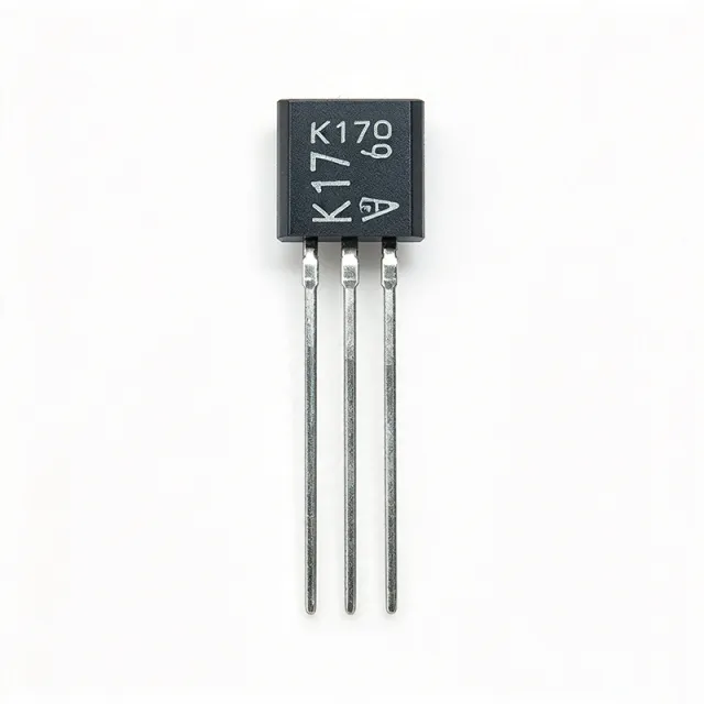
2SK170-GR - N-Channel JFET Low Noise Audio | Toshiba
The Toshiba 2SK170-GR is an N-channel silicon junction field-effect transistor (JFET) purpose-built for low-noise audio amplifier applications, supplied in a 3-pin TO-92 through-hole package. The GR grade designation identifies an Idss (zero-gate-voltage drain current) bin of 2.6 mA to 6.5 mA, the lowest-current grade in the 2SK170 family. A JFET (junction field-effect transistor) is a voltage-controlled semiconductor in which a reverse-biased gate junction controls conduction between source and drain. Unlike MOSFETs, JFETs have no insulating gate oxide, giving them very low 1/f noise and high input impedance - properties that place them at the input stage of the amplifier-device hierarchy, ahead of bipolar transistors for high-impedance, low-noise signal acquisition. The defining feature of the 2SK170-GR is its exceptionally low input-referred noise, which made it a legendary input device for audio preamplifiers, moving-magnet and moving-coil phono stages, and microphone preamps. Its high gate input impedance (in the gigaohm range typical for JFETs) allows direct connection to high-impedance sources, and its low input capacitance preserves high-frequency response in MM cartridge inputs. The GR grade is specifically chosen when the design bias point targets the 2.6-6.5 mA Idss range; designers typically select and match devices within a grade to minimize offset and distortion in differential input pairs. Because it is depletion-mode, the device conducts at Vgs = 0 and is biased with a negative gate-source voltage, simplifying self-bias circuits with a source resistor. Typical applications include discrete audio preamplifier input stages, phono equalizer front ends, condenser microphone buffers, and low-noise measurement front ends. Toshiba has discontinued the 2SK170 family, so the part is commonly sourced as leftover stock or replaced by the Linear Systems LSK170 series. Design tip: because Idss varies widely unit-to-unit, always measure and match Idss across input pairs and set bias at roughly half of Idss for best linearity and noise trade-off. This page synthesizes distributor pricing, verified drop-in alternatives, and practical matching guidance not found in the manufacturer datasheet.

2STF2220 - 1.5A PNP Power Transistor, 20V, SOT-89 | STMicroelectronics
The STMicroelectronics 2STF2220 is a PNP bipolar junction transistor (BJT) manufactured using the proprietary PB-HDC (Power Bipolar High Density Current) technology, delivering exceptional DC current gain combined with very low saturation voltage. Housed in a SOT-89-3 surface-mount package, the 2STF2220 supports a continuous collector current of up to 1.5 A and a collector-emitter breakdown voltage of 20 V, with a maximum power dissipation of 1.4 W. These characteristics make it a versatile high-gain, low-voltage PNP switch for compact, thermally efficient designs. A PNP bipolar transistor is a type of BJT where the base-emitter junction is forward-biased when the base is pulled below the emitter voltage, allowing current to flow from emitter to collector. PNP transistors complement their NPN counterparts and are commonly used in high-side switching, current mirroring, push-pull output stages, and analog signal inversion. The SOT-89-3 package family sits in the discrete semiconductors -> transistors category hierarchy, providing a compact SMD footprint with a thermal pad that improves heat dissipation relative to smaller SOT-23 housings. The 2STF2220 exhibits a DC current gain (hFE) ranging from 200 to 600, allowing reliable switching with very low base drive currents. Its collector-emitter saturation voltage is specified at low millivolt levels under moderate loads, reducing conduction losses and improving efficiency in linear regulators and load switches. The transition frequency of at least 100 MHz supports use in moderate-bandwidth amplifier and switching applications. The combination of high gain and low VCE(sat) simplifies driver design, reducing the need for complex base-drive circuitry. The PB-HDC process technology optimizes the trade-off between current-handling capability and on-state losses, enabling the 2STF2220 to replace larger PNP devices in space-constrained designs. The SOT-89-3 footprint includes a metal tab connected to the collector, which serves as a thermal pad and must be soldered to a copper pour for rated performance. This design philosophy makes the 2STF2220 suitable for portable power management, battery protection circuits, and load switching subsystems. Typical applications include power management in portable and battery-powered devices, low-side/high-side load switching, DC-DC converter peripheral circuits, MOSFET gate drivers, signal amplification in audio front-ends, LED driving stages, and complementary push-pull output stages paired with an NPN device such as the 2STF1360. When designing with this transistor, ensure the collector pad of the SOT-89-3 package is soldered to an adequate copper area to achieve rated thermal performance. Provide a base resistor to limit inrush during turn-on, and respect the maximum emitter-base voltage of 5 V to prevent reverse breakdown of the base-emitter junction. This page synthesizes distributor pricing, drop-in alternative candidates, and practical PCB thermal guidance not found in the standalone manufacturer datasheet, helping engineers quickly evaluate the 2STF2220 for both new designs and replacement scenarios.
2STR2215 - PNP High Current Density Power Transistor | ST
The STMicroelectronics 2STR2215 (sold under part reference 215) is a low-voltage fast-switching PNP power transistor manufactured using ST's proprietary PB-HCD (Power Bipolar High Current Density) technology. According to the STMicroelectronics datasheet, this technology delivers exceptional high-gain performance coupled with very low saturation voltage, making the device well suited for switching and linear power stages where conduction losses must be minimized. A PNP power transistor is a bipolar junction transistor (BJT) in which the majority current is carried by holes; it is turned on by pulling the base below the emitter potential. In the power-management hierarchy, power BJTs sit alongside MOSFETs and IGBTs as discrete power semiconductors, and PNP types are frequently paired with complementary NPN devices in push-pull outputs, linear regulators, motor drivers, and general-purpose switching circuits. The defining characteristics of the 2STR2215 are its high current gain, which reduces base-drive requirements and simplifies driver circuitry, and its very low collector-emitter saturation voltage, which reduces on-state power dissipation and improves overall efficiency in switch-mode and low-voltage applications. The fast-switching classification also makes it suitable for applications requiring quick turn-on and turn-off transitions. The complementary NPN device is the 2STR1215, allowing designers to build matched push-pull or half-bridge stages with symmetric gain and saturation characteristics. This complementary pairing simplifies thermal and electrical matching in class-AB output stages and driver applications. Typical applications include low-voltage switching regulators, power-supply output stages, motor and actuator drivers, and general-purpose amplification where a robust PNP device with low VCE(sat) is required. When designing with the 2STR2215, verify the safe operating area against the actual load current and supply voltage, and ensure adequate base-drive current to keep the device in saturation under worst-case load conditions, since insufficient drive raises VCE(sat) and junction temperature. This page synthesizes verified datasheet information, sourcing guidance, and drop-in alternative analysis not consolidated in the manufacturer datasheet.

ADTC144ECAQ-7 - NPN Pre-Biased BJT, 50V, 100mA, SOT-23 | Diodes Inc
The Diodes Incorporated ADTC144ECAQ-7 is an NPN pre-biased bipolar junction transistor (BJT) housed in a 3-pin SOT-23 surface-mount package, integrating two 47 kΩ bias resistors (R1 = R2) on a single epitaxial planar die. According to the manufacturer datasheet, the device is rated for a collector-emitter voltage of 50 V, continuous collector current of 100 mA, transition frequency of 250 MHz, and total power dissipation of 310 mW, making it suitable for switching and amplification circuits where space and component count are at a premium. A digital transistor (also known as a pre-biased transistor or resistor-equipped transistor, RET) is a BJT with integrated base and base-emitter resistors that replaces a discrete BJT plus two external bias resistors. It belongs to the broader transistor family (BJT > semiconductor > active electronic component). By collapsing three discrete parts into one SOT-23, digital transistors simplify PCB layout, lower BOM count, reduce parasitic inductance, and enable direct logic-level drive from microcontrollers without external bias networks. Key features include built-in 47 kΩ / 47 kΩ bias resistors (R1 = R2), eliminating the need for external base biasing; an epitaxial planar die construction that improves switching performance and minimizes leakage; and AEC-Q101 qualification that makes the part suitable for automotive applications requiring specific change control. The part is also PPAP capable and manufactured in IATF 16949 certified facilities, with totally lead-free, fully RoHS-compliant, halogen-free and antimony-free "green" device construction. Architecturally, the ADTC144ECAQ-7 uses a standard NPN epitaxial planar BJT die with monolithic resistor integration. The 47 kΩ / 47 kΩ ratio means the device is biased to switch on when its input voltage exceeds roughly 0.7 V plus the drop across the bias network, allowing direct interface to 1.8 V, 3.3 V, or 5 V logic. The 250 MHz transition frequency supports medium-speed switching applications including level shifting, interface buffering, and relay/LED driver circuits. Typical applications include digital logic interfacing, MOSFET gate drivers, relay and solenoid drivers, LED indicator drivers, level shifters between logic domains, and inverter stages in automotive body electronics, white goods, and industrial control boards. The automotive-grade qualification broadens use to BCMs, HVAC controls, and instrument cluster signal conditioning. When designing with the ADTC144ECAQ-7, observe the 310 mW power dissipation ceiling, derate above 25 °C ambient, and place the device near the driven load to minimize trace inductance. This page synthesizes distributor pricing, drop-in alternatives, and practical design notes not found in the manufacturer datasheet.

ADUM3223ARWZ - 4A Isolated Half-Bridge Gate Driver | Analog Devices
The ADUM3223ARWZ is a 4 A isolated, half-bridge gate driver from Analog Devices, employing iCoupler technology to provide independent and isolated high-side and low-side outputs. It offers 3000 V rms isolation in a narrow body, 16-lead SOIC package, making it suitable for a wide range of power conversion applications. The device combines high speed CMOS and monolithic transformer technology, delivering robust performance with minimal propagation delay and excellent common-mode transient immunity. An isolated gate driver is a specialized integrated circuit that provides the necessary voltage and current to drive the gate of power transistors (such as MOSFETs and IGBTs) while maintaining galvanic isolation between the control side and the power stage. This isolation is critical in applications where the power stage operates at high voltages or in noisy environments, protecting the low-voltage control circuitry and ensuring safe, reliable operation. Isolated gate drivers are essential components in switch-mode power supplies, motor drives, and inverters, where they enable efficient and safe switching of high-power devices. Key features of the ADUM3223ARWZ include 4 A peak output current, 3000 V rms isolation, and a wide supply voltage range. The device supports both high-side and low-side outputs with independent inputs, allowing flexible control of half-bridge topologies. It also features a high common-mode transient immunity (CMTI) of typically 100 kV/us, ensuring reliable operation in noisy environments. The propagation delay is typically 50 ns, enabling high-frequency switching with minimal timing skew. Technically, the ADUM3223ARWZ integrates Analog Devices' iCoupler technology, which uses chip-scale transformers to transmit signals across the isolation barrier. This approach offers advantages over traditional optocouplers, including higher speed, lower power consumption, and better reliability. The device is designed to drive power MOSFETs and IGBTs directly, with a wide output supply range from 4.5 V to 18 V, accommodating various gate drive requirements. The narrow body SOIC-16 package is compact and suitable for space-constrained designs. Typical applications include isolated switch-mode power supplies, motor drives, solar inverters, and industrial automation. The ADUM3223ARWZ is particularly well-suited for half-bridge and full-bridge topologies where high-side and low-side drivers are required. Its high output current ensures fast switching of large gate capacitances, reducing switching losses and improving efficiency. When designing with this device, it is important to provide adequate decoupling on both the input and output supplies, and to ensure proper layout to minimize parasitic inductance. The device also requires careful consideration of the isolation rating and creepage distances for the target application's safety standards.

AIKB50N65DF5ATMA1 - 650V 50A TRENCHSTOP 5 IGBT | Infineon
The Infineon AIKB50N65DF5ATMA1 is a 650 V, 50 A automotive-grade NPT IGBT featuring TRENCHSTOP 5 technology, co-packaged with a RAPID-1 fast-recovery anti-parallel diode, in a surface-mount PG-TO263-3-2 (D2PAK) package. It is engineered for high-efficiency hard-switching and resonant topologies with best-in-class switching losses and conduction characteristics. An IGBT (Insulated-Gate Bipolar Transistor) is a power semiconductor that combines the high-input impedance of a MOSFET with the low-saturation-voltage drop of a bipolar transistor, enabling efficient switching at high voltages and currents. It sits in the power-semiconductor hierarchy alongside MOSFETs and sits downstream of gate drivers and upstream of the inductive load it commutates. IGBTs are the workhorse of mid-voltage (400 V to 1700 V), high-current (10 A to 3600 A) power conversion. Key features of the AIKB50N65DF5ATMA1 include 650 V collector-emitter breakdown voltage, 50 A nominal collector current, very low VCE(sat) for reduced conduction loss, and a co-packaged RAPID-1 soft fast-recovery diode optimized for low EMI and high dv/dt immunity. The TRENCHSTOP 5 thin-wafer technology shrinks switching losses by roughly 20 percent versus previous TRENCHSTOP generations, and the part is qualified to AEC-Q101 for automotive use. The thin-wafer TRENCHSTOP 5 cell architecture replaces the older NPT field-stop concept with a smaller die that reduces both Eon and Eoff per switching cycle. The integrated RAPID-1 diode is matched to the IGBT's switching speed, suppressing reverse-recovery spikes and lowering electromagnetic emissions in hard-switched bridges such as totem-pole PFC. Typical applications include on-board chargers for electric vehicles, automotive and industrial PFC stages, totem-pole PFC and bridgeless boost converters, DC/AC inverters for motor drives, photovoltaic string and micro-inverters, and uninterruptible power supplies. The 650 V class rating suits 400 V DC-link designs common in EV powertrains and three-phase industrial drives. When designing with this part, observe the datasheet's maximum case temperature, keep the gate-drive loop inductance below the recommended limit (typically below 20 nH) and choose a turn-off gate resistor that balances Eoff against dv/dt-induced ringing. The D2PAK footprint requires sufficient PCB copper area for thermal dissipation at full load. This page synthesizes distributor pricing, drop-in pin-compatible alternatives, and application-focused design notes not found in the standalone Infineon datasheet.
BC547BTA - 45V NPN BJT 100mA TO-92 | onsemi
The onsemi BC547BTA is an NPN bipolar junction transistor (BJT) in a TO-92-3 through-hole package with 45 V VCEO, 100 mA continuous collector current, 300 MHz transition frequency, and 500 mW power dissipation. It belongs to the BC547 series (gain group B, hFE 200-450) and is qualified for general-purpose amplifier and low-power switching applications. An NPN bipolar junction transistor (BJT) is a three-terminal semiconductor device consisting of an N-type collector, a P-type base, and an N-type emitter. BJTs are the foundational active components of analog electronics, used as small-signal amplifiers, switches, and current sources. In the wider component hierarchy, small-signal NPN BJTs like BC547 sit under discrete semiconductors > transistors > bipolar transistors > epitaxial silicon transistors, providing the gain and switching function for virtually every analog and digital control circuit. The BC547BTA features a low-noise epitaxial silicon die with a typical DC current gain (hFE) of 330 at 2 mA, making it well-suited for audio pre-amplifier input stages, sensor signal conditioning, and general-purpose switching. It provides 300 MHz transition frequency (fT) for RF and high-speed pulse applications, 5 pF typical output capacitance, and a 5 ns storage time for fast switching. The TO-92-3 package with formed leads supports automatic insertion and is the de-facto industry standard for through-hole small-signal transistors. The BC547BTA's PNP complement is the BC557, which shares the same TO-92 package and gain group nomenclature. The 'B' suffix designates the hFE bin (200-450), distinguishing it from BC547A (110-220) and BC547C (420-800). Designers typically select the BC547B as a balance between gain and stability for audio and general-purpose circuits. Typical applications include audio pre-amplifiers, signal conditioning for sensors, general-purpose switching interfaces for microcontrollers, RF amplifier stages up to 300 MHz, oscillator circuits, and Darlington-pair drivers. The through-hole TO-92 package also makes it a popular choice for prototyping, education labs, and hobbyist projects. When designing with the BC547BTA, ensure the collector current remains below 100 mA continuous and the junction temperature stays within -55C to +150C. Use a base resistor to limit base current and prevent excessive collector current, and add a flyback diode when driving inductive loads to protect against reverse-EMF. This page synthesizes distributor pricing from DigiKey/Mouser, drop-in alternatives from the BC547/2N3904 family, and practical design notes not found on a single manufacturer datasheet, providing engineers with a complete sourcing and design reference in one place.