Produits (39 000+)

MC56F8322MFAE - 60MHz 56800E DSC, 32KB Flash | NXP LQFP-48
MC56F8322MFAE

MC56F8322MFAE - 60MHz 56800E DSC, 32KB Flash | NXP LQFP-48

The NXP MC56F8322MFAE is a 16-bit digital signal controller from the 56800E core family, delivering up to 60 MIPS at 60 MHz core frequency with 32 KB of on-chip Flash memory and a comprehensive peripheral set, housed in a 48-pin LQFP (7x7 mm) package. This hybrid DSP+MCU device combines the processing throughput of a digital signal processor with the peripheral integration and C-friendly programming model of a microcontroller. A digital signal controller (DSC) is a hybrid processor category that sits between a microcontroller (MCU) and a digital signal processor (DSP) in the embedded-semiconductor hierarchy: MCU -> DSC -> DSP -> processor. DSCs typically use a Harvard-style architecture with parallel execution units, deterministic interrupt response, single-cycle MAC, and integrated analog peripherals, targeting real-time control loops such as motor drives, power conversion, and audio processing. Key features include 32 KB (16K x 16) of Flash program memory, up to 60 MIPS sustained throughput at 60 MHz, a 56800E Harvard-style core with three parallel execution units capable of six operations per instruction cycle, and an instruction set optimized for both DSP and control code. The 48-LQFP device integrates peripherals including CAN, SCI, SPI, ADC, PWM, and GPIOs. Operating voltage is 2.5 V core / 3.3 V I/O. The 56800E core combines DSP-class MAC and barrel-shifter resources with MCU-style peripheral and interrupt handling, allowing efficient C compilation while still sustaining real-time DSP loops. The Harvard architecture with separate program and data buses enables deterministic single-cycle instruction fetch and dual operand reads, which is critical for tight digital control loops. Typical applications include digital motor control (BLDC, PMSM, stepper), AC/DC and DC/DC power conversion, uninterruptible power supplies, audio processing, and industrial automation. The CAN interface plus PWM outputs make this DSC especially suited to automotive and industrial control nodes. When designing with this device, allocate a minimum 2.5 V regulated rail with adequate decoupling (4.7 µF + 0.1 µF) close to the VDD pins, and follow the recommended oscillator startup delay sequence to avoid Flash corruption during boot. This page synthesizes distributor stock and pricing, AEC-Q100 automotive temperature grade details, and drop-in alternative guidance not found in the standalone manufacturer datasheet, helping engineers shorten sourcing and qualification cycles.

Devis Contact
MC56F8335MFGE - 16-bit 60MHz DSC, 64KB Flash, 128-LQFP | NXP
MC56F8335MFGE

MC56F8335MFGE - 16-bit 60MHz DSC, 64KB Flash, 128-LQFP | NXP

The NXP MC56F8335MFGE is a 16-bit Digital Signal Controller (DSC) from the 56800E core-based family, integrating digital signal processing and microcontroller functionality on a single chip. It operates at 60 MHz, integrates 64 KB (32K x 16) of program Flash, and is housed in a 128-pin LQFP package (14 x 20 mm). Per NXP's product page, the part is flagged NRND (Not Recommended for New Designs), so designers should plan migration paths or evaluate the alternatives listed below. A Digital Signal Controller (DSC) is a hybrid device that combines the deterministic control of a microcontroller (MCU) with the mathematical throughput of a digital signal processor (DSP). Within the broader taxonomy, a DSC sits between microcontrollers (control-oriented) and DSPs (math-oriented), and is itself a member of the larger microcontroller and embedded-processor IC family. The 56800E core extends this hybrid concept with a Harvard-style architecture, hardware DO-loop, and single-cycle MAC, making the MC56F8335MFGE suitable for both control loops and real-time signal conditioning in a single device. Key features of the MC56F8335MFGE include 64 KB (32K x 16) Flash program memory, on-chip RAM, 49 general-purpose I/O, and a rich peripheral set: CANbus, EBI/EMI, two SCIs, one SPI, PWM, a temperature sensor, a watchdog timer, and power-on reset. The 56800E core delivers 60 MIPS with hardware MAC, accelerating closed-loop control and DSP-style filtering without offloading to a separate DSP. Connectivity options include CAN, SCI, and SPI, which is typical for industrial motor-control and sensor-interface boards. Typical applications for the MC56F8335MFGE include digital motor control (BLDC, PMSM, AC induction), industrial inverters, uninterruptible power supplies, smart sensors, and automotive body electronics. The combination of PWM, CAN, ADC, and the 56800E MAC makes the device particularly well suited to Field-Oriented Control (FOC) of three-phase motors and to power-conversion control loops where deterministic interrupt latency matters. When designing with this device, verify operating temperature grade from the device datasheet suffix, ensure PCB layout accommodates the 14 x 20 mm 128-LQFP footprint, and plan for a migration to the active 56F83xx successor because the MPN is NRND. Designers should evaluate pin-compatible family variants before committing to a long-lifecycle BOM.

Devis Contact
MC56F8345MFGE - 16-bit DSC 56800E 60MHz 128KB Flash | NXP
MC56F8345MFGE

MC56F8345MFGE - 16-bit DSC 56800E 60MHz 128KB Flash | NXP

The NXP Semiconductors MC56F8345MFGE is a 16-bit digital signal controller (DSC) based on the 56800E core, operating at up to 60 MHz with 128KB (64K x 16) of on-chip Flash program memory, housed in a 128-pin LQFP (14 x 20 mm) package. As part of the 56F834X/56F814X family, it combines the computational throughput of a DSP with the peripheral integration and control flexibility of a microcontroller. A digital signal controller is a hybrid processor class that sits between a general-purpose microcontroller (MCU) and a dedicated digital signal processor (DSP). DSCs such as the 56800E-family parts execute multiply-accumulate (MAC)-intensive DSP algorithms while retaining MCU-style peripherals, interrupt handling, and C-code programmability, making them the natural choice at the top of the embedded control hierarchy for real-time closed-loop systems. Key features of the MC56F8345MFGE include the 16-bit 56800E hybrid core with dual Harvard architecture for parallel instruction and data fetch, 128KB Flash program memory and on-chip RAM, a 12-bit analog-to-digital converter supporting simultaneous motor-control feedback sampling, and multiple pulse-width modulation (PWM) outputs purpose-built for inverter and power-conversion control. Its automotive-relevant temperature grade and gull-wing LQFP terminations support reliable surface-mount assembly. Technically, the 56800E core achieves single-cycle 16 x 16 MAC operations and executes DSP-style bit-manipulation instructions, allowing one controller to run field-oriented motor control loops alongside housekeeping tasks. Program Flash is executable in place, and the peripheral set (PWM, ADC, timers, serial interfaces) is tightly coupled to the core for low-latency control interrupts. Typical applications include three-phase brushless DC (BLDC) and permanent-magnet synchronous motor (PMSM) drives, industrial power conversion (inverters, converters, UPS), and digital power supplies where fast deterministic control loops at 60 MHz are essential. When designing with this device, verify availability early: NXP lists this part as NRND (Not Recommended for New Designs), so new projects should evaluate the recommended successor family, and existing designs should secure last-time-buy inventory. This page synthesizes distributor pricing context, drop-in alternatives, and practical design guidance not found in the manufacturer datasheet.

Devis Contact
MC56F8346MFVE - 16-Bit 60MHz DSC | NXP | Motor Control
MC56F8346MFVE

MC56F8346MFVE - 16-Bit 60MHz DSC | NXP | Motor Control

The NXP Semiconductors MC56F8346MFVE is a 16-bit digital signal controller with a 56800E core, 60 MHz processing capability, 128 KB of flash memory, and a 144-LQFP package. The DigiKey listing identifies the device as a 3.3 V, 16-bit microcontroller/DSC in a 20 mm × 20 mm LQFP package. Its combination of embedded control, signal processing, and enhanced PWM makes it relevant to motor-control and power-conversion systems. A digital signal controller, or DSC, combines a microcontroller’s peripheral integration and deterministic control capabilities with a processor designed for demanding signal-processing work. The 56800E architecture sits between a general-purpose microcontroller and a digital signal processor: it supports embedded software control while adding processing capability for algorithms that benefit from a dedicated DSP core. This places the MC56F8346MFVE in the broader semiconductor and embedded-control hierarchy. Verified listing information highlights a 60 MHz clock, 128 KB flash organized as 64K × 16, 16-bit architecture, 144 leads, and surface-mount construction. The NXP cross-reference snippet also describes enhanced PWM for motor control and power-conversion applications. These are meaningful selection criteria because PWM resolution and update behavior directly influence current-loop and switching-control performance. The device is intended for embedded motor-control and power-conversion designs rather than general-purpose computing. Suitable implementation areas include digital motor controllers, inverter control, power-factor correction, and switching power supplies where deterministic control, fast peripheral access, and PWM generation are important. The exact peripheral configuration and memory behavior must be confirmed against the NXP manufacturer datasheet before design release. Designers should review the LQFP-144 pinout, exposed-pad handling, clocking, power supplies, decoupling, and unused-pin requirements directly from the manufacturer documentation. Because the NXP product page labels the component as End of Life, procurement planning should include lifecycle verification, approved sourcing, and a review of available inventory rather than assuming long-term production support. This page combines the verified manufacturer identification, distributor catalog data, lifecycle indication, and application-level engineering context. It also distinguishes catalog-confirmed facts from parameters requiring confirmation from the full datasheet, helping engineers plan replacement and redesign decisions without confusing similar 56F8xxx devices with verified drop-in alternatives.

Devis Contact
MC56F8346VFVE - 16-Bit 60MHz 128KB Flash DSC | NXP LQFP-144
MC56F8346VFVE

MC56F8346VFVE - 16-Bit 60MHz 128KB Flash DSC | NXP LQFP-144

The NXP MC56F8346VFVE is a 16-bit hybrid digital signal controller (DSC) based on the 56800E core, integrating DSP processing power and microcontroller functionality on a single chip. It operates at 60 MHz, includes 128 KB (64K x 16) of on-chip flash program memory, and is packaged in a 144-pin LQFP (20 x 20 mm). A Digital Signal Controller (DSC) is a hybrid device class that merges the deterministic math engine of a digital signal processor (DSP) with the peripheral set, interrupt model, and C-friendly toolchain of a microcontroller. Within the power management and embedded control taxonomy, the 56F8xxx family sits between conventional 16-bit microcontrollers and full 32-bit DSPs, offering single-cycle MAC, hardware DO loops, and bit-reversed addressing while retaining byte-level peripheral control. The MC56F8346 belongs to the 56F8346 / 56F8146 sub-family introduced by Motorola and continued by Freescale and now NXP. Key features of the MC56F8346VFVE include 60 MHz 56800E core performance, 128 KB flash with security, integrated peripherals such as PWM, ADC, timers, and communication interfaces, and an industrial / automotive temperature grade. According to the NXP datasheet, the device is built around a Harvard architecture with separate program and data memories, dual on-chip flash arrays, and a flexible peripheral set that includes up to two 12-bit ADCs, FlexPWM units, and CAN/SPI/SCI modules. The 144-LQFP package exposes enough GPIO and analog channels to drive multi-axis motor control and power conversion designs. Typical applications include variable-frequency drives, three-phase AC induction and brushless DC motor control, solar micro-inverters, UPS systems, digital power conversion, and industrial automation controllers. Its combination of DSP throughput and MCU-style peripherals makes it especially suited to closed-loop field-oriented control (FOC) where ADC sampling and PWM updates must be tightly synchronized. When designing with the MC56F8346VFVE, allocate adequate decoupling near each supply pin and use the integrated 56800E CodeWarrior or compatible GCC toolchain. Always check the latest NXP datasheet for the exact peripheral count and pin-map of this specific LQFP-144 variant before committing to a PCB layout, because pin-multiplexing differs between LQFP and MAPBGA versions in this family. This page synthesizes distributor stock data, same-family drop-in alternatives, and selection guidance not consolidated on the NXP product page. Verified against DigiKey and Mouser listings as of 2026-10-19.

Devis Contact
MC56F8346VFVER2 - 16-Bit 60MHz DSC, 128KB Flash | NXP
MC56F8346VFVER2

MC56F8346VFVER2 - 16-Bit 60MHz DSC, 128KB Flash | NXP

The NXP MC56F8346VFVER2 is a 16-bit digital signal controller (DSC) from the 56800E core-based 56F8xxx family, delivering 60 MIPS at 60 MHz with 128 KB of program Flash memory in a 144-pin LQFP (20x20 mm) package. It integrates peripheral modules tailored for embedded motor, power conversion, and digital signal processing tasks, including four 12-bit ADCs supporting simultaneous conversions with quad 4-pin multiplexed inputs, plus PWM and timer channels synchronized for motor-control loops. Operating from a 3.3 V supply, the device combines the deterministic interrupt behavior of a microcontroller with the math throughput of a DSP engine on a single chip. A digital signal controller (DSC) is a hybrid MCU/DSP architecture that fuses a C-programmable microcontroller core with DSP-class multiply-accumulate (MAC) units and single-cycle arithmetic logic. In the system hierarchy it sits above general-purpose microcontrollers and below dedicated DSPs, bridging deterministic control loops (typical of MCUs) with high-throughput signal processing (typical of DSPs). The 56800E core also exposes Harvard-style bus structures and on-chip program/data memory, so firmware can run from internal Flash without external bus glue. Key features include 128 KB of Flash, 12 KB of unified RAM, two 4-channel Quadrature Decoders supporting encoder feedback from brushless motors, multiple serial communication interfaces (SCI, SPI, I2C), a CAN 2.0 B controller, four 12-bit ADCs, and up to 62 GPIO. The 144-LQFP footprint exposes all peripheral pins while supporting industrial temperature operation (-40 °C to +105 °C minimum), sufficing harsh-environment deployments with thermal headroom typical of motor-drive enclosures. Application highlights include industrial variable-frequency drives, digital servo amplifiers, uninterruptible power supplies (UPS), photovoltaic inverters, smart appliance motor control, and precision instrumentation. Engineers typically choose this DSC when deterministic PWM timing plus low-latency ADC sampling is required for closed-loop control. Design should observe the datasheet's reference decoupling, ground-plane, and unused-pin tie-offs to ensure ADC and PWM noise immunity in mixed-signal layouts.

Devis Contact
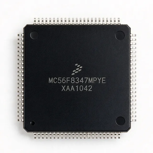
MC56F8347MPYE - 16-Bit DSC 60MHz 128KB Flash 160-LQFP | NXP
MC56F8347MPYE

MC56F8347MPYE - 16-Bit DSC 60MHz 128KB Flash 160-LQFP | NXP

The NXP MC56F8347MPYE is a 16-bit hybrid Digital Signal Controller (DSC) from the 56800E 56F8xxx family, featuring a 60 MHz 56800E core, 128 KB (64K x 16) of program flash memory, and a 160-pin LQFP (24x24 mm) package. It integrates a microcontroller's control peripherals with a DSP's computational engine, targeting motor control, power conversion, and embedded motion-control applications. A Digital Signal Controller (DSC) is a hybrid architecture that combines the deterministic interrupt response and on-chip peripherals of a microcontroller (MCU) with the multiply-accumulate (MAC) throughput and single-cycle hardware math capabilities of a Digital Signal Processor (DSP). In the broader taxonomy, the 56800E core places this device between fixed-point DSPs (like the DSP56800) and 32-bit general-purpose MCUs (like the Kinetis E series), making it part of the Freescale/NXP legacy 16-bit DSC portfolio. The 56F8xxx family is widely used in cost-sensitive industrial and consumer motor control where the 60 MHz throughput exceeds ARM Cortex-M0 capability but full DSP architectures (TI C2000) are over-spec. Key differentiating features include 128 KB of on-chip flash for application code and parameter tables, on-chip EEPROM/flash for data storage, dual 12-bit (or 10-bit on some variants) analog-to-digital converters (ADCs) with programmable gain amplifiers (PGAs), enhanced PWM modules with fault inputs for three-phase motor drive, quadrature decoders, CAN, SPI, I2C, and JTAG/OnCE debug interfaces. The 160-LQFP package provides ample GPIO and ADC channel count for multi-axis or multi-phase applications. The 56800E core executes instructions from a unified program flash with hardware MAC and barrel shifter, supports Harvard-style simultaneous fetch, and provides single-cycle 16x16 MAC plus 32-bit accumulator operations. The bus architecture includes a peripheral bridge to slow-speed peripherals and supports DMA-mapped data movement, leaving the core free for control-loop closure. Typical applications include variable-frequency motor drives (BLDC, PMSM, ACIM), three-phase uninterruptible power supplies (UPS), digital PFC stages, servo amplifiers, and appliance control boards. The enhanced PWM (eFlexPWM) modules with submodules, complementary outputs, and hardware dead-time generation are particularly suited to three-phase inverter switching. When designing with this device, reserve the largest package variant for migrations to higher-memory devices in the same family; verify the bonded-out pin map for ADC channel count before committing the PCB, since some derivatives expose fewer ADC inputs to free PWM/quadrature pins. Plan the JTAG chain for in-system programming and OnCE debug access during development.

USD $16,41 En stock
MC56F8347VPY60 - 60MHz 16-bit DSC, 128KB Flash | NXP | 160-LFQFP
MC56F8347VPY60

MC56F8347VPY60 - 60MHz 16-bit DSC, 128KB Flash | NXP | 160-LFQFP

The NXP (formerly Freescale) MC56F8347VPY60 is a 16-bit Digital Signal Controller (DSC) combining the peripheral set and ease-of-use of an MCU with the computational power and throughput of a DSP, operating at 60 MHz with 128 KB of on-chip program Flash and 160 pins in an LQFP-160 (LFQFP) industrial-grade package. The MC56F8347VPY60 is built on the 56800E core family and integrates peripherals tuned for digital motor control, power conversion, and embedded signal processing applications, delivering up to 60 MIPS of deterministic throughput for closed-loop control loops. A Digital Signal Controller is a hybrid class of embedded processor that fuses a microcontroller's deterministic interrupt-driven peripheral set with a digital signal processor's single-cycle MAC (multiply-accumulate) engine and parallel data paths. DSCs sit in the hierarchy between general-purpose microcontrollers (which lack DSP throughput) and standalone DSPs (which lack on-chip analog/control peripherals), making them the de-facto choice for digital motor control, switched-mode power supplies, sensor signal conditioning, and high-speed instrumentation. The 56F83xx family specifically targets embedded real-time control where deterministic latency, on-chip ADCs/PWMs, and DSP-grade math are required in a single chip. Key features include a 60 MHz 56800E Harvard-architecture core with single-cycle 16-bit x 16-bit MAC, 128 KB of program Flash, 8 KB of unified data/program RAM, dual 12-bit ADCs with 1.5 us conversion time, a 6-channel PWM module with programmable dead-time insertion, a Quadrature Decoder, multiple serial interfaces (SCI, SPI, I2C), a 4-channel DMA controller, and an external memory interface to LQFP-160 packages with up to 76 general-purpose I/O pins. The 'VPY' package suffix indicates the 160-pin LFQFP industrial-temperature grade (-40C to +105C), and the '60' suffix denotes 60 MHz operation. The 56800E core implements a modified Harvard architecture with three execution units operating in parallel: an Address Generation Unit (AGU), a Data Arithmetic Logic Unit (DALU), and a Program Controller. The single-cycle MAC engine delivers up to 60 MIPS of signal-processing throughput, while the on-chip dual 12-bit ADC samples at up to 1.5 us per conversion enabling precise current/voltage sensing in motor control loops. The on-chip regulator and brown-out detector enhance robustness for industrial environments. Typical applications include AC induction motor vector control, permanent-magnet synchronous motor (PMSM) field-oriented control (FOC), digital PFC power factor correction, uninterruptible power supplies (UPS), solar micro-inverters, three-phase UPS systems, industrial servo drives, and sensor signal processing instrumentation. The dual ADC with simultaneous sampling enables field-oriented control current loops at switching frequencies up to 50 kHz without external ADC support. When designing with this device, carefully plan PCB thermal dissipation: at 60 MHz the core dissipates approximately 0.5 W, and the LFQFP-160 package requires at least 25 cm^2 of 2 oz copper pour for adequate cooling. Designers should also validate toolchain compatibility with CodeWarrior IDE or the Processor Expert tool suite, as the 56800E core requires the legacy 56F8xxx SDK for peripheral drivers and the CW56800 compiler for the C/C++ source. This page synthesizes distributor pricing, drop-in alternatives, and practical design notes not found in the manufacturer datasheet.

Devis Contact
MC56F8347VVFE - 16-Bit 60MHz DSP MCU, 128KB Flash, 160-MAPBGA | NXP
MC56F8347VVFE

MC56F8347VVFE - 16-Bit 60MHz DSP MCU, 128KB Flash, 160-MAPBGA | NXP

The NXP (formerly Freescale) MC56F8347VVFE is a 16-bit Digital Signal Controller from the 56F8300 family that combines microcontroller (MCU) integration with digital signal processing (DSP) throughput. Housed in a 160-pin MAPBGA package (15x15 mm), it integrates a 56800E core running up to 60 MHz, 128 KB of on-chip Flash program memory (64K x 16), and 12 KB of unified data/parameter RAM (6K x 16). The device also provides 76 general-purpose I/O lines plus dedicated peripheral pins, supporting mixed analog and digital mixed-signal designs. A Digital Signal Controller (DSC) sits in the hierarchy between a microcontroller and a full DSP: like an MCU it integrates Flash, RAM, timers, ADC, and communication peripherals on-chip; like a DSP it offers single-cycle MAC, Harvard-style bus architecture, and deterministic interrupt latency. DSCs are used where the application requires DSP-class signal processing throughput (motor control loops, power-conversion algorithms, audio/voice processing) without the cost and complexity of a separate DSP + MCU pair. Key features include an on-chip enhanced Synchronous Serial Interface (SSI) and Serial Peripheral Interface (SPI), dual SCI (UART) ports, a 12-bit ADC with up to 8 input channels, a Quad Timer module, PWM outputs suitable for motor drive, and a JTAG/OnCE debug port. The 56800E core executes most instructions in a single clock cycle and supports hardware DO/REP loops, making it well-suited to fixed-point control and signal processing tasks. Architecturally, the 56F8347 separates program Flash (128 KB) and data Flash (up to 8 KB optional) from unified RAM, allowing concurrent instruction fetch and data access through dual on-chip buses. The integrated peripherals share a peripheral interrupt controller with configurable priorities. Operating voltage is typically 3.0 V to 3.6 V, with industrial temperature grade options. Typical applications include variable-frequency motor drives (BLDC, PMSM, ACIM), digital power conversion (UPS, solar inverters, SMPS), industrial automation controllers, smart sensor signal conditioning, and consumer audio processing. The combination of DSP throughput and MCU-style integration reduces BOM cost in motor-control designs. When designing with the MC56F8347VVFE, ensure the MAPBGA PCB footprint includes 4-layer construction with via-in-pad or micro-vias, as the 0.8 mm pitch BGA cannot be hand-soldered. The on-chip voltage regulator and decoupling requirements are detailed in the MC56F8347 datasheet; inadequate decoupling causes Flash programming failures during in-field updates. This page synthesizes distributor pricing, package data, and practical design notes for the MC56F8347VVFE not found in the manufacturer datasheet alone.

Devis Contact
MC56F8355MFGE - 16-bit 60MHz DSC 256KB Flash | NXP
MC56F8355MFGE

MC56F8355MFGE - 16-bit 60MHz DSC 256KB Flash | NXP

The NXP MC56F8355MFGE is a 16-bit digital signal controller (DSC) based on the 56800E core, running at 60 MHz with 256 KB (128K x 16) of on-chip flash program memory, housed in a 128-pin LQFP (14x20 mm) package. A digital signal controller combines the computational architecture of a digital signal processor (DSP) with the peripheral set and control structure of a microcontroller. In the product hierarchy, the MC56F8355MFGE sits within NXP's 56800E core-based DSC family, under digital signal controllers, under hybrid microcontrollers, and under the broader semiconductor/IC category. This hybrid architecture allows a single chip to execute both tight real-time signal-processing loops and general control firmware. Key features include a 16-bit 56800E core at 60 MHz, 256 KB flash, dual 12-bit ADC converters for simultaneous sampling, and integration of CAN, SCI, and SPI serial interfaces with 49 general-purpose I/O lines. The dual ADCs are significant for motor control because phase currents on multiple legs can be sampled at precisely the same instant. Technically, the 56800E core blends Harvard-architecture DSP execution (single-cycle MAC, hardware looping, bit-reversed addressing) with a conventional MCU programming model, supported by the NXP CodeWarrior development environment and the Processor Expert configuration tool. The 56F835X/815X family members share a common peripheral set and documentation, easing migration between memory densities. Typical applications are high-precision motor control (BLDC, PMSM, AC induction with FOC), digital power conversion such as switched-mode power supplies and inverters, and industrial automation nodes requiring deterministic real-time control. Per NXP, the device enables high-precision motor control with 60 MHz performance and dual 12-bit ADCs. Design consideration: the device operates from 2.25 V to 3.6 V over -40 C to +125 C, so 5 V sensor signals need level shifting, and flash retention and Vcap pin requirements documented in the datasheet must be honored. This page synthesizes distributor pricing, family drop-in alternatives, and practical design notes not found in the manufacturer datasheet.

Devis Contact
MC56F8355VFGE - 16-Bit 60MHz DSC 256KB Flash LQFP-128 | NXP
MC56F8355VFGE

MC56F8355VFGE - 16-Bit 60MHz DSC 256KB Flash LQFP-128 | NXP

The NXP Semiconductors MC56F8355VFGE is a 16-bit digital signal controller (DSC) from the 56800E core-based 56F835x/56F815x family, integrating 256KB of on-chip Flash program memory and operating at 60MHz core speed. Housed in a 128-pin LQFP (14x20 mm) package, the device combines microcontroller (MCU) peripherals with DSP-class processing throughput on a single die. This hybrid architecture positions the part as a "DSC" - a class of mixed-signal controllers that sit between traditional 8/16/16-bit MCUs and higher-end DSPs in the embedded-processing taxonomy. A digital signal controller is an integrated circuit category that fuses a deterministic microcontroller (MCU) with DSP-oriented multiply-accumulate (MAC) and Harvard-bus execution units. DSCs belong to the broader microprocessor hierarchy: microcontroller -> digital signal controller -> digital signal processor (DSP) -> embedded processor -> semiconductor. They are commonly used in real-time control loops where both fast arithmetic and event-driven peripheral handling are required. Key feature highlights of the MC56F8355VFGE include 256KB (128K x 16) of Flash program memory, 49 general-purpose I/O pins, and connectivity peripherals spanning CANbus, EBI/EMI, SCI, and SPI. The integrated peripheral set further includes Power-On Reset (POR), Pulse-Width Modulation (PWM) modules, a temperature sensor, and a Watchdog Timer (WDT). These blocks support closed-loop motor control, power conversion, and sensor-fusion applications without external companions. At the silicon level, the 56800E core uses a dual Harvard architecture with on-chip instruction and data memories, supporting single-cycle 16x16-bit MAC operations. Operating from a 3.3V supply, the device is fabricated on a CMOS process and is intended for industrial temperature environments. The instruction set, JTAG/OnCE debug interface, and integrated analog peripherals reduce external BOM cost in motor drive and digital-power designs. Typical applications include AC induction motor and BLDC motor control (variable-frequency drives, servo drives), digital power conversion (SMPS, PFC stages), industrial automation, automotive body and chassis subsystems, and uninterruptible power supplies. The combination of PWM timers, ADC-triggered sequencing, and CAN/SPI connectivity suits distributed real-time nodes. Designers should evaluate the 60MHz throughput, Flash wait-state budget, and ADC sampling latency against target loop rates. Use the on-chip PWM fault inputs and the watchdog timer to meet functional-safety requirements in motor drives. Verify thermal rise on the LQFP-128 footprint with sufficient copper area. This page synthesizes distributor pricing, drop-in compatible 56F8xxx variants, and practical PCB-layout guidance that is not found in the manufacturer datasheet alone.

Devis Contact
MC56F8356MFV60 - 60MHz 16-bit DSC, 144-pin LQFP | NXP
MC56F8356MFV60

MC56F8356MFV60 - 60MHz 16-bit DSC, 144-pin LQFP | NXP

The NXP MC56F8356MFV60 is a 60 MHz 16-bit hybrid Digital Signal Controller (DSC) from the 56F8300 family, integrating the 56800E core with DSP and MCU functionality on a single die, delivered in a 144-pin LQFP package with 1 DSP engine and 256 KB of program Flash. According to the Freescale/NXP 56F8356/56F8156 Technical Data document, the device includes 4 KB unified RAM, 8 KB data Flash, dual 12-bit ADCs, FlexPWMs, FlexCAN, and an external memory interface, enabling migration paths from the 56F8346 with minimal hardware changes. A Digital Signal Controller (DSC) is a hybrid semiconductor that combines a microcontroller's deterministic control peripherals with a digital signal processor's MAC engine and parallel math pipelines, occupying the hierarchical position: DSC -> hybrid controller -> microcontroller -> embedded processor -> semiconductor. Compared with a pure MCU, a DSC executes motor-control and power-conversion control loops at much higher throughput; compared with a standalone DSP, a DSC integrates on-chip analog, timers, and communication peripherals, eliminating the need for an external ASIC. Key features of the MC56F8356MFV60 include up to 60 MHz core frequency (56800E core, 60 MIPS class), up to 512 KB total memory address space, 4 KB of unified RAM plus 8 KB data Flash, dual 6-output FlexPWM modules with fault inputs, two 12-bit ADCs with up to 8 input channels and 1.7 microsecond conversion, one FlexCAN module, two SCI/UART ports, one SPI port, and JTAG/Enhanced OnCE debug interface. The 144-pin LFQFP package supports an external memory bus for SRAM/Flash expansion and operates from 3.0V to 3.6V single supply. Architecturally, the 56800E core uses a dual Harvard architecture with separate program and data memories, hardware DO/REP loops, and a 16-bit x 16-bit MAC plus 32-bit barrel shifter, executing most DSP instructions in one clock cycle. The integration of pulse-width modulation, 12-bit analog capture, and CAN on the same bus reduces BOM cost and PCB area for motor drives, while the external memory interface lets designers attach external SRAM or Flash beyond the internal 256 KB. Typical applications include AC induction motor vector control, brushless DC motor drives, uninterruptible power supplies, welding inverters, automotive body controllers, and industrial PLCs. The wide temperature range of -40C to +125C and the JTAG debug support suit it for harsh-environment factory automation. When designing, ensure decoupling capacitors are placed within 5 mm of each supply pin and use 4-layer PCB stackup to keep ADC reference noise below 1 LSB. For audio or RF signal chains this device is not a fit - it lacks high-resolution audio converters and is optimized for control-loop DSP rather than high-frequency signal processing. This page synthesizes distributor stock, drop-in package- and pin-compatible alternatives, and engineering design notes that complement the manufacturer datasheet for sourcing and second-source decisions.

Devis Contact
MC56F8356MFVE - 16-bit 60MHz DSC, 256KB Flash | NXP
MC56F8356MFVE

MC56F8356MFVE - 16-bit 60MHz DSC, 256KB Flash | NXP

The NXP Semiconductors MC56F8356MFVE is a 16-bit digital signal controller (DSC) based on the 56800E core, operating at up to 60 MHz with 256KB (128K x 16) of on-chip flash memory, housed in a 144-pin LQFP (20x20 mm) surface-mount package. A digital signal controller is a hybrid device that combines the computational throughput of a digital signal processor (DSP) with the peripheral integration and control flow of a microcontroller (MCU). Within the power management hierarchy, the 56800E-based 56F8xxx family sits between general-purpose MCUs and dedicated DSPs, offering single-cycle MAC instructions, hardware loops, and bit manipulation suited to real-time closed-loop control such as motor control and power conversion. Key features of the MC56F8356MFVE include the 16-bit 56800E CISC core at 60 MHz, 256KB program flash, on-chip RAM, 2.5V/3.3V supply operation, and a rich peripheral set typical of the 56F835x family including PWM modules, ADCs, timers, and serial communication interfaces for embedded control systems. Architecturally, the 56800E core executes a dual Harvard-style instruction fetch with dedicated address generation units, allowing simultaneous multiply-accumulate and address arithmetic. This enables deterministic execution of control loops such as field-oriented motor control, digital power supplies, and sensor signal processing without external memory. Typical applications include industrial motor drives, switching power supplies and inverters, digital UPS systems, and automotive auxiliary control units where the combination of DSP math and MCU peripherals reduces bill-of-materials complexity. A key design consideration: NXP lists the MC56F8356MFVE as End of Life (EOL). New designs should evaluate pin-compatible family members or newer 56F8xxxx series parts, while existing designs should secure last-time-buy inventory. This page synthesizes distributor availability data, drop-in alternative comparisons, and lifecycle guidance not consolidated in the manufacturer datasheet, per verified data as of 2026-10-18.

Devis Contact
MC56F8356VFVE - 16-bit 60MHz DSC, 256KB Flash, 144-LQFP | NXP
MC56F8356VFVE

MC56F8356VFVE - 16-bit 60MHz DSC, 256KB Flash, 144-LQFP | NXP

The NXP MC56F8356VFVE is a 16-bit digital signal controller (DSC) built on the 56800E core, delivering 60 MIPS at 60 MHz with 256 KB (128K x 16) of on-chip Flash program memory in a 144-pin LQFP (20x20 mm) package. It belongs to the NXP 56F835x/56F815x DSC family, which combines MCU peripheral integration with DSP computational throughput for embedded motor-control and power-conversion designs. A digital signal controller is a hybrid device that sits between a traditional microcontroller and a full digital signal processor (DSP); it integrates deterministic control peripherals (PWM, timers, ADC synchronization) with a programmable computational engine capable of executing MAC-and-shift DSP algorithms in a single cycle. Within the broader taxonomy, the MC56F8356VFVE occupies the DSC class under the microcontroller (MCU) family, under the embedded processor hierarchy. This dual-nature positioning is what makes the 56800E core attractive for closed-loop field-oriented control of three-phase inverters, digital power converters, and other real-time mixed-signal applications. Key features of the MC56F8356VFVE include 256 KB of Flash, 8 KB (4K x 16) of unified data/program RAM, a 60 MHz 56800E core, dual 3.3 V/2.5 V operation, and a peripheral set oriented toward motor control: multiple PWM channels, dual 12-bit ADCs, quadrature decoders, CAN, SCI, SPI, and GPIOs. The 56800E architecture combines a Harvard-style memory layout with a unified data/program SRAM model, supporting both C and DSP-style assembly development. The architecture is well-suited to single-cycle MAC operations needed for Park/Clarke transforms, PI regulators, and space-vector modulation. Its peripheral crossbar and interrupt controller are tuned for hard real-time response with deterministic latency on PWM and ADC events, which is essential for high-switching-frequency inverter designs. Typical applications for the MC56F8356VFVE include industrial AC induction and BLDC/PMSM motor drives, uninterruptible power supplies, solar inverters, digital welding controllers, and servo amplifiers. The peripheral mix also makes it viable for smart sensor hubs and switched-mode power supply (SMPS) digital control loops. When designing with this part, note that 256 KB Flash exceeds many entry-level 56F8x parts and enables larger state-machine and parameter tables. Confirm regulator sequencing for the dual-rail 3.3 V/2.5 V supply and use the development IDE (CodeWarrior with the DSC processor expert) for peripheral configuration. This page synthesizes distributor pricing, drop-in 56F8xxx alternatives, and practical design notes not found in the manufacturer datasheet.

Devis Contact
MC56F8357MPYE - 16-bit DSC, 56800E Core, 256KB Flash, 60MHz
MC56F8357MPYE

MC56F8357MPYE - 16-bit DSC, 56800E Core, 256KB Flash, 60MHz

The NXP MC56F8357MPYE is a 16-bit hybrid Digital Signal Controller (DSC) from the 56800E core-based 56F835X/56F815X family, delivering up to 60 MIPS at a 60 MHz core frequency while unifying DSP and MCU functionality in a C-efficient architecture. The part integrates 256 KB (128K x 16) of program Flash, is housed in a 160-pin LQFP package (24x24 mm), and operates from a 3.3 V supply, targeting motor control, power conversion, and embedded signal-processing applications. A Digital Signal Controller (DSC) is a hybrid processor class that combines the deterministic real-time control of a microcontroller (MCU) with the high-throughput mathematical capabilities of a Digital Signal Processor (DSP). In the broader taxonomy, the MC56F8357MPYE sits within: DSC -> microcontroller -> embedded processor -> semiconductor IC. The 56800E core introduced a unified instruction set that lets C code call DSP-style MAC operations without context switches, simplifying motor-control and audio firmware. Key features include up to 60 MIPS performance, on-chip Flash program memory, on-chip data RAM, multiple timers, PWM modules suitable for 3-phase motor drive, dual 12-bit ADCs, quadrature decoder interfaces, and communication peripherals (SCI, SPI, I2C, CAN). The 56F8357 variant adds the full peripheral set, while the lower-cost 56F8157 omits certain features. A JTAG/OnCE debug port enables in-circuit emulation and flash programming. Architecturally, the 56800E core is a Harvard-style dual-bus design with separate program and data paths, allowing simultaneous fetch and memory access. The unified instruction set treats peripheral registers, data RAM, and program memory in a common address space, which simplifies compiler code generation and lowers interrupt latency for closed-loop control loops operating at kHz rates. Typical applications include AC induction and BLDC/PMSM motor drives, digital power conversion (PFC + LLC), solar inverters, industrial automation controllers, and audio/speech processing front ends. The combination of PWM and ADC synchronization makes the device particularly suited to field-oriented control (FOC) of three-phase motors. When designing with this device, ensure that the JTAG/OnCE pins are reserved for debug access or production programming, and pay close attention to decoupling on the analog supply pins to preserve ADC linearity. Migration from 56F8157 is straightforward for code that does not use features marked in italics in the datasheet. This page synthesizes distributor pricing, datasheet PDF location, family-variant drop-in alternatives, and design notes not consolidated on the NXP product page.

Devis Contact
MC56F8357VPYE - 16-bit 56800E DSC, 256KB Flash, 60MHz | NXP
MC56F8357VPYE

MC56F8357VPYE - 16-bit 56800E DSC, 256KB Flash, 60MHz | NXP

The NXP MC56F8357VPYE is a 16-bit digital signal controller from the 56800E core family, integrating 256KB (128K x 16) of program Flash, 10K x 16 RAM, and running at 60 MHz in a 160-pin LQFP (24x24 mm) package. Housed in NXP's TQFP-160 power package (GULL WING, LFQFP), it provides 76 general-purpose I/Os, CAN, SCI, SPI peripherals, and dual 12-bit ADCs (A/D 16x12b). According to the NXP datasheet, it operates from 2.25V to 3.6V (with 3.3V typical) across the industrial -40°C to +105°C range. A Digital Signal Controller (DSC) is a hybrid MCU+DSP that combines a microcontroller's peripheral set and deterministic interrupt response with a digital signal processor's MAC engine and single-cycle hardware multiply-accumulate. The 56800E family sits in the taxonomy: DSC -> microcontroller -> embedded processor -> semiconductor IC. Unlike general-purpose MCUs, DSCs target closed-loop control and real-time signal processing in a single deterministic core, eliminating the need for a separate DSP chip. Key features include a 60 MHz 56800E core with single-cycle 16-bit x 16-bit multiply-accumulate, 256KB flash with security, 10K x 16 RAM, and an external oscillator interface. The 160-LQFP platform exposes the full peripheral set - eCAN, two SCI, two SPI, plus PWM and timers - which is essential for motor-control, power-conversion, and sensor-processing designs. The 12-bit ADC (16 channels) delivers conversion rates high enough for digital control loops operating at tens of kilohertz. Architecturally the 56800E core uses a Harvard-style three-bus design with separate program and data paths, a unified 16-bit datapath, and zero-overhead looping for DSP kernels. Hardware DO-loop and REP instructions accelerate FIR/IIR and PID routines, and the on-chip memory map keeps critical vectors and interrupt service routines in zero-wait-state flash. The peripheral set is mapped through NXP's standard INTC module for deterministic interrupt arbitration. Typical applications include industrial motor control (BLDC, PMSM, ACIM variable-frequency drives), switch-mode power supplies and digital power conversion, automotive body and chassis controllers, sensor-less motor drives, and uninterruptible power supplies. The 160-LQFP footprint is common across the 56F83xx series, simplifying board layout across the family. When designing with the MC56F8357VPYE, always validate timing on the external oscillator and reserve the JTAG pins (TDI/TDO/TMS/TCK/TRST) for in-system programming and debug - tap them out to a header even if not populated. For motor-control loops pair the ePWM and ADC modules carefully because the ADC conversion-start trigger timing relative to the PWM zero event defines achievable control bandwidth. This page synthesizes distributor pricing, cross-reference data, and practical design notes not found in the manufacturer datasheet alone.

Devis Contact
MC56F8357VVFE - 16-bit DSC 60MHz 256KB Flash | NXP
MC56F8357VVFE

MC56F8357VVFE - 16-bit DSC 60MHz 256KB Flash | NXP

The NXP (Freescale Semiconductor) MC56F8357VVFE is a 16-bit digital signal controller (DSC) based on the 56800E hybrid core, running at up to 60 MHz with 256KB (128K x 16) of on-chip Flash program memory, housed in a 160-pin MAPBGA package measuring 15 x 15 mm. A digital signal controller combines the computational architecture of a digital signal processor (DSP) with the peripheral set and control-oriented instruction flow of a microcontroller (MCU). In the product hierarchy, the MC56F8357VVFE sits within NXP's 56800E family of hybrid controllers: DSC -> digital signal processor -> embedded processor -> semiconductor. This hybrid architecture allows a single chip to execute both tight math loops (FFT, filter kernels, PI control) and general-purpose control code, eliminating a separate MCU-plus-DSP two-chip design. Key features of the MC56F8357 include the 16-bit 56800E core executing the DSP/MCU mixed instruction set at 60 MHz, 256KB of Flash program memory, and a large peripheral suite typical of the 56F8300 family, including pulse-width modulation (PWM) blocks targeted at motor control, analog-to-digital converters, general-purpose I/O (76 I/O per the digchip datasheet summary), and serial communication interfaces. The external oscillator type allows precise clocking from a system crystal. Architecturally, the 56800E core uses a Harvard-style dual-bus structure with hardware MAC (multiply-accumulate) support, enabling single-cycle DSP instructions while retaining efficient C-compiler friendliness. Flash memory is programmed and erased on-board, supporting field firmware updates in deployed industrial equipment. Typical applications for the MC56F8357VVFE include industrial motor control (BLDC, PMSM, AC induction drives), digital power conversion (switch-mode power supplies, UPS, inverters), and embedded control systems requiring deterministic DSP-class processing. The rich PWM peripherals and 60 MHz core make it a strong fit for field-oriented control algorithms. Design consideration: as a 0.5 mm-pitch 160-ball BGA, this device demands a controlled-impedance multilayer PCB, and the part has been superseded in NXP's roadmap by newer MC56F8xxxx devices - verify lifecycle status before new designs. This page synthesizes distributor pricing, drop-in alternatives, and practical design notes not found in the manufacturer datasheet.

Devis Contact
MC56F8365MFGE - 60MHz 56800E DSC, 512KB Flash | NXP
MC56F8365MFGE

MC56F8365MFGE - 60MHz 56800E DSC, 512KB Flash | NXP

The NXP MC56F8365MFGE is a 16-bit digital signal controller (DSC) from the 56F836x/56F816x family, built on the 56800E core and housed in a 128-pin LQFP (14x20 mm) package. It integrates 512KB of Flash program memory organized as 256K x 16, 18KB of RAM, and operates at up to 60 MHz with 3.3V I/O and 2.5V core supplies. AEC-Q100 qualification makes it suitable for automotive and industrial motor control. What is a digital signal controller? A DSC is a hybrid between a microcontroller and a digital signal processor: it combines deterministic MCU-style peripherals (timers, GPIO, ADC, PWM) with single-cycle MAC DSP engines and single-precision hardware support. DSCs sit within the broader taxonomy of microcontrollers -> 16-bit microcontrollers -> motor-control microcontrollers -> digital signal controllers. The 56800E core is an enhanced Harvard dual-issue machine, optimized for sensorless motor control, digital power conversion, and high-dynamic-range converter loops. Key features of the MC56F8365MFGE include dual 12-bit ADCs with sub-microsecond conversion, multi-channel PWM modules suited for three-phase motor drive, 512KB on-chip Flash for code density, 18KB SRAM, and flexible communication peripherals (SCI, SPI, I2C, CAN). The 128-pin LQFP package provides ample pin budget for parallel motor-feedback interfaces. The device is architected around the 56800E Harvard core with separate program and data buses, single-cycle 16-bit multiply-accumulate, and barrel-shifter support, enabling deterministic time-domain loops critical for motor FOC and PFC control. AEC-Q100 grade parts from this family are widely used in automotive body and powertrain systems. Typical applications include AC induction motor and BLDC field-oriented control, digital switch-mode power supplies (PFC, LLC, full-bridge), industrial automation drives, automotive ECUs and body controllers, smart metering and instrumentation, and uninterruptible power systems. The combination of DSP throughput and MCU-style peripherals makes it especially attractive for variable-frequency drives and servo control. When designing with this part, pay particular attention to the dual-supply requirement (3.3V for I/O, 2.5V for core) — most reference designs use an LDO from a 5V rail. Decoupling must follow NXP application-note guidelines for the 56800E core, with 100nF X7R caps at every VDD pin and a 4.7uF bulk cap within 10mm. This page synthesizes distributor pricing, drop-in alternatives from the NXP 56F83xx family, and practical design notes not consolidated in the manufacturer datasheet alone.

Devis Contact
MC56F8365VFGE - 16-bit DSC, 56800E Core, 512KB Flash, 60MHz | NXP
MC56F8365VFGE

MC56F8365VFGE - 16-bit DSC, 56800E Core, 512KB Flash, 60MHz | NXP

The NXP MC56F8365VFGE is a 16-bit digital signal controller (DSC) built on the 56800E core, delivering 60 MIPS of performance with 512KB of on-chip Flash and 32KB of RAM in a 128-pin LQFP (14x20 mm) form factor. It belongs to the NXP 56F836X family of mixed-signal DSCs and integrates dual 12-bit ADCs, multiple timers, PWM modules, and CAN communication peripherals optimized for precision motor control and digital power conversion. A Digital Signal Controller (DSC) is a hybrid device that combines the deterministic real-time control capability of a microcontroller with the computational throughput of a digital signal processor (DSP). Within the broader taxonomy, a DSC sits between microcontroller (MCU) and digital signal processor (DSP), belonging to the embedded processor family of semiconductors. The 56800E core used in the MC56F8365VFGE is Harvard-architecture, supports single-cycle MAC operations, and includes a barrel shifter and DO-loop hardware, making it suitable for sensorless motor control, power conversion, and real-time signal conditioning tasks. Key features of the MC56F8365VFGE include 512KB of Flash memory organized as 256K x 16, 60 MHz maximum CPU clock frequency, dual 12-bit ADCs with up to 8 channels each, and an on-chip temperature sensor. The device also offers up to 12 PWM outputs with programmable dead-time insertion, two SCI (UART) modules, one SPI module, one I2C module, and a CAN 2.0 A/B controller. The 128-LQFP package exposes extensive GPIO and dedicated peripheral pins for multi-phase inverter drive, encoder feedback, and fault input handling. The 56800E core uses a modified Harvard architecture with separate program and data buses plus a dedicated peripheral bus. This enables deterministic interrupt response and parallel peripheral operation, both critical for closed-loop motor control. The JTAG/Enhanced OnCE debug port supports real-time trace and hardware breakpoints, simplifying firmware development for safety-critical and energy-in-motion control applications. Typical applications include three-phase AC induction and PMSM motor drives, digital switch-mode power supplies, uninterruptible power systems, photovoltaic inverters, industrial servo controllers, and automotive body electronics. The 60 MHz performance and integrated analog peripherals make it well-suited for sensorless vector control (FOC) of brushless DC motors where deterministic loop timing is essential. When designing with this device, allocate sufficient decoupling (100 nF + 10 uF per VDD/VSS pair) and follow NXP's PCB layout recommendations in the 56F8365 datasheet to minimize ADC noise. Verify that your application fits within the 512KB Flash / 32KB RAM budget and that the 128-LQFP footprint matches available assembly tooling. This page synthesizes lifecycle alerts, package information, and design considerations not consolidated in the manufacturer datasheet.

Devis Contact
MC56F8366MFVE - 16-Bit DSC, 512KB Flash, 60MHz 56800E | NXP
MC56F8366MFVE

MC56F8366MFVE - 16-Bit DSC, 512KB Flash, 60MHz 56800E | NXP

The NXP MC56F8366MFVE is a 16-bit Digital Signal Controller (DSC) from the 56800E core-based family, integrating 512KB of program flash memory and operating at up to 60MHz in a 144-pin LQFP (20x20 mm) package. The 56800E core combines microcontroller (MCU) and digital signal processor (DSP) capabilities in a single instruction-set architecture, enabling deterministic control loops alongside signal-processing throughput in motor control and power conversion systems. A Digital Signal Controller (DSC) is a hybrid processor that merges the control-oriented peripheral set of a microcontroller with the MAC units and Harvard bus architecture of a DSP, allowing simultaneous closed-loop control and high-speed arithmetic for applications such as field-oriented motor control and digital power. Within the broader taxonomy, the MC56F8366 sits inside 16-bit microcontrollers, which themselves belong to the embedded processor hierarchy under power management and motor control System-on-Chip solutions. Key features include a 56800E core with single-cycle 16x16-bit multiply-accumulate, 512KB (256K x 16) of on-chip flash program memory, 36KB (18K x 16) of RAM, an integrated Temperature Sensor, Power-on Reset (POR) and Watchdog Timer, plus multiple PWM channels for precision motor and power-conversion control. The 60MHz core speed, PWM and timer subsystems, and 62 general-purpose I/O pins make the part well suited to multi-axis motor control and switched-mode power supply digital control. On the connectivity side, the device integrates CAN, EBI/EMI, SCI (UART), and SPI peripheral interfaces, removing the need for external bus controllers in distributed motor-drive networks. The 144-LQFP package offers ample pin count for parallel data buses, multiple PWM outputs, and analog front-end signal acquisition. The part is qualified to operate from an extended industrial temperature range, supporting automotive and industrial deployments where environmental robustness is mandatory. Typical applications include 3-phase AC induction and brushless DC (BLDC) motor drives, uninterruptible power supplies (UPS) and digital PFC stages, industrial inverters, automotive HVAC and electric power steering controllers, and consumer appliance motor-control platforms. Designers choose the 56F8366 for its combination of deterministic interrupt latency, DSP-class throughput, and a peripheral set tuned for power conversion. When designing with the MC56F8366MFVE, ensure that supply decoupling uses low-ESR ceramic capacitors placed adjacent to the VDD/VSS pins and that the external oscillator reference is routed over a guarded ground to reduce jitter, which directly translates to PWM timing accuracy. The CodeWarrior IDE with the Processor Expert driver suite remains the supported development toolchain for firmware bring-up on this DSC family. This page synthesizes distributor pricing, same-family drop-in alternatives, parametric comparison data, and practical design notes that complement the NXP datasheet and accelerate component selection for new 56F8366 designs and second-source qualification efforts.

Devis Contact
MC56F8367MPYE - 16-bit 60MHz DSC 512KB Flash LQFP-160 | NXP
MC56F8367MPYE

MC56F8367MPYE - 16-bit 60MHz DSC 512KB Flash LQFP-160 | NXP

The NXP MC56F8367MPYE is a 16-bit 56800E-core digital signal controller (DSC) running up to 60 MHz, integrating 512 KB of program Flash and packaged in a 160-pin LQFP (24x24 mm). It is part of the 56F836X/56F816X family and combines microcontroller (MCU) peripherals with DSP-class compute for motor control and power conversion. What is a digital signal controller? A DSC is a hybrid device that fuses a deterministic microcontroller instruction set with DSP multiply-accumulate (MAC) units and single-cycle math. In the taxonomy hierarchy, the MC56F8367 sits at: DSC -> DSP/MCU hybrid -> microcontroller -> embedded processor -> semiconductor IC. The 56800E core adds Harvard-style buses, a barrel shifter, and an atomic bit-manipulation unit on top of the classic 56800 DSP instruction set. Key features include 60 MHz core clock, 512 KB (256K x 16) on-chip Flash, on-chip data Flash, multiple PWM modules with ADC synchronization, dual 12-bit ADCs, two Quadrature Decoders on the 56F8167 variant, CAN 2.0, SCI/SPI/I2C peripherals, and a JTAG/OnCE debug port. The wide operating voltage range and integrated peripherals reduce external component count. Technically, the 56800E core executes most DSP instructions in a single cycle and supports fractional arithmetic with saturation, making it well-suited to field-oriented control (FOC) loops. The device supports background-debug mode (OnCE) and is programmable via JTAG or the serial bootloader — useful for in-field firmware updates on industrial drives. Typical applications include AC induction and BLDC/PMSM motor drives, solar inverters, uninterruptible power supplies (UPS), digital welding, and industrial variable-frequency drives. Its combination of high-resolution PWM, fast ADC, and DSP throughput makes it a long-standing choice for power-conversion control loops. When designing with the MC56F8367MPYE, ensure the 160-pin LQFP land pattern is laid out with adequate thermal copper (1 oz minimum, 4-layer recommended) and that the analog and digital grounds are split at the ADC ground pin to preserve ADC accuracy under high di/dt switching conditions. This page synthesizes distributor pricing, same-family drop-in alternatives, and practical design notes — information not consolidated on the manufacturer datasheet — to help engineers evaluate the MC56F8367MPYE for new designs and migration paths from legacy Freescale/NXP DSC platforms.

Devis Contact
MC56F84540VLF - 32-Bit 80MHz DSC with 64KB Flash | NXP
MC56F84540VLF

MC56F84540VLF - 32-Bit 80MHz DSC with 64KB Flash | NXP

The NXP Semiconductors MC56F84540VLF is a 32-bit digital signal controller with an 80 MHz core, 64 KB flash memory, and a 48-LQFP package measuring 7 mm by 7 mm. The device combines MCU control capabilities with DSP-oriented signal processing for precise sensing, digital power conversion, and advanced motor-control systems. Its 56800EX core belongs to the MC56F84xxx family and supports deterministic real-time control workloads. A digital signal controller, or DSC, is a specialized microprocessor that combines a microcontroller’s peripheral integration and control role with a DSP core optimized for numerical and control algorithms. In the broader semiconductor hierarchy, the MC56F84540VLF is a microcontroller and embedded processor rather than a general-purpose computing device. This positioning makes it suitable for industrial power systems, motor drives, and embedded control products that need fast control-loop execution alongside integrated flash memory. The verified product information identifies the MC56F84xxx family as offering exceptional precision, sensing, and control for efficient digital power conversion and advanced motor-control applications. Its 80 MHz operating frequency provides the computational foundation for sampling, control, modulation, and feedback calculations. The 64 KB flash capacity provides an integrated program-memory option, while the 48-LQFP, 7 mm by 7 mm package supports conventional surface-mount PCB assembly. The MC56F84540VLF is identified as an industrial-temperature-grade component with gull-wing leads and 48 terminals. That package and temperature positioning are important for embedded systems requiring external programmability, inspection, and repairability. Compared with a compact BGA package, an LQFP exposes its leads for board-level assembly, while requiring adequate lead-clearance and solder-joint inspection in production. Typical design uses include digital power converters, switched-mode power supplies, motor-control controllers, industrial automation modules, and embedded power-conversion platforms. For these applications, the DSC core can execute control algorithms while the integrated flash supports firmware deployment. The exact peripheral set, memory map, timing limits, electrical limits, and converter performance must be checked against the NXP manufacturer documentation before final design release. A key design consideration is firmware and pin compatibility when replacing an existing MC56F84540VLF implementation. Package dimensions alone do not establish drop-in compatibility; pin functions, peripheral assignments, clock configuration, memory organization, and electrical conditions must match exactly. Likewise, a controller selected for motor control must be validated for the required PWM, analog sensing, fault response, and thermal conditions. This product record combines verified NXP and distributor identity data with engineering guidance, comparison boundaries, sourcing links, and application context. It distinguishes verified facts such as 80 MHz operation, 64 KB flash, and the 48-LQFP package from specifications that require confirmation in the complete manufacturer datasheet.

Devis Contact
MC56F84585VLK - 32-bit 80MHz DSC, 256KB Flash, 80-LQFP | NXP
MC56F84585VLK

MC56F84585VLK - 32-bit 80MHz DSC, 256KB Flash, 80-LQFP | NXP

The NXP MC56F84585VLK is a 32-bit digital signal controller (DSC) from the 56800EX 56F8xxx family, delivering 80 MHz CPU performance with 256 KB of on-chip Flash memory in an 80-pin LQFP (12x12 mm) package. Based on NXP's 56800EX DSP core, it combines MCU control capability with DSP-class processing throughput, designed for high-precision digital power conversion and advanced motor control. A digital signal controller (DSC) is a hybrid processor that bridges microcontrollers (MCU) and digital signal processors (DSP). The 56800EX core extends the 56800E instruction set with a single-cycle 32-bit multiply-accumulate (MAC), zero-overhead looping, hardware DO and REP instructions, and a parallel instruction issue, achieving DSP-grade throughput while retaining a deterministic interrupt model and on-chip peripherals typical of microcontrollers. In the component hierarchy, the MC56F84585VLK sits as: DSC > microcontroller > embedded processor > integrated circuit. Key features include 256 KB (256K x 8) of embedded Flash, 80 MHz core clock, 12-bit ADCs with sub-microsecond conversion rates, high-resolution PWM outputs with nano-second edge placement, multiple on-chip analog comparators, programmable timers, and serial communication peripherals (SCI/SPI/I2C). The part operates across an extended industrial temperature range and supports low-power modes for energy-conscious designs. Architecture depth: the 56800EX core issues two instructions per cycle from independent program and data spaces, with a unified address map and JTAG/OnCE debug. NXP's CodeWarrior and the newer MCUXpresso IDE (with DSC device support packs) generate highly compact code that exploits the dual Harvard buses. Compared with ARM Cortex-M0/M0+ parts at the same MHz, the 56800EX delivers higher sustained throughput on control loops and DSP kernels due to its deterministic interrupt latency and single-cycle MAC. Typical applications include digital power conversion (PFC, LLC, full-bridge converters), advanced motor control (BLDC, PMSM, ACIM field-oriented control), solar inverters, industrial drives, uninterruptible power supplies (UPS), and high-density switched-mode power supplies. According to the NXP product page, the MC56F84xxx family targets applications requiring exceptional precision, sensing, and control for very efficient power conversion and motor control. Design consideration: the 80-LQFP package requires thermal-aware PCB layout and proper decoupling (100 nF + 4.7 uF minimum) on each VDD/VSS pair. The high-resolution PWM outputs provide edge placement granularity down to 150 ps, but the routing topology and ground plane must be designed to preserve timing accuracy at high switching frequencies. This page synthesizes distributor pricing, drop-in same-package alternatives, and practical design notes not found in a single distributor page, helping engineers compare, source, and design with the MC56F84585VLK efficiently.

Devis Contact
MC56F84587VLL - 32-bit DSC, 256KB Flash, 80MHz | NXP Semiconductors
MC56F84587VLL

MC56F84587VLL - 32-bit DSC, 256KB Flash, 80MHz | NXP Semiconductors

The NXP Semiconductors MC56F84587VLL is a 32-bit Digital Signal Controller (DSC) built on the 56800EX core, delivering 80 MHz CPU clock, 256 KB on-chip Flash, and packaged in a 100-pin LQFP (VLL) surface-mount enclosure. It is engineered as a high-speed digital signal controller offering exceptional precision, sensing and control for very efficient digital power conversion and advanced motor control applications. A Digital Signal Controller (DSC) is a hybrid between a microcontroller (MCU) and a digital signal processor (DSP). The DSC sits within the broader hierarchy of embedded processors and controllers -> microcontrollers/microprocessors, but adds dedicated MAC (multiply-accumulate) units, single-cycle hardware loops, and tightly-coupled DSP peripherals that allow deterministic execution of control loops and signal processing in parallel with general-purpose tasks. The 56800EX core used here extends this model with up to 80 MHz operation, single-cycle 32-bit math, and integrated interrupt-driven control logic. Key features include up to 256 KB of program Flash, high-speed analog peripherals suited to digital power conversion, PWM channels and timers tuned for motor control loops, 3.3 V core operation, and the LQFP-100 package providing 100 I/O pins in a footprint compatible with industrial SMT assembly. The device also integrates peripherals commonly required in digital power and motor control designs, including 12-bit ADCs with fast conversion rates, high-resolution PWM modules, and quadrature decoder interfaces for sensor feedback. Typical applications targeted by the MC56F84587 family include AC/DC and DC/DC digital power converters, solar micro-inverters and string inverters, variable-frequency drives (VFD) for industrial motors, servo drives, brushless DC motor controllers, and uninterruptible power supplies. The combination of DSP-class math throughput and MCU-style peripheral integration makes the device a strong fit for closed-loop control applications where deterministic response time is critical. When designing with this device, ensure adequate decoupling at the 3.3 V supply pins and proper PCB layout for the high-frequency PWM signals to minimize EMI. The 100-pin LQFP package provides ample I/O for multi-phase power converter designs but requires careful thermal management when driving high-current switching stages. This page synthesizes distributor pricing, drop-in alternatives, and practical design notes not found in the manufacturer datasheet, including a parameter-by-parameter comparison against same-family variants and cross-brand equivalents.

Devis Contact