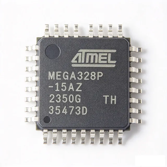
ATMEGA328P-15AZ - 8-bit AVR MCU 32KB Flash TQFP-32 | Microchip
Référence : ATMEGA328P-15AZ ✓ Actif| Qté | Prix unitaire | Total |
|---|---|---|
| 1 | $9.2813 | $9,28 |
| 10 | $6.7031 | $67,03 |
| 100 | $5.9297 | $592,97 |
| 500 | $5.6719 | $2 835,95 |
| 1 000 | $5.4141 | $5 414,10 |
ATMEGA328P-15AZ Présentation
An 8-bit AVR microcontroller is a single-chip processor that integrates a RISC CPU, non-volatile program memory, SRAM, EEPROM, and peripheral functions such as timers, UART, SPI, I2C, and a 10-bit ADC on one die. Within the power-management and embedded-control hierarchy, the AVR family sits in the broader category of microcontroller units (MCUs), competing with PIC, STM8, and 8051 architectures in cost-sensitive embedded systems.
Key features include the advanced RISC architecture with 131 powerful instructions, most executing in a single clock cycle, 32 x 8 general-purpose working registers, and an on-chip 2-cycle hardware multiplier delivering up to 16 MIPS throughput at 16 MHz. The P suffix denotes picoPower technology for ultra-low sleep-mode consumption, critical for battery-powered designs. High-endurance non-volatile memory segments provide 32KB of In-System Self-Programmable Flash with separate boot lock and true read-while-write operation.
Architecturally, the ATmega328P pairs its Harvard-structure CPU with a flexible timer/counter system, USART, SPI, and Two-Wire Interface (I2C), plus a 10-bit successive-approximation ADC that enables direct analog sensor interfacing without external conversion circuitry.
Typical applications include Arduino-compatible boards (the ATmega328P is the classic Arduino Uno/Nano processor), industrial sensor nodes, consumer appliance control, and legacy embedded systems where code and toolchain compatibility matter.
Design consideration: at 5.5V maximum rating, observe total current limits per port and use decoupling capacitors on AVCC and VCC pins; the internal RC oscillator eliminates the need for an external crystal in non-timing-critical designs.
This page synthesizes distributor pricing, drop-in alternatives, pinout data, and practical design notes not consolidated in the manufacturer datasheet.
Alternatives de remplacement direct pour ATMEGA328P-15AZ — même boîtier, compatible broche à broche. Les références à boîtier différent nécessitant une retouche du PCB sont exclues.
Variantes de cette série
Modèles de la même série directement compatibles avec ATMEGA328P-15AZ (même facteur de forme et même empreinte) — différant par Core Architecture, EEPROM, Flash Program Memory, Instructions, Low Power Technology.
Outil de comparaison rapide — sélectionnez des références alternatives pour une comparaison côte à côte :
ATMEGA328P-AU
✓ En stock
$1.74 / unité
Voir la fiche technique →ATMEGA328PB-AU
✓ En stock
$1.12 / unité
Voir la fiche technique →ATMEGA168PA-AU
✓ En stock
$0.98 / unité
Voir la fiche technique →ATMEGA328P-20AU
📋 Alternative de référence (hors catalogue)
LGT8F328P
📋 Alternative de référence (hors catalogue)
ATMEGA328P-15AZ Valeurs maximales et caractéristiques électriques
| Core Architecture | 8-bit AVR RISC |
| Flash Program Memory | 32 KB In-System Self-Programmable |
| SRAM | 2 KB |
| EEPROM | 1 KB |
| Fréquence d'horloge maximale | 20 MHz |
| Supply Voltage Range | 1.8 V to 5.5 V |
| I/O Ports | 32 |
| Throughput | Up to 16 MIPS at 16 MHz |
| Instructions | 131 powerful instructions, most single-cycle |
| Working Registers | 32 x 8 general purpose |
| Multiplier | On-chip 2-cycle hardware multiplier |
| Package Type | 32-TQFP, 10 x 10 mm, 1 mm height, 0.8 mm pitch |
| Type de montage | Surface Mount |
| Low Power Technology | picoPower (P grade) |
| Life Cycle Stage | ACTIVE |
Configuration des broches de ATMEGA328P-15AZ
| Broche 1 | PD3 (PCINT19/OC2B/INT1) — Port D bit 3, pin-change interrupt 19, Timer2 output compare B, external interrupt 1 |
| Broche 2 | PD4 (PCINT20/XCK/T0) — Port D bit 4, pin-change interrupt 20, USART external clock, Timer0 clock input |
| Broche 3 | GND — Ground |
| Broche 4 | VCC — Digital supply voltage |
| Broche 5 | GND — Ground |
| Broche 6 | VCC — Digital supply voltage |
| Broche 7 | PB6 (PCINT6/XTAL1/TOSC1) — Port B bit 6, crystal oscillator pin 1 or timer oscillator input |
| Broche 8 | PB7 (PCINT7/XTAL2/TOSC2) — Port B bit 7, crystal oscillator pin 2 or timer oscillator output |
| Broche 9 | PD5 (PCINT21/OC0B/T1) — Port D bit 5, pin-change interrupt 21, Timer0 output compare B, Timer1 clock input |
| Broche 10 | PD6 (PCINT22/OC0A/AIN0) — Port D bit 6, pin-change interrupt 22, Timer0 output compare A, analog comparator positive input |
| Broche 11 | PD7 (PCINT23/AIN1) — Port D bit 7, pin-change interrupt 23, analog comparator negative input |
| Broche 12 | PB0 (PCINT0/CLKO/ICP1) — Port B bit 0, pin-change interrupt 0, clock output, Timer1 input capture |
| Broche 13 | PB1 (PCINT1/OC1A) — Port B bit 1, pin-change interrupt 1, Timer1 output compare A (PWM) |
| Broche 14 | PB2 (PCINT2/SS/OC1B) — Port B bit 2, pin-change interrupt 2, SPI slave select, Timer1 output compare B (PWM) |
| Broche 15 | PB3 (PCINT3/OC2A/MOSI) — Port B bit 3, pin-change interrupt 3, Timer2 output compare A (PWM), SPI master output |
| Broche 16 | PB4 (PCINT4/MISO) — Port B bit 4, pin-change interrupt 4, SPI master input |
| Broche 17 | PB5 (PCINT5/SCK) — Port B bit 5, pin-change interrupt 5, SPI serial clock |
| Broche 18 | AVCC — ADC supply voltage, connect to VCC through low-pass filter |
| Broche 19 | ADC6 — Analog input channel 6 |
| Broche 20 | AREF — Analog reference voltage for ADC |
| Broche 21 | GND — Ground |
| Broche 22 | ADC7 — Analog input channel 7 |
| Broche 23 | PC0 (ADC8/PCINT8) — Port C bit 0, analog input channel 0, pin-change interrupt 8 |
| Broche 24 | PC1 (ADC9/PCINT9) — Port C bit 1, analog input channel 1, pin-change interrupt 9 |
| Broche 25 | PC2 (ADC10/PCINT10) — Port C bit 2, analog input channel 2, pin-change interrupt 10 |
| Broche 26 | PC3 (ADC11/PCINT11) — Port C bit 3, analog input channel 3, pin-change interrupt 11 |
| Broche 27 | PC4 (ADC12/SDA/PCINT12) — Port C bit 4, analog input channel 4, I2C data line, pin-change interrupt 12 |
| Broche 28 | PC5 (ADC13/SCL/PCINT13) — Port C bit 5, analog input channel 5, I2C clock line, pin-change interrupt 13 |
| Broche 29 | PC6 (RESET/PCINT14) — Reset input (active low), pin-change interrupt 14 |
| Broche 30 | PD0 (PCINT16/RXD) — Port D bit 0, pin-change interrupt 16, USART receive data |
| Broche 31 | PD1 (PCINT17/TXD) — Port D bit 1, pin-change interrupt 17, USART transmit data |
| Broche 32 | PD2 (PCINT18/INT0) — Port D bit 2, pin-change interrupt 18, external interrupt 0 |
Applications typiques
ATMEGA328P-15AZ convient pour 6 applications: Arduino-Compatible Development Boards, Industrial Sensor Nodes, Consumer Appliance Control, Battery-Powered Wearables and Motes, Legacy Embedded System Maintenance, Education and Prototyping.
Arduino-Compatible Development Boards
The ATMEGA328P is the processor of the classic Arduino Uno and Nano platforms, and the ATMEGA328P-15AZ is the TQFP-32 surface-mount variant used on Nano-style boards. Its 32KB Flash accommodates the Arduino bootloader plus user sketches, while the 1.8V to 5.5V supply range and 20 MHz capability match the standard 16 MHz Arduino clocking scheme. The single-cycle RISC core delivers 16 MIPS at 16 MHz, sufficient for typical sketch workloads. Designers of clone or derivative boards benefit from 100% toolchain compatibility with the Arduino IDE and the enormous shield ecosystem, and the picoPower die supports battery-powered derivatives.
Recommandé
Industrial Sensor Nodes
In industrial monitoring nodes, the ATMEGA328P-15AZ combines its integrated 10-bit ADC and I2C/SPI peripherals to read temperature, pressure, and current sensors directly, reducing external component count. The 1.8V to 5.5V supply tolerance tolerates unregulated 5V industrial rails with margin, and picoPower sleep modes extend battery life in wireless nodes that wake on timer or interrupt. The 32KB Flash provides ample room for protocol stacks such as Modbus RTU over the USART, and the 1KB EEPROM stores calibration constants through power cycles. Its wide deployment base and long lifecycle status (ACTIVE) reduce obsolescence risk for multi-year industrial programs.
Recommandé
Consumer Appliance Control
Home appliances such as coffee machines, fans, and small heaters use the ATMEGA328P-15AZ as a low-cost control MCU. The internal 8 MHz RC oscillator eliminates the external crystal and its cost in non-timing-critical appliances, while the 32 general-purpose I/O lines drive seven-segment displays, relays, and touch or button inputs through the TQFP-32 port structure. Hardware PWM channels control motor speed and heater duty cycles with deterministic timing, and the 2-cycle hardware multiplier accelerates PID control loops. The ACTIVE lifecycle and multi-source distributor stock (LCSC, Mouser, DigiKey, Heisener) protect appliance production lines against allocation.
Recommandé
Battery-Powered Wearables and Motes
The picoPower technology that defines the P-grade ATmega328P die makes the -15AZ well suited to coin-cell or Li-ion powered motes and wearable prototypes. Power-down and power-save sleep modes cut consumption to microamp levels (exact figures per the datasheet power-management tables), and the watchdog or asynchronous timer can wake the core periodically for sampling tasks. Running from 1.8V conserves energy with low-voltage sensors, with clock speed derated per the voltage-frequency curve. The 32KB Flash fits lightweight BLE or LoRa framing stacks, and the TQFP-32 10 x 10 mm footprint allows compact two-layer wearable PCBs.
Recommandé
Legacy Embedded System Maintenance
Many deployed industrial and consumer products were designed around the ATmega328P, and the ATMEGA328P-15AZ serves as an active-lifecycle sourcing anchor for that installed base. Because the AVR instruction set, register map, and fuse model have remained stable, replacement parts run legacy firmware without requalification when speed grade and package match. Distributor cross-reference tools (DigiKey, LCSC, Microchip) list parametrically similar substitutes, and the ATMEGA328PB-AU offers an improved but mostly footprint-compatible forward path. The 345-page Atmel datasheet remains the authoritative reference for electrical characteristics during obsolescence-driven redesigns.
Recommandé
Education and Prototyping
Universities and makerspaces standardize on the ATmega328P because the ATMEGA328P-15AZ TQFP part pairs directly with the vast Arduino ecosystem, low-cost ISP programmers, and free toolchains (AVR-GCC, Arduino IDE). Its simple Harvard RISC architecture with 131 mostly single-cycle instructions is an accessible first target for embedded assembly teaching, while the on-chip 10-bit ADC and hardware PWM let students complete analog and motor-control labs without extra boards. The TQFP-32 package also teaches practical surface-mount soldering with a 0.8 mm pitch that is manageable by hand. Community availability of pinout diagrams and reference designs accelerates lab bring-up.
Recommandé
Récapitulatif des produits recommandés
Données de référence d'ingénierie pour ATMEGA328P-15AZ — comparaison, recommandations de conception et informations de conformité.
Guide de sélection
Comparaison avec les alternatives
| Paramètre | Ce produit | ATMEGA328P-AU | ATMEGA328P-20AU | ATMEGA328PB-AU | ATMEGA168PA-AU | LGT8F328P |
|---|---|---|---|---|---|---|
| Package | 32-TQFP (10 x 10 mm, 0.8 mm pitch) | 32-TQFP - same | 32-TQFP - same | 32-TQFP - same | 32-TQFP - same | 32-TQFP - same |
| Brand | Microchip Technology | Microchip Technology | Microchip Technology | Microchip Technology | Microchip Technology | LGT Semiconductor |
| Flash Memory | 32 KB | 32 KB | 32 KB | 32 KB | 16 KB | 32 KB |
| SRAM | 2 KB | 2 KB | 2 KB | 2 KB | 1 KB | 2 KB |
| Pin-Level Drop-In Compatibility | Reference | 100% identical | 100% identical | Two pins differ in function (not official drop-in) | Pinout identical, memory reduced | Pin-compatible clone per community verification |
| Peripherals / Timers | 3 timers, 1 USART, SPI, I2C, 10-bit ADC | Same as this product | Same as this product | More timers, USARTs, I2C/SPI interfaces | Fewer peripherals than 328P family | Adds 16-bit-capable PWM |
Principaux différenciateurs
- Guaranteed 100% pin-level compatibility with legacy ATmega328P designs (vs ATMEGA328PB-AU)
- Full Arduino ecosystem and official vendor support (vs LGT8F328P)
- Double the program memory versus smaller pin-compatible siblings (vs ATMEGA168PA-AU)
- picoPower technology for battery designs (vs ATMEGA328P-20AU)
Notes de conception
Connect AVCC (pin 18) to VCC through a low-pass filter (for example a 10 uH inductor or ferrite bead plus 100 nF capacitor) to keep ADC noise low, per the ATmega328P datasheet ADC section recommendations. Place 100 nF ceramic decoupling capacitors directly at both VCC pins (4 and 6) plus the GND pins (3 and 5). If operating near 20 MHz at 5V, verify supply ripple stays within the 1.8V to 5.5V absolute range under worst-case load to avoid brown-out resets; enable the internal brown-out detector (BOD) fuse for robust operation.
In the 32-TQFP (0.8 mm pitch, 10 x 10 mm) footprint, route the crystal traces for PB6/PB7 (XTAL1/XTAL2) as short as possible with guard ground, and keep the AREF (pin 20) trace away from fast digital signals. If you use the internal RC oscillator, PB6/PB7 become general-purpose I/O and the crystal can be omitted, simplifying two-layer layouts. Provide thermal reliefs for hand assembly, and expose pin 1 marker alignment to avoid 90-degree rotation errors, which are a common prototype soldering fault on TQFP-32.
Maximum clock speed depends on supply voltage: the 20 MHz rating applies only at the higher end of the 1.8V to 5.5V range, so derate frequency at low voltage per the datasheet frequency-versus-voltage curve. When migrating to the ATMEGA328PB-AU, note it is officially not a 100% drop-in; two pins differ in function per Microchip documentation, so verify PCB connectivity first. When burning fuses, never set the clock source fuses incorrectly with no external clock connected, as this can lock the chip out of ISP programming (recovery requires a high-voltage parallel programmer).
On battery or long-wire powered nodes, add a 100 nF capacitor close to the RESET pin (29) and a 10 kOhm pull-up to prevent spurious resets from cable transients. The RESET pin doubles as PCINT14 and is driven low during programming, so do not overload it with other functions. Keep I2C SDA/SCL (PC4/PC5) bus lengths short with proper pull-up sizing (typically 4.7 kOhm at 5V, 100 kHz) to maintain rise-time margins on the open-drain bus.
Informations de conformité
Compliance status not explicitly stated in the provided verified web data; verify on the official Microchip product page or distributor compliance sheets. Modern Microchip AVR parts are generally RoHS compliant, but this was not confirmed in the supplied sources.







