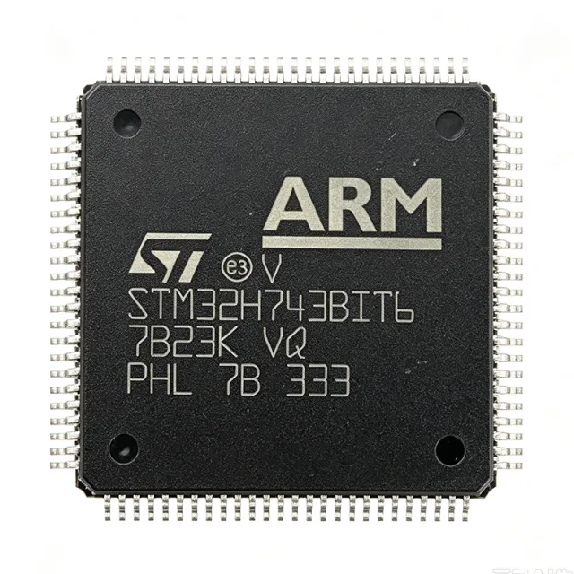
STM32H743BIT6 - 480MHz Cortex-M7 MCU, 2MB Flash | STMicroelectronics
Référence : STM32H743BIT6 ✓ Actif| Qté | Prix unitaire | Total |
|---|---|---|
| 1 | $18.5 | $18,50 |
| 10 | $16.2 | $162,00 |
| 100 | $13.85 | $1 385,00 |
| 500 | $11.4 | $5 700,00 |
| 1 000 | $9.85 | $9 850,00 |
STM32H743BIT6 Présentation
What is a microcontroller (MCU)? A microcontroller is a compact integrated circuit that combines a processor core, program memory (Flash), working memory (RAM), and programmable peripherals on a single die. Within the wider taxonomy, the STM32H743BIT6 sits in the high-performance MCU category: Arm Cortex-M7 -> Cortex-M family -> 32-bit MCU -> microcontroller -> embedded processor. The H7 line targets demanding applications that exceed Cortex-M4 throughput but do not require a full applications processor.
Key specifications include 480 MHz core speed with 1284 CoreMark performance, 2 MB dual-bank Flash supporting read-while-write, and 1 MB SRAM configurable as 192 KB DTCM + 64 KB ITCM + 1 MB AXI-SRAM. Connectivity options include 10/100 Ethernet, USB 2.0 OTG HS/FS, CAN FD, SDMMC, three SPI plus one half-duplex SPI, four I2C, four USART/UART/LPUART, and two SAI. Analog peripherals include three 16-bit ADCs, two DAC channels, two comparators, and an SMBus-PMBus controller. Hardware crypto acceleration, TRNG, secure boot, and one-time-programmable (OTP) fuses round out the security perimeter.
Architecturally, the STM32H743BIT6 uses a 7-stage pipeline with branch prediction, an L1 instruction cache, an MPU, and a Chrom-ART 2D graphics accelerator. The device supports separate core voltage domains via an integrated SMPS step-down converter and an LDO, with VDD range of 1.62 V to 3.6 V. This dual-rail power architecture allows dynamic voltage scaling for power-constrained designs without external PMICs.
Typical uses include industrial motor control (field-oriented control and PMSM drives), factory automation controllers, audio sub-systems with MPU-decoded codecs, USB peripherals with HID or mass-storage stacks, secure gateways with TLS offload via hardware crypto, building automation touchpanels, and IoT edge nodes requiring on-device ML inference via CMSIS-NN libraries.
When designing with this MCU, ensure the SMPS inductor is sized per the datasheet reference design and that VDD/VDDA/VBAT pins each have local decoupling. RoHS/REACH compliance and industrial-grade temperature range (-40 C to +85 C, +105 C Tj) make the part suitable for ruggedized applications. This page synthesizes distributor pricing, drop-in pin-compatible alternatives, and design notes that augment the manufacturer datasheet.
Alternatives de remplacement direct pour STM32H743BIT6 — même boîtier, compatible broche à broche. Les références à boîtier différent nécessitant une retouche du PCB sont exclues.
Variantes de cette série
Modèles de la même série directement compatibles avec STM32H743BIT6 (même facteur de forme et même empreinte) — différant par Flash Memory, Package.
Outil de comparaison rapide — sélectionnez des références alternatives pour une comparaison côte à côte :
STM32H753BIT6
✅ Remplacement direct📋 Alternative de référence (hors catalogue)
STM32H750IBT6
✅ Remplacement direct✓ En stock
$8.85 / unité
Voir la fiche technique →STM32H743BIT6 Valeurs maximales et caractéristiques électriques
| Core Architecture | Arm Cortex-M7 with FPU (DP-FPU) |
| Maximum CPU Clock | 480 MHz |
| Flash Memory | 2 MB dual-bank |
| SRAM | 1 MB total (192 KB DTCM + 64 KB ITCM + 1 MB AXI-SRAM) |
| CoreMark Score | 1284 (typical) |
| Supply Voltage VDD | 1.62 V to 3.6 V |
| Operating Temperature (junction) | -40 C to +105 C (industrial) |
| Boîtier | 208-LQFP, 28x28 mm |
| Type de montage | Surface Mount |
| GPIO Count | Up to 168 (depending on configuration) |
| Communication Interfaces | Ethernet MAC, USB OTG HS/FS, CAN FD x2, SDMMC, 4xSPI, 4xI2C, 4xUSART/UART/LPUART, 2xSAI |
| Analog Peripherals | 3x16-bit ADC, 2x12-bit DAC, 2xcomparator |
| Hardware Crypto | AES, Hash, TRNG, PKA, secure firmware install |
| Graphics | Chrom-ART 2D accelerator, JPEG codec |
| Timers | Advanced-control timers, HRTIM, low-power timers |
| Statut RoHS | Compliant |
| Niveau de sensibilité à l'humidité (MSL) | MSL3 (168 h) |
Guide de configuration des broches du STM32H743BIT6 208-lqfp, 28x28 mm
Configuration des broches du STM32H743BIT6 (boîtier 208-lqfp, 28x28 mm). Ce circuit intégré numérique comprend des GPIO, des interfaces de communication (UART, SPI, I2C) et des broches d'alimentation. Consultez la fiche technique du fabricant pour les fonctions alternatives des broches et les options de configuration. Indispensable pour la conception de systèmes embarqués et la conception de circuits imprimés.

Aucune donnée de brochage détaillée disponible pour STM32H743BIT6.
Consultez la fiche technique pour la configuration complète des broches.
Applications typiques
STM32H743BIT6 convient pour 6 applications: Industrial PMSM Motor Control and Field-Oriented Control Drives, Industrial Human-Machine Interface Panels with Touch and Graphics, High-End USB Audio Interfaces with 24-bit / 192 kHz Streaming, Secure IoT Gateways with Ethernet and TLS Offload, Aerospace Telemetry and Avionics Subsystems, High-Speed Vision Processing and Industrial Camera Front-Ends.
Industrial PMSM Motor Control and Field-Oriented Control Drives
The STM32H743BIT6 is a leading choice for 3-phase PMSM and BLDC motor drives in industrial servo, robotics, and CNC machinery. Its 480 MHz Cortex-M7 throughput runs space-vector PWM and field-oriented control loops with under 10 microsecond cycle times; the dedicated HRTIM timer achieves 184 ps resolution for transformer-less totem-pole PFC. Three 16-bit ADCs at 3.6 MSPS, paired with HRTIM triggering, enable single-shunt or three-shunt current reconstruction with low phase delay. The 1 MB SRAM accommodates long buffer traces for predictive maintenance analytics without off-chip memory. The part is complemented by ST's MC SDK reference firmware, allowing rapid drop-in evaluation on STEVAL-SPIN3201 and similar boards.
Recommandé
Industrial Human-Machine Interface Panels with Touch and Graphics
Factories and process-control rooms increasingly require HMI panels that render complex graphics, animations, and touchscreen responses locally. The STM32H743BIT6 excels here with its Chrom-ART 2D acceleration engine and hardware JPEG codec, offloading frame composition from the CPU. Driving an 800x480 WXGA LTDC display is straightforward via the TFT controller in continuous mode. Dual-bank Flash supports safe field updates, while the 2 MB code space hosts full GUI frameworks such as TouchGFX or LVGL without external QSPI. Hardware TRNG and Secure Firmware Install protect against IP cloning, vital in regulated factory automation contexts.
Recommandé
High-End USB Audio Interfaces with 24-bit / 192 kHz Streaming
USB-based audio interfaces, mixers, and DAW peripherals benefit from the STM32H743BIT6's 480 MHz processing headroom for 32-bit double-precision DSP, SAI interfaces, and the high-speed USB OTG controller with built-in PHY. Audio-class driver stacks (UAC2) run natively, and ST's USB-Device library supports asynchronous feedback modes required for bit-perfect playback. The SAI peripheral streams two simultaneous audio streams in TDM with eight channels each, accommodating multichannel studio gear. Software-implemented effects typically leave 60% CPU for further expansion, allowing boutique vendors to add reverb or mastering chains without external DSP.
Recommandé
Secure IoT Gateways with Ethernet and TLS Offload
IoT edge gateways require simultaneous Ethernet, TLS, and protocol translation. The STM32H743BIT6 combines an integrated 10/100 Ethernet MAC with hardware AES-256 and SHA accelerators that offload mbedTLS or WolfSSL sessions, sustaining hundreds of TLS handshakes per second while leaving Cortex-M7 cycles for application logic. TRNG and PKA accelerators deliver secure key generation and ECDSA verification. With 2 MB Flash and 1 MB SRAM, the gateway can host a full Linux-like IP stack (LwIP or OpenThread) plus provisioning firmware, eliminating external secure-element ICs in many designs.
Recommandé
Aerospace Telemetry and Avionics Subsystems
Avionics subsystems such as flight controllers, sensor fusion units, and navigation processors value the STM32H743BIT6's -40 to +105 C operating range, AEC-Q100 qualified process, and double-precision FPU for navigation-equation updates. With external barometric and IMU companions, the part computes 1 kHz quaternion updates while running CMSIS-DSP libraries for sensor fusion. The 168 GPIO handles parallel LVDS data taps from optical encoders. Hardware crypto acceleration supports secure boot chains demanded in DO-178-qualified flight stacks, while dual-bank Flash enables firmware rollback in fault scenarios.
Recommandé
High-Speed Vision Processing and Industrial Camera Front-Ends
The STM32H743BIT6 anchors smart-camera designs with parallel DCMI interface supporting up to 12-bit wide image sensor capture at 80 MHz pixel clock. Chrom-ART accelerates overlay rendering, while the JPEG codec compresses QVGA streams under 2 ms. Designs leverage USB 2.0 HS for video-class streaming or Ethernet for IP-camera back-haul. The Cortex-M7 DSP SIMD is ideal for Kmeans clustering, histogram equalization, and on-device lightweight CNN inference via CMSIS-NN. This combination suits machine vision pre-processing tasks in food sorting, PCB inspection, and traffic-monitor cameras.
Recommandé
Récapitulatif des produits recommandés
Données de référence d'ingénierie pour STM32H743BIT6 — comparaison, recommandations de conception et informations de conformité.
Guide de sélection
Comparaison avec les alternatives
| Paramètre | Ce produit | STM32H753BIT6 | STM32H750IBT6 | STM32H743IIT6 | STM32H742VIT6 |
|---|---|---|---|---|---|
| Brand | STMicroelectronics | STMicroelectronics | STMicroelectronics | STMicroelectronics | STMicroelectronics |
| Package | 208-LQFP (28x28 mm) | 208-LQFP - same | 208-LQFP - same | 176-LQFP (24x24) - smaller | 100-LQFP (14x14) - smaller |
| Maximum CPU Clock | 480 MHz | 480 MHz | 480 MHz | 480 MHz | 480 MHz |
| Flash | 2 MB | 2 MB | 128 KB (+ external SPI Flash required) | 2 MB | 2 MB |
| SRAM | 1 MB | 1 MB | 1 MB | 1 MB | 1 MB |
| Hardware Crypto | TRNG only | AES, SHA, PKA, TRNG (full) | TRNG | TRNG only | TRNG only |
| GPIO Count (max) | 168 | 168 | 168 | 140 | 82 |
| USB OTG | HS + FS | HS + FS | FS only | HS + FS | HS + FS |
Principaux différenciateurs
- Highest Cortex-M7 throughput in LQFP footprint with full crypto-ready sibling on same package (vs STM32H753BIT6 vs STM32H743BIT6)
- Smaller-footprint pin-compatible siblings reduce PCB area up to 60% (vs STM32H742VIT6 vs STM32H743BIT6)
- Optional 128 KB internal Flash + external QSPI NOR reduces -54% of code footprint (vs STM32H750IBT6 vs STM32H743BIT6)
Notes de conception
The STM32H743BIT6 integrates a SMPS step-down converter that supplies VCORE when the regulator is in SMPS mode. Place the 4.7 uH inductor (L1) close to VDD_LVL pins, as recommended in STM32H7 reference designs. Switching frequency is software-configurable (default 4 MHz). Ensure the SMPS output capacitor is at least 4.7 uF low-ESR ceramic to avoid ripple on VCORE that could destabilize clocks. Estimated: at full 480 MHz operation, the SMPS delivers roughly 60-100 mA.
Place 100 nF decoupling capacitors on every VDD/VDDA/VBAT pin, plus 4.7 uF bulk on each power rail within 5 mm. The 208-LQFP's exposed pad is not present on this package, so the thermal dissipation is via the 1.5 oz copper pours under the die. A continuous ground plane beneath the package cuts radiated emissions. Keep HS-USB traces 90 ohm differential and length-matched to within 150 mil.
At full 480 MHz with all peripherals active, the STM32H743BIT6 dissipates around 350 mW. Junction-to-ambient thermal resistance of the 208-LQFP is roughly 30 C/W, yielding a 10 C rise above ambient in still air. For applications pushing 100% duty cycle such as field-oriented motor control, ensure adequate PCB copper area (>= 50x50 mm). Estimated: junction temperature reaches about 70 C at +60 C ambient - well within the 105 C Tj rating.
SDRAM interfaces on the STM32H743BIT6 require impedance-matched traces to 50 ohm; address/clock lines should be routed length-matched with a max delta of 1 cm. Use IBIS simulation from ST to validate. Failure to length-match produces sub-bit errors on the FMC that are notoriously hard to debug.
Engineering pitfall: leaving PWR_LP_ON mode at 480 MHz may cause hang-ups on wake-up - configure RCC after wake before any peripheral touches. Another: Boot-pin (BOOT0) must be pulled correctly at reset; it is sampled on NRST rising edge. Avoid re-routing boot pins through glue logic without debouncing. Finally, do not enable both SMPS and LDO simultaneously in bypass mode without consulting the errata (resolved in revision Y).
Informations de conformité
RoHS and REACH compliant per ST product page. AEC-Q100 qualified process for industrial / automotive grade. Halogen-free per vendor datasheet. Conflict-minerals statement available on ST corporate compliance portal.







