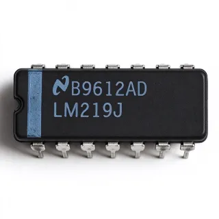
CD4024BFX - 7-Bit Binary Counter, 14-CDIP | Harris Corporation
Référence : CD4024BFX ✗ Fin de vieCD4024BFX Présentation
A binary counter is a sequential digital-logic component that advances through a defined sequence of states when it receives an active clock transition. The CD4024BFX belongs to the CD4000 CMOS logic family, whose hierarchy is binary counter → counter IC → logic IC → digital semiconductor. Unlike a free-running oscillator, it advances only in response to its clock input, allowing a system to divide an incoming frequency into a lower binary-coded rate.
The CD4024BFX provides one 7-bit counting element, negative-edge triggering, and a ripple-carry architecture. These features make it suitable for frequency division, modulo operation, event counting, timing intervals, and digital state sequencing. Its 14-CDIP construction also supports insertion into legacy sockets and hand-wired or stitched PCB assemblies. The manufacturer datasheet should be consulted for detailed electrical limits, setup timing, reset behavior, and environmental ratings before production use.
Because this is a ripple-carry counter, propagation delay accumulates through the internal stages. The longest delay occurs between the first clocked stage and the final carry output. This characteristic makes the device most appropriate where one carry output is needed and moderately cascaded timing is acceptable, rather than for applications demanding simultaneous high-speed outputs from multiple counter sections.
Typical uses include binary frequency division in industrial control equipment, pulse counting in test and measurement systems, programmable timing chains in legacy computing equipment, and sequential address or state generation. The negative-edge clock trigger allows the counter to change state on the falling transition of the clock waveform, which can simplify edge-sensitive interfacing with surrounding CMOS logic.
PCB integration requires the 14-CDIP footprint and attention to signal-integrity practices, including short clock and reset traces, adequate bypass capacitance, and protection from unused inputs. Designers should also account for the cumulative ripple delay when cascading multiple counters or deriving timing from the terminal carry output.
This product record combines package identification, counter characteristics, drop-in replacement considerations, comparison data, and practical implementation guidance. It is intended to support engineering selection and sourcing decisions for legacy Harris CD4024BFX assemblies rather than substituting a modern surface-mount design without appropriate timing, environmental, and lifecycle review.
Alternatives de remplacement direct pour CD4024BFX — même boîtier, compatible broche à broche. Les références à boîtier différent nécessitant une retouche du PCB sont exclues.
Variantes de cette série
Modèles de la même série directement compatibles avec CD4024BFX (même facteur de forme et même empreinte) — différant par Counter Type, Logic Family, Package Type.
CD4024BE
✅ Remplacement directContactez-nous pour le prix
Voir la fiche technique →CD4024BP
✅ Remplacement direct📋 Alternative de référence (hors catalogue)
HCF4024BEY
✅ Remplacement direct📋 Alternative de référence (hors catalogue)
JM38510/05655BCA
✅ Remplacement direct📋 Alternative de référence (hors catalogue)
CD4024BHSR
✅ Remplacement directContactez-nous pour le prix
Voir la fiche technique →CD4024BFX Valeurs maximales et caractéristiques électriques
| Counter Type | Binary counter |
| Number of Counting Elements | 1 element |
| Counter Resolution | 7 bit |
| Clock Edge | Negative edge |
| Logic Family | CMOS CD4000 series |
| Architecture | Ripple-carry binary counter |
| Package Type | 14-CDIP |
| Number of Terminals | 14 terminals |
| Style de montage | Through-hole |
| Package Shape | Rectangular DIP |
| Temperature Grade | Military |
Guide de configuration des broches du CD4024BFX rectangular dip
Configuration des broches du CD4024BFX (boîtier rectangular dip). Ce circuit intégré numérique comprend des GPIO, des interfaces de communication (UART, SPI, I2C) et des broches d'alimentation. Consultez la fiche technique du fabricant pour les fonctions alternatives des broches et les options de configuration. Indispensable pour la conception de systèmes embarqués et la conception de circuits imprimés.

Aucune donnée de brochage détaillée disponible pour CD4024BFX.
Consultez la fiche technique pour la configuration complète des broches.
Applications typiques
CD4024BFX convient pour 6 applications: Industrial Frequency Divider, Pulse and Event Counter, Legacy Timing Chain, Digital State Sequencer, Test and Measurement Equipment, Aerospace and Defense Retrofit.
Industrial Frequency Divider
The CD4024BFX suits legacy industrial timing circuits that divide a clock into a lower binary-coded frequency. Its 7-bit counter provides 128 states, while the negative-edge trigger establishes a deterministic state transition. The 14-CDIP package also allows reuse of an existing through-hole controller board. The principal design consideration is ripple delay: timing from the first output to the terminal carry accumulates across the internal stages. Confirm maximum clock frequency and output transition limits in the manufacturer datasheet, and route the clock away from sensitive analog sections.
Recommandé
Pulse and Event Counter
CD4024BFX can count incoming pulses in legacy instrumentation when a system requires binary event totals rather than a display-oriented counter IC. The single 7-bit counting element produces a modulo-128 count, and the negative-edge clock trigger can be aligned with a pulse source. Engineers should verify the allowable input pulse width and setup time before using it directly with slow or noisy mechanical contacts. Debouncing, conditioning, and clock-schmitt design remain external concerns because the CD4024BFX does not eliminate input-contact bounce.
Recommandé
Legacy Timing Chain
The CD4024BFX is appropriate for programmable timing and delayed-event circuits built around older CMOS control logic. Its 7-bit count permits binary tap selection, while the 14-CDIP package simplifies replacement in through-hole equipment. Designers should not assume that the terminal carry arrives simultaneously with lower-order outputs because the ripple architecture introduces cumulative propagation delay. Use the manufacturer timing characteristics to establish setup and hold margins, and avoid using a near-terminal carry as an edge-sensitive clock without sufficient margin.
Recommandé
Digital State Sequencer
CD4024BFX can serve as the modulo-128 element in a legacy digital sequencer that advances through binary states after each active clock edge. The counter outputs provide a compact state vector for combinational decoding, while the negative-edge transition gives designers a defined update point. Because only one counting element is present, cascaded devices are required for wider state spaces. The design must include analysis of cumulative ripple delay and must use the datasheet pin-description table to avoid assigning reserved or duplicated outputs incorrectly.
Recommandé
Test and Measurement Equipment
The CD4024BFX can support frequency division and event-counting functions in legacy test and measurement equipment that uses through-hole CMOS logic. A 7-bit counter divides a periodic input into a lower-rate binary sequence, which may feed display, trigger, or control logic. Keep the clock path short and isolate the counter from high-impedance analog nodes to reduce coupling. The military-grade target is relevant when the original equipment specifies a qualified counter for extended environmental operation, while lower-grade alternatives require a separate operating-temperature review.
Recommandé
Aerospace and Defense Retrofit
CD4024BFX is suited to maintaining legacy aerospace, defense, or other high-reliability through-hole systems whose original schematics call for a military-grade CD4000-series counter. The 14-CDIP format allows socketed implementation, and the 7-bit counter architecture preserves legacy binary-count behavior. Substitution should be treated as a controlled qualification exercise: compare operating-temperature grade, timing, radiation or screening expectations, and provenance requirements. Because the binary-counter function matches, the decisive engineering issue is qualification rather than state resolution.
Recommandé
Récapitulatif des produits recommandés
Données de référence d'ingénierie pour CD4024BFX — comparaison, recommandations de conception et informations de conformité.
Guide de sélection
Comparaison avec les alternatives
| Paramètre | Ce produit | CD4024BE | CD4024BP | HCF4024BEY | JM38510/05655BCA | CD4024B |
|---|---|---|---|---|---|---|
| Package | 14-CDIP | 14-CDIP | 14-CDIP | 14-DIP | 14-DIP | 14-CDIP |
| Brand | Harris Corporation | Texas Instruments | Texas Instruments | STMicroelectronics | Microchip Technology | Texas Instruments |
| Counter Resolution | 7 bit | 7 bit | 7 bit | 7 bit | 7 bit | 7 bit |
| Mounting Type | Through-hole | Through-hole | Through-hole | Through-hole | Through-hole | Through-hole |
Principaux différenciateurs
- Military-grade CD4024B qualification (vs CD4024BE)
- Wide stated operating range in an equivalent DIP device (vs HCF4024BEY)
- Exact binary-counter architecture preserved (vs JM38510/05655BCA)
- Socket-compatible 14-terminal ceramic DIP construction (vs CD4024BP)
Notes de conception
Do not treat the CD4024BFX as a synchronous counter. The lower-order outputs change before the terminal carry because propagation delay accumulates through the ripple chain. Use the manufacturer timing characteristics to establish the interval between the first output transition and the final carry. If another device samples the carry on the same clock edge, add sufficient delay or redesign the timing chain so the sampling edge occurs after the worst-case ripple delay.
Preserve a conventional 14-pin DIP land pattern with 300 mil row spacing and 100 mil pitch. Keep the clock route short, connect the supply pins to a low-impedance plane, and place the required bypass capacitor close to the device. When upgrading a legacy board, inspect socket tension, pin oxidation, solder bridging, and lead-frame alignment; these mechanical conditions can matter more than the nominal logic function in a long-lived assembly.
Do not switch the CD4024BFX clock directly from a noisy mechanical contact or a slow-changing analog node. Use a conditioned clock with adequate rise and fall times and ensure that reset inputs cannot float. Review every input for voltage levels compatible with the CD4000-series supply range. For cascaded counters, route the terminal carry to the next clock with enough trace isolation to prevent simultaneous switching noise from disturbing the source device.
CD4024BFX is a low-power logic counter rather than a power-conversion component, but environmental qualification still governs its use. The target is identified as military-grade, while the suitable operating-temperature range is not stated in the available product listing. Verify the datasheet limits and system ambient temperature before installation. If a substitute offers a wider stated range, confirm that its input thresholds, timing, and supply limits remain compatible with the original circuit.
Informations de conformité
The available product information identifies the CD4024BFX as a military-grade Harris Corporation CMOS counter but does not state RoHS, REACH, lead-free, halogen-free, or conflict-minerals status. AEC-Q100 is not applicable because the part is not identified as an automotive-qualified device.