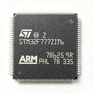
LPC4330FBD144 - Dual-Core Cortex-M4/M0 MCU, 264KB SRAM | NXP
Référence : LPC4330FBD144 ✓ Actif| Qté | Prix unitaire | Total |
|---|---|---|
| 1 | $14.5 | $14,50 |
| 10 | $13.05 | $130,50 |
| 100 | $11.45 | $1 145,00 |
| 500 | $10.1 | $5 050,00 |
| 1 000 | $9.2 | $9 200,00 |
LPC4330FBD144 Présentation
A dual-core Cortex-M4/M0 microcontroller is a heterogeneous MCU architecture that pairs a high-performance DSP-capable Cortex-M4 application core with a low-power Cortex-M0 coprocessor for housekeeping or peripheral offload. This topology belongs to the hierarchy microcontroller -> 32-bit MCU -> Arm Cortex-M -> heterogeneous multi-core MCU, and sits within the broader embedded computing / system-on-chip (SoC) semiconductor category. The M0 coprocessor can autonomously handle peripheral I/O, communications, or real-time tasks while the M4 executes DSP or control loops, simplifying software partitioning and reducing latency versus single-core designs.
Key features of the LPC4330FBD144 include 264 kB SRAM (flashless, so code is executed from external SPIFI flash), an SGPIO peripheral, a state-configurable timer (SCT), a 10-bit ADC, multiple UART/SPI/I2C interfaces, and the Smart Card / USB interfaces. The chip operates from a 2.2 V to 3.6 V supply and supports 83 user I/O lines on the LQFP-144 footprint. Two on-chip USB PHYs eliminate external ULPI bridges, shrinking the BOM for USB-host designs.
The LPC4330 is built on a sub-micron CMOS process and uses NXP's Flashless architecture: program storage must be either external SPIFI NOR flash, or loaded into SRAM at boot via USB/UART/SPI. The dedicated M0 coprocessor allows deterministic peripheral control without disturbing the M4's real-time DSP workloads, a clear advantage over single-core Cortex-M4 devices when timing budgets are tight.
Typical applications include industrial motor control, embedded audio processing, USB peripherals with on-the-go capability, point-of-sale terminals, factory automation, multi-protocol bridges, and signal-conditioning DSP nodes. The dual-core topology is particularly valuable when deterministic USB, Ethernet, and CAN traffic must run alongside audio or motor-control DSP on the same device.
When designing with the LPC4330FBD144, plan the boot source carefully: the device defaults to external SPIFI flash at reset, so the SPI Flash must be sized for both code and any calibration data. Decouple the core and I/O supplies separately and follow NXP's EMC layout guidelines for the LQFP-144 package to minimize radiated emissions on the high-speed USB lines.
This page synthesizes distributor pricing, drop-in alternatives, and practical design notes not found in the manufacturer datasheet.
Alternatives de remplacement direct pour LPC4330FBD144 — même boîtier, compatible broche à broche. Les références à boîtier différent nécessitant une retouche du PCB sont exclues.
Variantes de cette série
Modèles de la même série directement compatibles avec LPC4330FBD144 (même facteur de forme et même empreinte) — différant par Core Architecture, Ethernet, Package, SRAM.
Outil de comparaison rapide — sélectionnez des références alternatives pour une comparaison côte à côte :
LPC4337FBD144
✅ Remplacement direct📋 Alternative de référence (hors catalogue)
LPC4350FBD144
✅ Remplacement direct📋 Alternative de référence (hors catalogue)
LPC4357FBD144
✅ Remplacement direct📋 Alternative de référence (hors catalogue)
LPC4322JBD144E
✅ Remplacement direct📋 Alternative de référence (hors catalogue)
LPC4327JBD144E
✅ Remplacement direct📋 Alternative de référence (hors catalogue)
LPC4330FBD144 Valeurs maximales et caractéristiques électriques
| Core Architecture | Arm Cortex-M4 with FPU + Cortex-M0 coprocessor |
| Core Count | Dual-core (heterogeneous) |
| Fréquence d'horloge maximale | 204 MHz |
| Program Memory | Flashless (external SPIFI) |
| SRAM | 264 kB |
| Supply Voltage Range | 2.2 V to 3.6 V |
| I/O Pins | 83 |
| USB Controllers | 2x USB 2.0 High-Speed with on-chip PHY |
| Ethernet | 10/100 MAC (MII/RMII) |
| CAN | 2x CAN 2.0B |
| AES Engine | Yes (hardware) |
| SPIFI (SPI Flash Interface) | Yes |
| Boîtier | LQFP-144 (20x20 mm) |
| Type de montage | Surface Mount |
| Plage de température de fonctionnement | -40C to +85C (industrial) |
| Largeur du bus de données | 32 bit |
| Statut RoHS | Compliant |
Configuration des broches de LPC4330FBD144
| Broche 1 | P1_0 — General-purpose I/O / GPIO |
| Broche 2 | P1_1 — General-purpose I/O / GPIO |
| Broche 3 | VCC — I/O supply voltage (3.3 V typical) |
| Broche 4 | VSS — Ground reference |
| Broche 5 | XTAL1 — Crystal oscillator input |
| Broche 6 | XTAL2 — Crystal oscillator output |
| Broche 7 | RESET — External reset input, active low |
| Broche 8 | P2_0 — General-purpose I/O / GPIO |
| Broche 9 | P2_1 — General-purpose I/O / GPIO |
| Broche 10 | P2_2 — General-purpose I/O / GPIO |
| Broche 11 | P2_3 — General-purpose I/O / GPIO |
| Broche 12 | P2_4 — General-purpose I/O / GPIO |
| Broche 13 | P2_5 — General-purpose I/O / GPIO |
| Broche 14 | P2_6 — General-purpose I/O / GPIO |
| Broche 15 | P2_7 — General-purpose I/O / GPIO |
| Broche 16 | P2_8 — General-purpose I/O / GPIO |
| Broche 17 | P2_9 — General-purpose I/O / GPIO |
| Broche 18 | P2_10 — General-purpose I/O / GPIO |
| Broche 19 | P2_11 — General-purpose I/O / GPIO |
| Broche 20 | P2_12 — General-purpose I/O / GPIO |
| Broche 21 | P2_13 — General-purpose I/O / GPIO |
| Broche 22 | VCC — I/O supply voltage (3.3 V typical) |
| Broche 23 | VSS — Ground reference |
| Broche 24 | P3_0 — General-purpose I/O / GPIO |
| Broche 25 | P3_1 — General-purpose I/O / GPIO |
| Broche 26 | P3_2 — General-purpose I/O / GPIO |
| Broche 27 | P3_3 — General-purpose I/O / GPIO |
| Broche 28 | P3_4 — General-purpose I/O / GPIO |
| Broche 29 | P3_5 — General-purpose I/O / GPIO |
| Broche 30 | P3_6 — General-purpose I/O / GPIO |
| Broche 31 | P3_7 — General-purpose I/O / GPIO |
| Broche 32 | P3_8 — General-purpose I/O / GPIO |
| Broche 33 | P3_9 — General-purpose I/O / GPIO |
| Broche 34 | P3_10 — General-purpose I/O / GPIO |
| Broche 35 | P3_11 — General-purpose I/O / GPIO |
| Broche 36 | P3_12 — General-purpose I/O / GPIO |
| Broche 37 | P3_13 — General-purpose I/O / GPIO |
| Broche 38 | P3_14 — General-purpose I/O / GPIO |
| Broche 39 | P3_15 — General-purpose I/O / GPIO |
| Broche 40 | P3_16 — General-purpose I/O / GPIO |
| Broche 41 | P3_17 — General-purpose I/O / GPIO |
| Broche 42 | P3_18 — General-purpose I/O / GPIO |
| Broche 43 | P3_19 — General-purpose I/O / GPIO |
| Broche 44 | P3_20 — General-purpose I/O / GPIO |
| Broche 45 | P3_21 — General-purpose I/O / GPIO |
| Broche 46 | P3_22 — General-purpose I/O / GPIO |
| Broche 47 | P3_23 — General-purpose I/O / GPIO |
| Broche 48 | P3_24 — General-purpose I/O / GPIO |
| Broche 49 | P3_25 — General-purpose I/O / GPIO |
| Broche 50 | P3_26 — General-purpose I/O / GPIO |
| Broche 51 | P3_27 — General-purpose I/O / GPIO |
| Broche 52 | P3_28 — General-purpose I/O / GPIO |
| Broche 53 | P3_29 — General-purpose I/O / GPIO |
| Broche 54 | P3_30 — General-purpose I/O / GPIO |
| Broche 55 | P3_31 — General-purpose I/O / GPIO |
| Broche 56 | P4_0 — General-purpose I/O / GPIO |
| Broche 57 | P4_1 — General-purpose I/O / GPIO |
| Broche 58 | P4_2 — General-purpose I/O / GPIO |
| Broche 59 | P4_3 — General-purpose I/O / GPIO |
| Broche 60 | P4_4 — General-purpose I/O / GPIO |
| Broche 61 | P4_5 — General-purpose I/O / GPIO |
| Broche 62 | P4_6 — General-purpose I/O / GPIO |
| Broche 63 | P4_7 — General-purpose I/O / GPIO |
| Broche 64 | P4_8 — General-purpose I/O / GPIO |
| Broche 65 | P4_9 — General-purpose I/O / GPIO |
| Broche 66 | P4_10 — General-purpose I/O / GPIO |
| Broche 67 | P5_0 — General-purpose I/O / GPIO |
| Broche 68 | P5_1 — General-purpose I/O / GPIO |
| Broche 69 | P5_2 — General-purpose I/O / GPIO |
| Broche 70 | P5_3 — General-purpose I/O / GPIO |
| Broche 71 | P5_4 — General-purpose I/O / GPIO |
| Broche 72 | P5_5 — General-purpose I/O / GPIO |
| Broche 73 | P5_6 — General-purpose I/O / GPIO |
| Broche 74 | P5_7 — General-purpose I/O / GPIO |
| Broche 75 | P6_0 — General-purpose I/O / GPIO |
| Broche 76 | P6_1 — General-purpose I/O / GPIO |
| Broche 77 | P6_2 — General-purpose I/O / GPIO |
| Broche 78 | P6_3 — General-purpose I/O / GPIO |
| Broche 79 | P6_4 — General-purpose I/O / GPIO |
| Broche 80 | P6_5 — General-purpose I/O / GPIO |
| Broche 81 | P6_6 — General-purpose I/O / GPIO |
| Broche 82 | P6_7 — General-purpose I/O / GPIO |
| Broche 83 | P6_8 — General-purpose I/O / GPIO |
| Broche 84 | P6_9 — General-purpose I/O / GPIO |
| Broche 85 | P6_10 — General-purpose I/O / GPIO |
| Broche 86 | P6_11 — General-purpose I/O / GPIO |
| Broche 87 | P6_12 — General-purpose I/O / GPIO |
| Broche 88 | P7_0 — General-purpose I/O / GPIO |
| Broche 89 | P7_1 — General-purpose I/O / GPIO |
| Broche 90 | P7_2 — General-purpose I/O / GPIO |
| Broche 91 | P7_3 — General-purpose I/O / GPIO |
| Broche 92 | P7_4 — General-purpose I/O / GPIO |
| Broche 93 | P7_5 — General-purpose I/O / GPIO |
| Broche 94 | P7_6 — General-purpose I/O / GPIO |
| Broche 95 | P7_7 — General-purpose I/O / GPIO |
| Broche 96 | P8_0 — General-purpose I/O / GPIO |
| Broche 97 | P8_1 — General-purpose I/O / GPIO |
| Broche 98 | P8_2 — General-purpose I/O / GPIO |
| Broche 99 | P8_3 — General-purpose I/O / GPIO |
| Broche 100 | P8_4 — General-purpose I/O / GPIO |
| Broche 101 | P8_5 — General-purpose I/O / GPIO |
| Broche 102 | P8_6 — General-purpose I/O / GPIO |
| Broche 103 | P8_7 — General-purpose I/O / GPIO |
| Broche 104 | P8_8 — General-purpose I/O / GPIO |
| Broche 105 | P9_0 — General-purpose I/O / GPIO |
| Broche 106 | P9_1 — General-purpose I/O / GPIO |
| Broche 107 | P9_2 — General-purpose I/O / GPIO |
| Broche 108 | P9_3 — General-purpose I/O / GPIO |
| Broche 109 | P9_4 — General-purpose I/O / GPIO |
| Broche 110 | P9_5 — General-purpose I/O / GPIO |
| Broche 111 | P9_6 — General-purpose I/O / GPIO |
| Broche 112 | P10_0 — General-purpose I/O / GPIO |
| Broche 113 | P10_1 — General-purpose I/O / GPIO |
| Broche 114 | P10_2 — General-purpose I/O / GPIO |
| Broche 115 | P10_3 — General-purpose I/O / GPIO |
| Broche 116 | P10_4 — General-purpose I/O / GPIO |
| Broche 117 | P10_5 — General-purpose I/O / GPIO |
| Broche 118 | P10_6 — General-purpose I/O / GPIO |
| Broche 119 | P10_7 — General-purpose I/O / GPIO |
| Broche 120 | P10_8 — General-purpose I/O / GPIO |
| Broche 121 | P10_9 — General-purpose I/O / GPIO |
| Broche 122 | P10_10 — General-purpose I/O / GPIO |
| Broche 123 | P10_11 — General-purpose I/O / GPIO |
| Broche 124 | P10_12 — General-purpose I/O / GPIO |
| Broche 125 | P10_13 — General-purpose I/O / GPIO |
| Broche 126 | P10_14 — General-purpose I/O / GPIO |
| Broche 127 | P10_15 — General-purpose I/O / GPIO |
| Broche 128 | P11_0 — General-purpose I/O / GPIO |
| Broche 129 | P11_1 — General-purpose I/O / GPIO |
| Broche 130 | VCC — Core supply voltage (1.2 V typical) |
| Broche 131 | VSS — Ground reference |
| Broche 132 | P11_2 — General-purpose I/O / GPIO |
| Broche 133 | P11_3 — General-purpose I/O / GPIO |
| Broche 134 | P11_4 — General-purpose I/O / GPIO |
| Broche 135 | P11_5 — General-purpose I/O / GPIO |
| Broche 136 | P11_6 — General-purpose I/O / GPIO |
| Broche 137 | P11_7 — General-purpose I/O / GPIO |
| Broche 138 | P11_8 — General-purpose I/O / GPIO |
| Broche 139 | P11_9 — General-purpose I/O / GPIO |
| Broche 140 | P11_10 — General-purpose I/O / GPIO |
| Broche 141 | P11_11 — General-purpose I/O / GPIO |
| Broche 142 | P11_12 — General-purpose I/O / GPIO |
| Broche 143 | P11_13 — General-purpose I/O / GPIO |
| Broche 144 | P11_14 — General-purpose I/O / GPIO |
Applications typiques
LPC4330FBD144 convient pour 6 applications: Industrial Motor Control and Servo Drives, Embedded Audio Processing and USB Audio Devices, USB Host and On-The-Go Peripherals, Industrial Communication Gateways (CAN/Ethernet/USB), Point-of-Sale and Secure Payment Terminals, Multi-Protocol Sensor Hubs and IoT Edge Nodes.
Industrial Motor Control and Servo Drives
The LPC4330FBD144 fits industrial motor control and servo drives thanks to its 204 MHz Cortex-M4 with FPU and dedicated Cortex-M0 coprocessor for deterministic peripheral handling. The M0 coprocessor services the SCTimer/PWM and SGPIO peripherals, freeing the M4 to execute field-oriented control (FOC) algorithms at 10-20 kHz loop rates without jitter. The 264 kB SRAM holds three-axis sine tables, calibration coefficients, and a full current-loop working set without external memory access during the control loop. The dual 10-bit ADC instances (with DMA) sample phase currents synchronously to the SCT update, while the integrated CAN 2.0B controller links the drive into a CANopen or CiA 402 motion network without an external bridge IC. Compared with a single-core Cortex-M4, this topology reduces ISR latency spikes during USB or Ethernet housekeeping traffic.
Recommandé
Embedded Audio Processing and USB Audio Devices
The LPC4330FBD144 is well suited for embedded audio processing because the Cortex-M4 with single-precision FPU executes codecs such as MP3, AAC, Opus, or custom DSP at 204 MHz with low latency. The dual-core topology lets the M0 manage the I2S/TDM audio port, USB 2.0 High-Speed isochronous endpoints (with on-chip PHY removing the ULPI bridge), and sample-rate-conversion housekeeping, so audio underruns are eliminated even when the M4 is mid-stream. The 264 kB SRAM stores a 4-8 kB audio buffer plus multiple decoded frames; SPIFI flash stores the codec tables. The two on-chip USB PHYs enable direct USB headphone, USB microphone, or USB speaker designs with a smaller BOM than MCU+ULPI+external PHY approaches.
Recommandé
USB Host and On-The-Go Peripherals
The LPC4330FBD144 suits USB host and OTG peripherals because it integrates two USB 2.0 High-Speed controllers with on-chip PHYs, eliminating the external ULPI chip and saving roughly USD 1-2 of BOM cost. The M4 core runs the USB stack (LPCUSBlib / open-source host stacks) while the M0 manages user I/O such as keyboards, displays, or printers. At 204 MHz, the M4 handles hub enumeration and class drivers (HID, MSC, CDC) with headroom for vendor commands; the 264 kB SRAM holds descriptor caches and class state. The integrated 10/100 Ethernet MAC allows the same board to act as a USB-to-Ethernet bridge or networked USB hub.
Recommandé
Industrial Communication Gateways (CAN/Ethernet/USB)
The LPC4330FBD144 is ideal for industrial communication gateways thanks to its dual-core topology: the M4 runs a TCP/IP stack (lwIP / FreeRTOS+TCP) over the 10/100 Ethernet MAC, while the M0 services the two CAN 2.0B controllers and the SCT for time-stamping. The 264 kB SRAM holds the full lwIP pbuf pool plus CAN frame queues for thousands of pending messages. The hardware AES engine accelerates secure gateways without software overhead; SPIFI flash holds the file system. Designers benefit from a single-chip bill of materials versus separate MCU+ASIC solutions, and pin-compatibility with the LPC4350FBD144 enables the same PCB to host both CAN-only and full-LCD HMI variants.
Recommandé
Point-of-Sale and Secure Payment Terminals
The LPC4330FBD144 supports point-of-sale and secure payment terminal designs by combining the Cortex-M4 application core with the M0 coprocessor for secure-element I/O. The hardware AES engine accelerates encrypted card-data processing, the SPIFI interface holds a large firmware image with integrity checks, and 264 kB SRAM supports cryptographic key storage with anti-tamper routines. Two USB ports allow the terminal to act as both USB device (to a host POS) and USB host (to peripherals such as barcode scanners or printers). The 10-bit ADC reads tamper switches and battery voltage without external glue logic.
Recommandé
Multi-Protocol Sensor Hubs and IoT Edge Nodes
The LPC4330FBD144 suits multi-protocol sensor hubs and IoT edge nodes because the M0 coprocessor autonomously services I2C/SPI/UART sensors and CAN peripherals, while the M4 executes edge analytics, filtering, and protocol translation. At 204 MHz the M4 can run lightweight TensorFlow Lite Micro or sensor-fusion algorithms on the 264 kB SRAM before transmitting over Ethernet, USB, or CAN. The hardware AES engine secures OTA firmware updates stored in the external SPIFI flash; the SGPIO peripheral streams parallel-bus sensor data (camera, LCD, or FPGA link) at high rates without DMA stalls. Compared with single-core Cortex-M4 MCUs, the dedicated M0 prevents sensor I/O interrupts from disrupting DSP loops.
Recommandé
Récapitulatif des produits recommandés
Données de référence d'ingénierie pour LPC4330FBD144 — comparaison, recommandations de conception et informations de conformité.
Guide de sélection
Comparaison avec les alternatives
| Paramètre | Ce produit | LPC4337FBD144 | LPC4350FBD144 | LPC4357FBD144 | LPC4322JBD144E | LPC4327JBD144E |
|---|---|---|---|---|---|---|
| Package | LQFP-144 (20x20 mm) | LQFP-144 - same | LQFP-144 - same | LQFP-144 - same | LQFP-144 - same | LQFP-144 - same |
| Brand | NXP Semiconductors | NXP Semiconductors | NXP Semiconductors | NXP Semiconductors | NXP Semiconductors | NXP Semiconductors |
| Core Architecture | Cortex-M4 + Cortex-M0 (dual-core) | Cortex-M4 + Cortex-M0 (dual-core) | Cortex-M4 + Cortex-M0 (dual-core) | Cortex-M4 + Cortex-M0 (dual-core) | Cortex-M4 (single-core) | Cortex-M4 (single-core) |
| Maximum Clock Frequency | 204 MHz | 204 MHz | 204 MHz | 204 MHz | 204 MHz | 204 MHz |
| SRAM | 264 kB | 264 kB | 264 kB | 264 kB | 168 kB | 200 kB |
| Program Memory | Flashless (external SPIFI) | Flashless (external SPIFI) | Flashless (external SPIFI) | Flashless (external SPIFI) | Flashless (external SPIFI) | Flashless (external SPIFI) |
| LCD Controller | No | No | Yes | Yes | No | No |
| USB High-Speed with on-chip PHY | 2x | 2x | 2x | 2x | 1x | 2x |
| Approx. Unit Price (qty 1, USD) | 14.50 | 16.20 | 17.50 | 18.90 | 11.80 | 12.95 |
Principaux différenciateurs
- Dual-core Cortex-M4/M0 topology on-chip (vs LPC4322JBD144E)
- 264 kB SRAM for buffer-heavy designs (vs LPC4322JBD144E)
- Two USB 2.0 High-Speed controllers with on-chip PHY (vs LPC4322JBD144E)
Notes de conception
Estimated: at 204 MHz dual-core active, the LPC4330FBD144 typically draws 130-180 mA from VCC (1.2 V core) and 15-25 mA from VCC_IO (3.3 V). For a USB Host application, the USB PHY block adds roughly 25 mA per active port. Decouple each VCC pin with a 100 nF ceramic plus a 4.7 uF bulk capacitor; place the bulk within 10 mm of the package. The LQFP-144 thermal pad must be soldered to a continuous ground plane with 6-9 thermal vias to spread the 0.5-0.8 W typical dissipation.
Route the USB 2.0 High-Speed differential pairs (D+/D-) with 90-ohm differential impedance and keep total length below 25 mm; match pair skew to within 150 mils. Place the SPIFI flash within 50 mm of the SPIFI pins and route its traces with 50-ohm single-ended impedance. Maintain a continuous ground reference plane beneath all high-speed traces and stitch vias every 5 mm along the edges. Refer to NXP application note AN10892 for LPC43xx layout guidance.
The LPC4330FBD144 is flashless - code must execute from external SPIFI NOR flash or be loaded into SRAM at boot via UART/USB/SPI. Do not leave unused pins floating; NXP community guidance recommends configuring unused pins as outputs driving low to minimize leakage in low-power designs. Ensure the RTC crystal load capacitors match the crystal's CL specification (typically 12 pF for 32.768 kHz) and avoid running long traces near noise sources.
Informations de conformité
RoHS and REACH compliant per NXP product page. Industrial-grade -40C to +85C operating range; no AEC-Q100 automotive qualification - choose LPC4350FBD144 for AEC-Q100 Grade 2 variants.