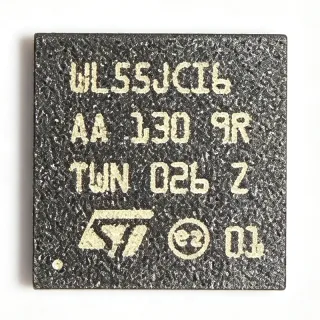
MS22300 - 10G Dual-CDR Multi-Rate Optical Transceiver | Minisilicon
Référence : MS22300 ✗ Fin de vie| Qté | Prix unitaire | Total |
|---|---|---|
| 1 | $0 | $0,00 |
| 10 | $0 | $0,00 |
| 100 | $0 | $0,00 |
| 500 | $0 | $0,00 |
| 1 000 | $0 | $0,00 |
MS22300 Présentation
A clock and data recovery (CDR) circuit is a high-speed signal-conditioning component that extracts timing information from a serial data stream and regenerates a clean, phase-aligned output. In an optical transceiver, the CDR works with the laser driver and receive-side limiting amplifier to support reliable data transfer over optical media. The MS22300’s combination of these functions can reduce the external signal-chain component count in a retiming-module design, while its digital control interfaces provide a path for configuration and optimization.
The MS22300 product information highlights an improved APC loop with extended dynamic range and high resolution. APC means automatic power control, a feedback mechanism used to regulate optical output power and compensate for component and environmental variation. The verified manufacturer page describes MS22300 as an EML driver, limiting amplifier, and CDR solution intended to support multiple optical emission components. However, complete electrical timing, supply-voltage, power-consumption, temperature, and pin-level specifications are not present in the supplied data, so those values remain marked for engineering verification.
The chip is positioned for 10G ER/ZR transceiver implementations. ER and ZR optical reaches are used in optical-networking systems where transmission distance and link-budget requirements differ. Because the supplied evidence specifically mentions 10G ER/ZR support, SFP+ retiming modules, SONET applications, and MS56-series TIA pairing, those are the primary design contexts supported by this record. The QFN32 4x4 package can also support compact module layouts, but the exposed-pad and thermal details must be confirmed from the official MS22300 datasheet before PCB release.
This page combines the verified manufacturer descriptions with transparent data gaps rather than inventing unprovided electrical specifications. Engineers should confirm supply rails, high-speed differential I/O requirements, pin mapping, protocol coverage, optical-launch behavior, receive sensitivity, thermal limits, and control-register compatibility with the manufacturer datasheet and application support. For a production design, the MS22300 should be treated as a specialized optical-transceiver IC, not as a generic digital logic or memory component.
Alternatives de remplacement direct pour MS22300 — même boîtier, compatible broche à broche. Les références à boîtier différent nécessitant une retouche du PCB sont exclues.
Outil de comparaison rapide — sélectionnez des références alternatives pour une comparaison côte à côte :
Aucune alternative de remplacement direct disponible pour ce produit.
Demander des alternativesMS22300 Spécifications
| Product Type | Integrated bidirectional 10G CDR, EML laser driver, and limiting amplifier transceiver |
| Débit de données | 10 Gbps |
| Clock and Data Recovery | Integrated dual-CDR |
| Laser Driver Type | EML laser driver |
| Receive Amplifier | Integrated limiting amplifier |
| Automatic Power Control | On-chip APC function with extended dynamic range and high resolution |
| Control Interface | Standard IIC interface |
| Digital Control | On-chip digital control circuit |
| Optical Reach Application | 10G ER/ZR transceiver |
| Module Application | Low-power SFP+ retiming module |
| Standards Context | SONET |
| Compatible TIA Family | MS56-series 10G TIA |
| Boîtier | QFN32 4x4 |
| Nombre de broches | 32 pins |
| Statut RoHS | Not verified for MS22300; only the JLCPCB result uses the term ROHS |
Guide de configuration des broches du MS22300 qfn32 4x4
Configuration des broches du MS22300 (boîtier qfn32 4x4). La numérotation des broches, les fonctions et les schémas de connexion sont définis dans la fiche technique du fabricant. Consultez-la pour l'empreinte exacte et les directives de soudage.
Aucune donnée de brochage détaillée disponible pour MS22300.
Consultez la fiche technique pour la configuration complète des broches.
Applications typiques
MS22300 convient pour 6 applications: 10G ER/ZR Optical Transceivers, Low-Power SFP+ Retiming Modules, SONET High-Speed Optical Links, Bidirectional Optical Data Links, 10G Optical Module Clock Recovery, Optical Communication Test and Measurement.
10G ER/ZR Optical Transceivers
The MS22300 fits 10G ER/ZR transceiver designs because the verified Minisilicon information identifies it as part of a 10Gbps ER/ZR chipset and combines an EML laser driver, dual-CDR, and limiting amplifier. Placing these functions in one QFN32 4x4 device can simplify the transmit and receive signal chain compared with a separated implementation. The design must still validate optical launch power, extinction ratio, receive sensitivity, wavelength, link budget, thermal rise, and reach against the specific ER or ZR channel. The MS56-series TIA is identified by the verified sources as a possible companion for the receive path.
Recommandé
Low-Power SFP+ Retiming Modules
The MS22300 is explicitly described by Minisilicon as a solution for low-power SFP+ retiming modules. Its integrated dual-CDR, EML driver, limiting amplifier, APC function, IIC interface, and digital control can reduce the number of discrete high-speed blocks around the optical engine. That consolidation is useful when module space, power, and component count are constrained. Engineering validation should focus on the module’s supported data rates, electrical lane requirements, thermal environment, startup behavior, and whether the host expects standard SFP+ control semantics. The supplied data does not specify module power or board-level thermal limits.
Recommandé
SONET High-Speed Optical Links
The verified Minisilicon product description specifically references SONET in connection with the MS22300’s use in low-power SFP+ timing modules. Its CDR function is intended to recover timing from high-speed serial data, while the EML driver and limiting amplifier support transmit and receive conditioning. SONET deployment decisions must be based on the exact rate, wavelength, optical reach, jitter, BER, and protocol-support tables from the manufacturer datasheet. The available data does not identify a SONET rate or jitter mask, so those values must not be inferred from the general 10Gbps description.
Recommandé
Bidirectional Optical Data Links
The MS22300 is identified as an integrated bidirectional transceiver with CDR, EML laser-driver, and limiting-amplifier functions. This architecture is relevant to optical links that require both transmit and receive conditioning close to the module boundary, particularly in compact pluggable or retiming designs. The designer should verify whether the device handles both directions internally, what external optics and filtering are required, and how the IIC control plane configures each path. Because the supplied data omits the complete pinout and electrical tables, interface partitioning must be confirmed before layout.
Recommandé
10G Optical Module Clock Recovery
The integrated dual-CDR makes the MS22300 relevant where a 10G optical module needs local timing recovery before data reaches a digital or packet-processing stage. Recovering timing close to the high-speed optical interface can reduce sensitivity to accumulated signal-integrity degradation, provided the CDR’s jitter tolerance, loop bandwidth, and equalization behavior are suitable. The verified data confirms CDR integration and SONET positioning but does not provide jitter specifications, latency, lock time, or reference-clock requirements. Those values must be obtained from the official documentation and tested across temperature and supply corners.
Recommandé
Optical Communication Test and Measurement
The MS22300’s combination of EML drive, limiting amplification, APC, and CDR can support test fixtures and characterization boards for 10G optical transmit/receive chains. Such a fixture can exercise the same integrated signal blocks used in an ER/ZR transceiver, simplifying correlation between optical performance and digital recovery behavior. The test fixture still needs accurate optical power measurement, thermal control, suitable test equipment, and a defined IIC control sequence. The verified data does not provide guaranteed performance limits or calibration procedures, so this use should be treated as a characterization context rather than a validated production test specification.
Recommandé
Récapitulatif des produits recommandés
Données de référence d'ingénierie pour MS22300 — comparaison, recommandations de conception et informations de conformité.
Guide de sélection
Comparaison avec les alternatives
| Paramètre | Ce produit | MS58050 |
|---|---|---|
| Brand | Minisilicon | Minisilicon |
| Data Rate | 10 Gbps | 10 Gbps |
| CDR Integration | Integrated dual-CDR | Not integrated according to verified description |
| EML Laser Driver | Integrated | Integrated |
| Limiting Amplifier | Integrated | Integrated |
| APC Function | On-chip APC with extended dynamic range and high resolution | On-chip APC |
| Control Interface | Standard IIC | Standard IIC |
| Target Optical Reach | 10G ER/ZR | 10G ER/ZR chipset context |
Principaux différenciateurs
- CDR integration beyond the related chipset description (vs MS58050)
- Single-chip functional consolidation (vs MS58050)
- Optical control architecture (vs MS58050)
Notes de conception
Treat the MS22300 as a high-speed mixed-signal RF/optical IC rather than a general-purpose digital device. Before routing, obtain the official pinout and differential-I/O electrical tables, then verify trace impedance, connector or optical-module transition geometry, return-path continuity, and reference-plane placement. The QFN32 4x4 package requires short, controlled connections around the high-speed pins; do not infer pin functions from the family description alone.
Use the manufacturer’s QFN32 land pattern and exposed-pad requirements when available. The supplied data confirms only the QFN32 4x4 package, not pad dimensions, pin numbering, thermal-pad geometry, or reflow profile. Confirm those details before releasing artwork, and provide uninterrupted ground and power distribution around the device. Keep the IIC control trace away from sensitive high-speed paths where practical, and validate the complete stack-up with controlled-impedance calculations.
Power sequencing and decoupling must be based on the MS22300’s official supply-voltage table, which is not included in the verified data. Do not select capacitor values, rail limits, or startup delays from generic optical-transceiver practice alone. Use the manufacturer’s recommended power architecture, validate voltage tolerances and ripple at the IC pins, and measure startup and shutdown behavior across temperature. The integrated CDR, EML driver, limiting amplifier, APC, and digital control may create transient loads that the system supply must handle.
Do not confuse MS22300 with the similarly named MS2230005-B inrush-current-limiter listings or with unrelated thermistor records returned by broad part-number searches. The verified MS22300 sources identify a Minisilicon optical transceiver chipset, not a passive circuit-protection device. Also avoid assuming that MS58050 is pin-compatible with MS22300: the descriptions state related functionality, but no verified pin-to-pin equivalence or drop-in footprint data is provided.
Informations de conformité
The supplied JLCPCB snippet contains the term ROHS, but it does not provide a compliance declaration for MS22300. RoHS, REACH, lead-free, halogen-free, and conflict-minerals status therefore remain unknown.