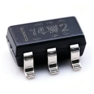
OPA170AIDBVT - 36V, 1.2MHz, Low-Power Op Amp | Texas Instruments
Référence : OPA170AIDBVT ✓ Actif| Qté | Prix unitaire | Total |
|---|---|---|
| 1 | $1.65 | $1,65 |
| 10 | $1.42 | $14,20 |
| 100 | $1.05 | $105,00 |
| 500 | $0.85 | $425,00 |
| 1 000 | $0.69 | $690,00 |
| 3 000 | $0.55 | $1 650,00 |
OPA170AIDBVT Présentation
What is a low-power operational amplifier? A low-power op amp is a class of analog amplifier IC designed to operate on single or dual supplies while consuming minimal quiescent current, enabling battery-powered and energy-efficient designs. Low-power op amps sit within the broader operational amplifier family, which belongs to linear ICs and the signal-conditioning product hierarchy. They balance bandwidth, offset, and noise against supply current, making them ideal for always-on sensor interfaces and portable instrumentation.
Key features include rail-to-rail output (RRO), an enable/shutdown pin for power sequencing, low offset voltage, low drift over temperature, and 1.2 MHz gain-bandwidth product. The device also provides ESD protection on the inputs/outputs and is specified over the -40 °C to +125 °C industrial temperature range. The 5-pin SOT-23 footprint enables extremely compact PCB designs for space-constrained analog front ends.
Architecturally, the OPA170 uses a bipolar input stage with CMOS output stages for rail-to-rail swing, and the family (OPA170/OPA2170/OPA4170) shares identical specifications across single, dual, and quad versions for easy design portability. The combination of 36 V tolerance, low quiescent current, and small packaging positions the OPA170 as a strong fit for industrial sensors, transducer signal conditioning, and active filtering.
Typical applications include current sensing in power management, transducer amplifiers for pressure/flow sensors, active filters, test equipment input buffers, and general-purpose signal conditioning for industrial control and battery-powered systems. Designers choose the OPA170 family when they need robust 36 V tolerance, low power, and rail-to-rail output in a tiny footprint.
When designing with this device, place a 0.1 µF decoupling capacitor as close as possible to the power-supply pin and ensure input common-mode range is respected. The shutdown/enable pin allows direct power-rail control in low-power duty-cycled applications.
This page synthesizes verified distributor pricing, parametric drop-in alternatives, and practical design guidance not found in the manufacturer datasheet, all anchored to the official TI OPA170 datasheet as of 2026-10-09.
Alternatives de remplacement direct pour OPA170AIDBVT — même boîtier, compatible broche à broche. Les références à boîtier différent nécessitant une retouche du PCB sont exclues.
Outil de comparaison rapide — sélectionnez des références alternatives pour une comparaison côte à côte :
OPA171AIDBVT
✅ Remplacement direct📋 Alternative de référence (hors catalogue)
OPA170AIDBVR
✅ Remplacement direct📋 Alternative de référence (hors catalogue)
OPA170AIDBVTG4
✅ Remplacement direct📋 Alternative de référence (hors catalogue)
OPA2170AIDBVR
✅ Remplacement direct📋 Alternative de référence (hors catalogue)
NCV20071SN3T1G
✅ Remplacement direct📋 Alternative de référence (hors catalogue)
TSZ1247IYPT
✅ Remplacement direct📋 Alternative de référence (hors catalogue)
MCP6001T-E/OT
✅ Remplacement direct📋 Alternative de référence (hors catalogue)
OPA170AIDBVT Valeurs maximales et caractéristiques électriques
| Manufacturer | Texas Instruments |
| Series | OPA170 |
| Amplifier Type | General Purpose Operational Amplifier |
| Number of Channels | 1 |
| Type de sortie | Rail-to-Rail |
| Supply Voltage Range (Single) | 2.7 V to 36 V |
| Supply Voltage Range (Dual) | ±1.35 V to ±18 V |
| Gain-Bandwidth Product (GBP) | 1.2 MHz |
| Slew Rate | 0.4 V/µs (typical) |
| Input Offset Voltage (Vos) | 1.5 mV (max) |
| Input Bias Current | 10 pA (typical) |
| Quiescent Current (per channel) | 110 µA (typical) |
| Plage de température de fonctionnement | -40 °C to +125 °C |
| Boîtier / Format | SOT-23-5 (DBV) |
| Type de montage | Surface Mount |
| Niveau MSL | 1 (Unlimited) |
| Statut RoHS | Compliant |
| Shutdown / Enable Pin | Yes |
Configuration des broches de OPA170AIDBVT
| Broche 1 | OUT — Amplifier output (rail-to-rail) |
| Broche 2 | V- — Negative supply (ground for single-supply) |
| Broche 3 | IN+ — Non-inverting input |
| Broche 4 | IN- — Inverting input |
| Broche 5 | EN/SHDN — Enable / shutdown (active-high) |
Applications typiques
OPA170AIDBVT convient pour 7 applications: Industrial 4-20 mA Current-Loop Signal Conditioning, Portable Sensor Signal Conditioning, Active Filters and Audio Signal Buffers, Automotive Sensor and Body Electronics, Test and Measurement Input Buffers, Power-Supply Current Sensing, General-Purpose Comparator / Threshold Detector.
Industrial 4-20 mA Current-Loop Signal Conditioning
The OPA170AIDBVT's 36 V supply tolerance and ~110 µA quiescent current make it an excellent fit for 4-20 mA current-loop transmitter analog front ends. With 1.2 MHz GBP and 1.5 mV max offset, the part provides accurate amplification of sensor-derived currents while tolerating the loop compliance voltage (typically 24 V). Compared to 5 V op amps, the OPA170 eliminates the need for additional voltage-clamping circuitry on the loop supply rail. Used in pairs: one channel senses shunt voltage for current regulation, the second (in OPA2170) handles HART modem coupling or loop diagnostics. Designers value the shutdown pin for loop-power duty cycling in battery or solar-powered remote transmitters.
Recommandé
Portable Sensor Signal Conditioning
The OPA170AIDBVT's 1.2 MHz GBP at only 110 µA quiescent current gives it an excellent bandwidth-to-power ratio for portable sensor front ends (pressure, flow, temperature). Rail-to-rail output swing maximizes dynamic range on low-voltage single-cell Li-ion rails (3.0-4.2 V). The enable/shutdown pin lets the host MCU power-gate the op amp between measurements, extending battery life. Compared to zero-drift alternatives like the OPA378, the OPA170 offers higher supply tolerance for use directly from a 12 V battery stack or USB-boosted rail. It is commonly used in IoT sensor hubs, handheld medical instruments, and wireless condition-monitoring nodes.
Recommandé
Active Filters and Audio Signal Buffers
The OPA170AIDBVT's 1.2 MHz GBP is sufficient to build Sallen-Key or multiple-feedback active filters with cutoff frequencies up to ~100 kHz, ideal for anti-aliasing ahead of an audio-bandwidth ADC or for post-DAC reconstruction. Its rail-to-rail output allows clean ±5 V swing from a single 12 V supply, replacing legacy dual-supply op amps in cost-sensitive audio paths. The 0.4 V/µs slew rate avoids distortion on transient audio edges up to 20 kHz. In portable audio designs it pairs well with the TLV320AIC3254 codec or PCM5102A DAC; in industrial designs it serves as a transducer pre-filter.
Recommandé
Automotive Sensor and Body Electronics
The OPA170 family (qualified via the OPA170-Q1 automotive variant) handles automotive sensor signal conditioning for body-electronics modules and battery-management systems. With 36 V load-dump tolerance and rail-to-rail output, the op amp can be powered directly from the 12 V automotive bus without external protection in many cases. The low 110 µA Iq minimizes quiescent drain on always-on modules such as key fob receivers and intrusion detectors. Compared to legacy LM2902/LM358 designs, the OPA170 offers ~10x lower offset and bandwidth headroom for motor-current sensing via low-side shunts.
Recommandé
Test and Measurement Input Buffers
The OPA170AIDBVT's 36 V supply range and low offset make it a useful input buffer for low-frequency test instruments such as handheld multimeters, oscilloscope front ends, and data-acquisition modules. Its ability to accept ±18 V inputs without damage means it can directly interface to high-voltage dividers without external clamps. The SOT-23-5 footprint allows dense channel multiplexing in multi-channel DAQ boards. When paired with a precision reference such as the REF3125 and a 16-24 bit ADC like the ADS1256, the OPA170 enables 16-bit-class measurement accuracy in cost-sensitive industrial instruments.
Recommandé
Power-Supply Current Sensing
Low-side and high-side current-sense amplifiers built around the OPA170AIDBVT leverage its 36 V supply tolerance and rail-to-rail output to monitor power-supply load currents in industrial and telecom systems. A simple difference-amplifier configuration with the OPA170 gives a low-cost alternative to dedicated current-sense amplifiers. The 1.2 MHz GBP supports closed-loop bandwidths up to ~100 kHz, sufficient for switching-converter current-mode control loops. Compared to the INA180 family, this discrete approach is cheaper in single-channel designs but requires external precision resistors for gain accuracy.
Recommandé
General-Purpose Comparator / Threshold Detector
Although primarily an op amp, the OPA170AIDBVT can be configured as a low-power threshold detector or window comparator for battery-monitoring and over-voltage protection circuits. Its shutdown pin enables <1 µA quiescent state when the monitored rail is within limits, then wakes the system on a fault event. With 1.2 MHz GBP and 0.4 V/µs slew rate, it can respond to transients in the audio-to-ultrasonic band, suitable for ultrasonic sensing or motor stall detection. This application takes advantage of the OPA170's wide supply tolerance and small footprint for compact protection or alarm circuits.
Recommandé
Récapitulatif des produits recommandés
Données de référence d'ingénierie pour OPA170AIDBVT — comparaison, recommandations de conception et informations de conformité.
Guide de sélection
Comparaison avec les alternatives
| Paramètre | Ce produit | OPA171AIDBVT | OPA170AIDBVR | OPA2170AIDBVR | NCV20071SN3T1G | TSZ1247IYPT |
|---|---|---|---|---|---|---|
| Brand | Texas Instruments | Texas Instruments | Texas Instruments | Texas Instruments | onsemi | STMicroelectronics |
| Package | SOT-23-5 (DBV) | SOT-23-5 (DBV) - same | SOT-23-5 (DBV) - same | SOT-23-5 (DBV) - same | SOT-23-5 - same | SOT-23-5 - same |
| Supply Voltage (max) | 36 V | 36 V | 36 V | 36 V | 36 V | 18 V |
| Gain-Bandwidth Product | 1.2 MHz | 1.2 MHz | 1.2 MHz | 1.2 MHz | 0.9 MHz | 0.4 MHz |
| Quiescent Current (typ) | 110 µA | 110 µA | 110 µA | 110 µA/ch | 120 µA | 800 µA |
| Input Offset Voltage (max) | 1.5 mV | 1.5 mV | 1.5 mV | 1.5 mV | 3.0 mV | 25 µV (chopper) |
| Output Type | Rail-to-Rail Out | Rail-to-Rail Out | Rail-to-Rail Out | Rail-to-Rail Out | Rail-to-Rail I/O | Rail-to-Rail Out |
| Shutdown Pin | Yes | Yes | Yes | Yes | Yes | No |
| Automotive Grade | No (Q1 variant is) | No | No | No | Yes (AEC-Q100) | Yes (AEC-Q100) |
Principaux différenciateurs
- Wide 36 V supply tolerance in a SOT-23-5 package (vs MCP6001T-E/OT)
- Lower offset than generic 36 V op amps (vs LM358-family)
- Enable pin for power gating vs legacy op amps (vs OPA171AIDBVT (same family, no shutdown advantage))
Notes de conception
Estimated power dissipation: at 36 V single supply with 5 V output swing and 1 kohm load, the OPA170 dissipates ~31 mW; the SOT-23-5 thermal resistance (theta_JA) of ~200 °C/W yields a junction rise of ~6 °C above ambient, well within the 125 °C limit. For high-voltage single-supply designs where the op amp is permanently powered, ensure the input common-mode voltage stays within V- to (V+ - 1.5 V). Place a 0.1 µF X7R ceramic bypass capacitor within 5 mm of the V+ pin to prevent supply-induced oscillations.
Keep input traces short and shielded by a ground pour to minimize leakage and stray capacitance on the high-impedance inputs. For Sallen-Key or multiple-feedback active filters, place the resistor and capacitor networks symmetrically around the inverting/non-inverting pins and route the output trace away from IN+ to prevent feedback oscillation. The exposed thermal pad is not present on SOT-23-5, so copper pours on the V- pin help dissipate heat only marginally; for >50 mW dissipation, consider the SOIC-8 OPA170AID variant instead.
Do not assume the input is rail-to-rail - the OPA170 input common-mode range is V- to (V+ - 1.5 V), so signals approaching V+ can cause input stage saturation and distortion. The enable pin is internally pulled down; tie it to V+ if shutdown is not used. The 1.2 MHz GBP is at unity gain - at higher closed-loop gains the bandwidth scales inversely, so an inverting x10 amplifier has only ~120 kHz usable bandwidth. The shutdown pin is not fail-safe; floating the enable pin can leave the part in indeterminate state during power-up.
Informations de conformité
RoHS and REACH compliant per TI product page; standard industrial grade - not AEC-Q100 qualified (choose OPA170-Q1 variants for automotive). Halogen-free and Pb-free terminal finish on G4 suffix parts.