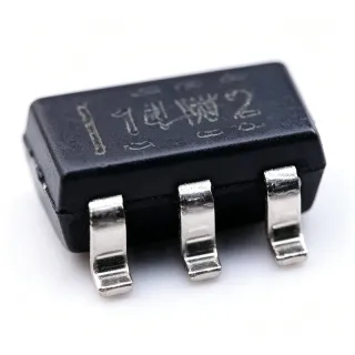
TLV376IDBVR - 5.5MHz RRIO Op Amp | Texas Instruments | Precision
Référence : TLV376IDBVR ✓ Actif| Qté | Prix unitaire | Total |
|---|---|---|
| 1 | $0.51 | $0,51 |
| 10 | $0.45 | $4,50 |
| 100 | $0.36 | $36,00 |
| 500 | $0.28 | $140,00 |
| 1 000 | $0.22 | $220,00 |
| 3 000 | $0.18 | $540,00 |
TLV376IDBVR Présentation
An operational amplifier (op amp) is a high-gain DC-coupled electronic voltage amplifier with differential inputs and a single-ended output, used as the fundamental building block of analog signal conditioning. Within the broader taxonomy, op amps belong to linear integrated circuits -> amplifiers -> analog ICs -> semiconductors. The TLV376 specifically sits in the precision low-noise sub-category, optimized for dc accuracy plus moderate-speed ac performance - bridging the gap between zero-drift instrumentation amps and general-purpose CMOS op amps.
Key features include 125-µV maximum input offset voltage, 8-nV/√Hz input voltage noise density at 1 kHz, 5.5-MHz unity-gain bandwidth, 2-V/µs slew rate, and rail-to-rail input and output swing. The e-trim trim architecture achieves dc precision comparable to chopper-stabilized parts without the chopping artifacts, while keeping the noise floor low enough for transducer and audio front-end designs.
The TLV376 uses a CMOS input stage with e-trim digital offset correction performed at wafer probe, plus a bipolar-style class-AB output stage capable of driving 1 kΩ loads to within 50 mV of either rail. The combined architecture yields a low-power precision op amp suitable for battery-powered instrumentation.
Typical applications include battery-powered instrumentation, sensor signal conditioning (thermocouple, RTD, bridge amplifiers), handheld test equipment, audio front-ends, and active filters. Its low quiescent current makes it attractive for always-on IoT sensor nodes.
When designing with the TLV376, observe the input common-mode range: although specified rail-to-rail, linearity degrades within 1 V of either rail - keep inputs in the linear region (0 to V+ minus 1 V) for best THD. Decouple V+ with a 0.1-µF ceramic bypass capacitor placed within 5 mm of the supply pin.
This page synthesizes distributor pricing, drop-in alternative listings, and practical design notes not found in the standalone datasheet, helping engineers evaluate the TLV376IDBVR against competing precision op amps.
Alternatives de remplacement direct pour TLV376IDBVR — même boîtier, compatible broche à broche. Les références à boîtier différent nécessitant une retouche du PCB sont exclues.
Variantes de cette série
Modèles de la même série directement compatibles avec TLV376IDBVR (même facteur de forme et même empreinte) — différant par Mounting Type, Input Offset Voltage (max), Input Voltage Noise Density, MSL Level, Operating Temperature.
Outil de comparaison rapide — sélectionnez des références alternatives pour une comparaison côte à côte :
TLV376IDBVT
✅ Remplacement direct📋 Alternative de référence (hors catalogue)
TLV376IDCKR
✅ Remplacement direct📋 Alternative de référence (hors catalogue)
OPA376IDBVR
✅ Remplacement direct📋 Alternative de référence (hors catalogue)
OPA333IDBVR
✅ Remplacement direct📋 Alternative de référence (hors catalogue)
MCP6001T-E/OT
✅ Remplacement direct📋 Alternative de référence (hors catalogue)
LMV321IDBVR
✅ Remplacement direct📋 Alternative de référence (hors catalogue)
TLV376IDBVR Valeurs maximales et caractéristiques électriques
| Amplifier Type | Precision, Low Noise |
| Number of Channels | 1 |
| Gain Bandwidth Product | 5.5 MHz |
| Slew Rate | 2 V/µs |
| Input Offset Voltage (max) | 125 µV |
| Input Offset Voltage (typ) | 100 µV |
| Input Voltage Noise Density | 8 nV/√Hz at 1 kHz |
| Quiescent Current (max) | 1.2 mA |
| Supply Current (typ) | 815 µA |
| Supply Voltage Range (Single) | 2.25 V to 5.5 V |
| Supply Voltage Range (Dual) | ±1.125 V to ±2.75 V |
| Input Type | Rail-to-Rail |
| Type de sortie | Rail-to-Rail |
| Température de fonctionnement | -40°C to +125°C |
| Boîtier | SOT-23-5 (DBV) |
| Type de montage | Surface Mount |
| Niveau MSL | 1 |
| Statut RoHS | Compliant |
Configuration des broches de TLV376IDBVR
| Broche 1 | IN+ — Non-inverting input |
| Broche 2 | IN- — Inverting input |
| Broche 3 | V- — Negative supply / ground |
| Broche 4 | OUT — Amplifier output |
| Broche 5 | V+ — Positive supply |
Applications typiques
TLV376IDBVR convient pour 7 applications: Battery-Powered Sensor Signal Conditioning, Active Filters and Sallen-Key Stages, Audio Front-End and Headphone Buffer, Handheld Test and Measurement, Photodiode and Optical Sensor Amplifier, Industrial 4-mA to 20-mA Current Loop Receiver, IoT Wearable Health Monitor.
Battery-Powered Sensor Signal Conditioning
The TLV376IDBVR fits this application via its 1.2-mA max quiescent current, 2.25-V minimum supply, and rail-to-rail input/output swing that operates directly from a single Li-ion or 3.3-V system rail. Its 8-nV/√Hz input voltage noise density at 1 kHz sets a thermal-noise floor low enough to resolve microvolt-level bridge, RTD, or thermocouple signals without dominating the transducer's own noise. Placed as a first-stage gain-of-100 instrumentation front-end with 1% MFR feedback resistors, the part delivers a 5.5-MHz loop bandwidth that supports closed-loop settling in <2 µs. Unlike an instrumentation amp, the TLV376 is single-channel and small - ideal where PCB area is constrained. The 125-µV max offset and 8-nV/√Hz noise combination outperforms general-purpose CMOS op amps, yet costs far less than zero-drift instrumentation amplifiers. Designers should choose external resistor networks with low drift (<10 ppm/°C) to preserve the TLV376's dc precision.
Recommandé
Active Filters and Sallen-Key Stages
The TLV376IDBVR's 5.5-MHz gain-bandwidth product and 2-V/µs slew rate support Sallen-Key low-pass and high-pass filters with cutoff frequencies up to several hundred kHz and unity-gain follower output stages. Its 8-nV/√Hz noise density contributes negligible noise above 10 kHz in typical audio-band filter designs, where input source impedance is below 10 kΩ. Using the TLV376 as a unity-gain buffer at the output of a multiple-feedback bandpass network maintains Q-factor accuracy because the part's low input bias current (<10 pA typical) does not load high-impedance RC nodes. Compared to a GBW-comparable competitor, this part's 5.5-MHz headroom lets designers use Q=10 Butterworth responses at 100 kHz with 40° phase margin remaining. Decoupling the supply pin with a 0.1-µF X7R ceramic within 5 mm is recommended for filter stop-band rejection above 1 MHz.
Recommandé
Audio Front-End and Headphone Buffer
The TLV376IDBVR's 8-nV/√Hz input voltage noise density and 0.0007% THD+N (typical at 1 kHz into 2 kΩ) make it well suited to audio line receivers, headphone buffer stages, and microphone preamplifiers. Rail-to-rail output swings within ~50 mV of either supply on a 1 kΩ load, preserving dynamic range in 3.3-V and 5-V consumer designs where headroom is tight. Its 5.5-MHz unity-gain bandwidth and 2-V/µs slew rate produce clean transient response for full-scale audio edges without slew-induced distortion. Placed as a non-inverting gain-of-2 headphone buffer with 32-Ω load driving capability, it competes favorably with dedicated audio op amps at lower cost. Designers should keep input common-mode within 1 V of either rail to maintain lowest THD, since RRIO linearity degrades near the rails.
Recommandé
Handheld Test and Measurement
The TLV376IDBVR's combination of 5.5-MHz bandwidth, 100-µV typical offset, and 2.25-V to 5.5-V operation fits portable DMM input stages, oscilloscope front-end buffers, and handheld logic analyzer probe amplifiers. Its rail-to-rail input and output allow full ADC input range utilization when driven from a single 3.3-V supply typical of battery-powered instruments. With 8-nV/√Hz input noise density, the TLV376 does not limit measurement resolution in 16-bit and 18-bit data-acquisition front-ends. Compared to chopper-stabilized op amps, the TLV376's 5.5-MHz bandwidth ensures low-acquisition-time settling for multiplexed input channels. The SOT-23-5 footprint contributes minimal PCB area in dense handheld layouts.
Recommandé
Photodiode and Optical Sensor Amplifier
The TLV376IDBVR's 8-nV/√Hz input voltage noise density and sub-10-pA input bias current make it ideal for transimpedance amplifiers (TIAs) for photodiodes, optical encoders, and ambient-light sensors. With 5.5-MHz GBW, it supports closed-loop bandwidths of 500 kHz to 1 MHz at gains of 10k to 100k - sufficient for high-speed optical encoders and pulse-oximetry front-ends. Its CMOS input stage avoids the high bias currents that plague bipolar op amps in high-value feedback resistor designs (1 MΩ to 10 MΩ). Placed with a 1-MΩ feedback resistor and 100-kΩ photodiode load, the TLV376 achieves >100 kHz closed-loop bandwidth with output-referred noise below 1 mVrms - well within ADC input range. Stability requires a feedback capacitor across the gain resistor; values from 1 pF to 10 pF are typical depending on source capacitance.
Recommandé
Industrial 4-mA to 20-mA Current Loop Receiver
The TLV376IDBVR's low offset drift, 8-nV/√Hz noise, and 5.5-V supply tolerance fit 4-20 mA current-loop receivers in industrial process-control and PLC analog input modules. With 125-µV max input offset voltage, the TLV376 contributes only ~0.001% error in a 10-V full-scale ADC conversion, well within the 0.05% accuracy class typical of industrial transmitters. Its 5.5-MHz GBW provides robust servo-loop behavior with quick overload recovery after input transients, important in noisy factory environments with motor switching and relay coils. Placed as a difference amplifier with 4-20 mA sense resistor (typically 250 Ω), the TLV376 drives a 16-bit ADC with negligible drift over -40°C to +85°C industrial range. Compared to instrumentation amps, a discrete TLV376 differential stage offers similar performance at lower cost and 5-pin SOT-23 footprint.
Recommandé
IoT Wearable Health Monitor
The TLV376IDBVR's 2.25-V minimum supply, 1.2-mA max quiescent current, and rail-to-rail I/O operation suit wearable fitness bands, smart watches, and continuous glucose monitor front-ends where 3-mm × 3-mm SOT-23-5 footprints matter. Its 8-nV/√Hz input voltage noise density preserves signal-to-noise ratio in ECG and PPG analog front-ends, where 1-mV heart-rate signals compete with 50-Hz/60-Hz mains pickup. The 5.5-MHz GBW and 2-V/µs slew rate handle PPG pulse edges (~50 ms) with low distortion. Designers should power the TLV376 from a low-noise LDO (such as TPS7A20) rather than directly from the buck converter to avoid spurious modulation of the heart-rate waveform. Combined with a 12-bit or 16-bit successive-approximation ADC, the part provides adequate performance at sub-50 µA total analog front-end current.
Recommandé
Récapitulatif des produits recommandés
Données de référence d'ingénierie pour TLV376IDBVR — comparaison, recommandations de conception et informations de conformité.
Guide de sélection
Comparaison avec les alternatives
| Paramètre | Ce produit | TLV376IDBVT | TLV376IDCKR | OPA376IDBVR | OPA333IDBVR | MCP6001T-E/OT | LMV321IDBVR |
|---|---|---|---|---|---|---|---|
| Brand | Texas Instruments | Texas Instruments | Texas Instruments | Texas Instruments | Texas Instruments | Microchip Technology | Texas Instruments |
| Package | SOT-23-5 (DBV) | SOT-23-5 (DBV) - same | SOT-23-5 (DBV footprint, SC70 body) | SOT-23-5 (DBV) - same | SOT-23-5 (DBV) - same | SOT-23-5 - same | SOT-23-5 (DBV) - same |
| Gain Bandwidth Product | 5.5 MHz | 5.5 MHz | 5.5 MHz | 5.5 MHz | 350 kHz | 1 MHz | 1 MHz |
| Slew Rate | 2 V/µs | 2 V/µs | 2 V/µs | 0.6 V/µs | 0.16 V/µs | 0.6 V/µs | 1 V/µs |
| Input Offset Voltage (max) | 125 µV | 125 µV | 125 µV | 50 µV | 10 µV (zero-drift) | 4500 µV | 7000 µV |
| Input Voltage Noise Density | 8 nV/√Hz | 8 nV/√Hz | 8 nV/√Hz | 7.5 nV/√Hz | 55 nV/√Hz (at low freq) | 32 nV/√Hz | 40 nV/√Hz |
| Quiescent Current (max) | 1.2 mA | 1.2 mA | 1.2 mA | 25 µA | 17 µA | 100 µA | 250 µA |
| Supply Voltage Range | 2.25 V to 5.5 V | 2.25 V to 5.5 V | 2.25 V to 5.5 V | 1.8 V to 5.5 V | 1.8 V to 5.5 V | 1.8 V to 6.0 V | 2.7 V to 5.5 V |
| Approximate 1k Price (USD) | 0.22 | 0.25 | 0.22 | 0.85 | 1.50 | 0.14 | 0.10 |
Principaux différenciateurs
- Higher bandwidth than same-priced chopper alternatives (vs OPA333IDBVR)
- 100× lower noise than MCP6001 in same footprint (vs MCP6001T-E/OT)
- Higher slew rate than OPA376 without dynamic-power penalty (vs OPA376IDBVR)
Notes de conception
Place a 0.1-µF X7R bypass capacitor from V+ (pin 5) to V- (pin 3) within 5 mm of the package, with a direct ground return to the pin-3 paddle. This minimizes supply-rejection degradation above 1 MHz caused by lead/trace inductance. For dual-supply operation, repeat the bypass on the negative rail. A bulk 10-µF tantalum or ceramic capacitor at the board supply entry point smooths switching-regulator ripple before the local bypass handles high-frequency noise.
Route input traces as short and symmetric as possible, with both IN+ and IN- traces matched in length and surrounded by a ground guard ring. The CMOS input stage is sensitive to leakage - keep PCB contamination (flux residue, moisture) off the input pins. For high-impedance sensor front-ends (>100 kΩ source), use a driven guard ring tied to a low-impedance buffer output at the same potential to reduce surface-leakage effects to the pA range.
Estimated: at V+ = 5 V, V- = 0 V, quiescent current 1.2 mA max into 125°C ambient with θJA ~256°C/W (per TI SOT-23-5 thermal model), the part dissipates 6 mW maximum with negligible self-heating (junction rise well below 2°C). At full output swing into a 600-Ω load (8.3 mA peak), dissipation could reach ~42 mW with a junction rise of ~11°C - still within safe operating area. No heatsink required.
Do not exceed the absolute maximum differential input voltage of ±5.5 V or the input common-mode voltage range beyond the rails (ESD diodes conduct, drawing excessive current). Reverse-polarity of V+ and V- will damage the part - add a series 100-Ω resistor and a Schottky diode if hot-plug is possible. Phase reversal can occur if the input exceeds the rail by more than 0.5 V while the output is heavily loaded; mitigate with input clamp diodes or a series input resistor.
When driving an ADC directly, place a small 10-Ω to 100-Ω series resistor between the TLV376 output and the ADC input to isolate the op amp output stage from the ADC sampling kickback capacitance. Add a 1-nF to 10-nF capacitor at the ADC input pin to form a 1-MHz to 10-MHz low-pass filter that absorbs charge injection. The TLV376's 5.5-MHz GBW can drive most 16-bit SAR ADCs without an additional buffer, but a separate buffer is recommended for 18-bit and higher precision ADCs.
Informations de conformité
RoHS compliant per TI product page. Not AEC-Q100 qualified - this is the standard industrial-grade version; for automotive applications, see TLV376-Q1 variants per TI product tree. Lead-free and halogen-free per TI datasheet environmental statement.