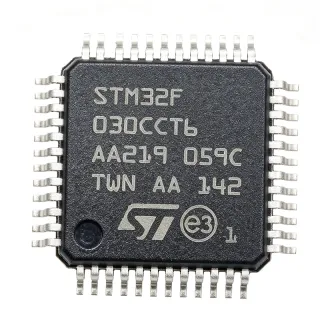
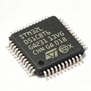
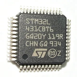
STM32C071C8T6 - 32-bit ARM Cortex-M0+ MCU, 64KB Flash | STMicroelectronics
Référence : STM32C071C8T6 ✓ Actif| Qté | Prix unitaire | Total |
|---|---|---|
| 1 | $2.15 | $2,15 |
| 10 | $1.93 | $19,30 |
| 100 | $1.72 | $172,00 |
| 500 | $1.55 | $775,00 |
| 1 000 | $1.38 | $1 380,00 |
STM32C071C8T6 Présentation
A microcontroller (MCU) is a compact integrated circuit that combines a processor core, memory, and programmable input/output peripherals on a single chip. The STM32C071C8T6 belongs to the STM32 family, which is a broad portfolio of 32-bit MCUs based on ARM Cortex-M cores. Within the STM32C0 series, it targets entry-level applications that require a balance of performance, low power, and affordability. The Cortex-M0+ core is an energy-efficient processor optimized for simple control tasks, making it suitable for IoT devices, consumer electronics, and industrial control.
Key features include a 12-bit ADC with up to 16 channels, multiple timers (including a 16-bit advanced-control timer), and a rich set of communication interfaces: I2C, SPI, USART, and a low-power UART. The device supports a wide supply voltage range of 2.0V to 3.6V, with an operating temperature range of -40°C to +85°C. It also includes a real-time clock (RTC), a CRC calculation unit, and a unique device ID for traceability.
The STM32C071C8T6 is built on a 90nm process technology, offering low dynamic power consumption. It features multiple low-power modes (Sleep, Stop, Standby) to optimize energy usage in battery-powered designs. The device includes a nested vectored interrupt controller (NVIC) for efficient interrupt handling, and a memory protection unit (MPU) for enhanced security. The LQFP-48 package provides a compact footprint while offering sufficient I/O pins for peripheral connectivity.
Typical applications include home automation sensors, smart appliances, portable medical devices, and industrial monitoring systems. Its low power consumption and rich peripheral set make it ideal for battery-operated IoT nodes that require periodic sensor readings and wireless communication. The device also supports firmware updates via a built-in bootloader, simplifying field maintenance.
When designing with this MCU, ensure proper decoupling of the VDD pins with 100nF capacitors placed close to the device. The VDDA pin should be connected to a clean analog supply to minimize ADC noise. For low-power operation, configure unused GPIOs as analog inputs to reduce leakage current.
Alternatives de remplacement direct pour STM32C071C8T6 — même boîtier, compatible broche à broche. Les références à boîtier différent nécessitant une retouche du PCB sont exclues.
Outil de comparaison rapide — sélectionnez des références alternatives pour une comparaison côte à côte :
STM32C071C6T6
✅ Remplacement direct📋 Alternative de référence (hors catalogue)
STM32C071C8T7
✅ Remplacement direct ⚠️ Spécifications non vérifiées📋 Alternative de référence (hors catalogue)
STM32G071C8T6
⚡ Même boîtier ⚠️ Spécifications non vérifiées✓ En stock
$2.8 / unité
Voir la fiche technique →STM32C071C8T6 Valeurs maximales et caractéristiques électriques
| Core | ARM Cortex-M0+ |
| Max Clock Speed | 48 MHz |
| Flash Memory | 64 KB |
| SRAM | 16 KB |
| Tension d'alimentation | 2.0 V to 3.6 V |
| Température de fonctionnement | -40C to +85C |
| Boîtier | LQFP-48 (7x7 mm) |
| ADC | 12-bit, up to 16 channels |
| Timers | Multiple 16-bit timers, 1 advanced-control |
| Communication Interfaces | I2C, SPI, USART, LPUART |
| GPIO Pins | Up to 38 |
| DMA | Yes, 7 channels |
| RTC | Yes |
| Low Power Modes | Sleep, Stop, Standby |
| Statut RoHS | Compliant |
Configuration des broches de STM32C071C8T6
| Broche 1 | VBAT — Battery backup supply for RTC |
| Broche 2 | PC14 — GPIO / OSC32_IN |
| Broche 3 | PC15 — GPIO / OSC32_OUT |
| Broche 4 | PF0 — GPIO / OSC_IN |
| Broche 5 | PF1 — GPIO / OSC_OUT |
| Broche 6 | NRST — Reset (active low) |
| Broche 7 | VDD — Digital power supply |
| Broche 8 | VSS — Ground |
| Broche 9 | PA0 — GPIO / ADC_IN0 |
| Broche 10 | PA1 — GPIO / ADC_IN1 |
| Broche 11 | PA2 — GPIO / USART2_TX |
| Broche 12 | PA3 — GPIO / USART2_RX |
| Broche 13 | PA4 — GPIO / SPI1_NSS |
| Broche 14 | PA5 — GPIO / SPI1_SCK |
| Broche 15 | PA6 — GPIO / SPI1_MISO |
| Broche 16 | PA7 — GPIO / SPI1_MOSI |
| Broche 17 | PB0 — GPIO / ADC_IN8 |
| Broche 18 | PB1 — GPIO / ADC_IN9 |
| Broche 19 | PB2 — GPIO / BOOT1 |
| Broche 20 | PB10 — GPIO / I2C2_SCL |
| Broche 21 | PB11 — GPIO / I2C2_SDA |
| Broche 22 | VSS — Ground |
| Broche 23 | VDD — Digital power supply |
| Broche 24 | PB12 — GPIO / SPI2_NSS |
| Broche 25 | PB13 — GPIO / SPI2_SCK |
| Broche 26 | PB14 — GPIO / SPI2_MISO |
| Broche 27 | PB15 — GPIO / SPI2_MOSI |
| Broche 28 | PA8 — GPIO / MCO |
| Broche 29 | PA9 — GPIO / USART1_TX |
| Broche 30 | PA10 — GPIO / USART1_RX |
| Broche 31 | PA11 — GPIO / USB_DM |
| Broche 32 | PA12 — GPIO / USB_DP |
| Broche 33 | PA13 — GPIO / SWDIO |
| Broche 34 | PA14 — GPIO / SWCLK |
| Broche 35 | PA15 — GPIO / JTDI |
| Broche 36 | PB3 — GPIO / JTDO |
| Broche 37 | PB4 — GPIO / NJTRST |
| Broche 38 | PB5 — GPIO / I2C1_SMBA |
| Broche 39 | PB6 — GPIO / I2C1_SCL |
| Broche 40 | PB7 — GPIO / I2C1_SDA |
| Broche 41 | BOOT0 — Boot mode selection |
| Broche 42 | PB8 — GPIO / CAN_RX |
| Broche 43 | PB9 — GPIO / CAN_TX |
| Broche 44 | VDD — Digital power supply |
| Broche 45 | VSS — Ground |
| Broche 46 | VDDA — Analog power supply |
| Broche 47 | PC13 — GPIO / RTC_TAMP1 |
| Broche 48 | PC14 — GPIO / OSC32_IN |
Applications typiques
STM32C071C8T6 convient pour 6 applications: Home Automation Sensors, Smart Appliances, Portable Medical Devices, Industrial Monitoring, IoT Edge Nodes, Consumer Electronics.
Home Automation Sensors
The STM32C071C8T6 is ideal for home automation sensors such as temperature, humidity, and motion detectors. Its low power consumption in Stop mode (typically 1.2 uA) allows battery-powered operation for years. The 12-bit ADC reads analog sensor outputs, while the I2C interface connects to digital sensors. The MCU can wake periodically, process data, and transmit via a sub-GHz radio or BLE module. Its 48 MHz Cortex-M0+ core provides sufficient processing for sensor fusion algorithms, and the 64 KB Flash stores calibration data and firmware. The wide supply voltage range (2.0V-3.6V) accommodates battery voltage drop over time. Designers can use the RTC to schedule wake-ups, and the LPUART for low-power communication with a host controller. The LQFP-48 package offers enough GPIOs for multiple sensor inputs and status LEDs.
Recommandé
Smart Appliances
In smart appliances like washing machines, refrigerators, and coffee makers, the STM32C071C8T6 provides control and connectivity. Its multiple timers generate PWM signals for motor control and heater regulation. The USART interface communicates with user interface panels or Wi-Fi modules. The 12-bit ADC monitors current and voltage for safety and efficiency. The MCU's 64 KB Flash stores complex state machines and user settings. The low-power modes allow the appliance to enter Standby when idle, reducing energy consumption. The device's robust operating temperature range (-40°C to +85°C) ensures reliability in kitchen environments. The LQFP-48 package fits on compact control boards, and the DMA controller offloads data transfer from peripherals, freeing the CPU for control loops. The RTC enables scheduled operations, such as delayed start in washing machines.
Recommandé
Portable Medical Devices
The STM32C071C8T6 is suitable for portable medical devices like glucose meters, pulse oximeters, and blood pressure monitors. Its low power consumption extends battery life, critical for handheld devices. The 12-bit ADC with up to 16 channels interfaces with biosensors, and the I2C/SPI ports connect to display drivers and memory. The Cortex-M0+ core efficiently runs signal processing algorithms for heart rate or glucose level calculation. The device's small LQFP-48 package enables compact PCB designs. The RTC tracks time for medication reminders, and the LPUART communicates with a smartphone via BLE. The MCU's wide supply voltage range (2.0V-3.6V) supports single-cell battery operation. The built-in CRC unit ensures data integrity for stored patient records. The operating temperature range covers clinical environments, and the device's reliability meets medical device standards.
Recommandé
Industrial Monitoring
For industrial monitoring systems, the STM32C071C8T6 offers reliable performance in harsh environments. Its -40°C to +85°C operating range suits factory floors and outdoor installations. The multiple timers and PWM outputs control actuators and alarms. The USART and SPI interfaces connect to industrial sensors, PLCs, and communication modules like RS-485 transceivers. The 12-bit ADC reads analog signals from pressure, temperature, and flow sensors. The MCU's DMA controller efficiently handles high-speed data acquisition. The 64 KB Flash stores configuration parameters and logging data. The device's low power consumption is beneficial for remote monitoring stations powered by solar or battery. The LQFP-48 package is easy to solder in automated assembly. The RTC provides timestamping for event logs, and the watchdog timer ensures system reliability in unattended operation.
Recommandé
IoT Edge Nodes
The STM32C071C8T6 is an excellent choice for IoT edge nodes that collect sensor data and transmit it to the cloud. Its low power consumption in Stop mode (1.2 uA) enables battery-powered operation for months. The MCU wakes periodically, reads sensors via I2C/SPI, processes data, and sends it via a wireless module (e.g., LoRa, BLE, or Wi-Fi). The 48 MHz Cortex-M0+ core handles protocol stacks like MQTT. The 64 KB Flash stores firmware and device certificates. The LPUART provides a low-power interface to the radio module. The device's wide supply voltage range (2.0V-3.6V) supports various battery chemistries. The RTC schedules wake-ups, and the DMA reduces CPU load during data transfer. The LQFP-48 package is compact for small sensor nodes. The MCU's security features, including a unique ID and CRC, support secure boot and data integrity.
Recommandé
Consumer Electronics
In consumer electronics like remote controls, smart plugs, and wearable devices, the STM32C071C8T6 provides cost-effective control. Its low power consumption extends battery life in remote controls. The 12-bit ADC reads battery voltage for low-battery indicators. The USART or I2C interfaces connect to IR transmitters or display drivers. The Cortex-M0+ core handles user input debouncing and protocol encoding. The 64 KB Flash stores button mappings and configuration. The device's small LQFP-48 package fits in slim enclosures. The RTC enables scheduled functions, such as smart plugs turning on at specific times. The MCU's wide supply voltage range (2.0V-3.6V) supports two AA batteries. The low-power modes allow the device to sleep between user interactions, consuming only microamps. The LQFP-48 package is cost-effective for high-volume production.
Recommandé
Récapitulatif des produits recommandés
Données de référence d'ingénierie pour STM32C071C8T6 — comparaison, recommandations de conception et informations de conformité.
Guide de sélection
Comparaison avec les alternatives
| Paramètre | Ce produit | STM32C071C6T6 | STM32C071C8T7 | STM32C071C8U6 | STM32G071C8T6 | LPC824M201JHI33 |
|---|---|---|---|---|---|---|
| Package | LQFP-48 | LQFP-48 (same) | LQFP-48 (same) | UFQFPN-48 (different) | LQFP-48 (same) | HVQFN-33 (different) |
| Brand | STMicroelectronics | STMicroelectronics | STMicroelectronics | STMicroelectronics | STMicroelectronics | NXP Semiconductors |
| Core | ARM Cortex-M0+ | ARM Cortex-M0+ | ARM Cortex-M0+ | ARM Cortex-M0+ | ARM Cortex-M0+ | ARM Cortex-M0+ |
| Max Clock Speed | 48 MHz | 48 MHz | 48 MHz | 48 MHz | 64 MHz | 30 MHz |
| Flash Memory | 64 KB | 32 KB | 64 KB | 64 KB | 64 KB | 32 KB |
| SRAM | 16 KB | 12 KB | 16 KB | 16 KB | 36 KB | 8 KB |
| Supply Voltage | 2.0V - 3.6V | 2.0V - 3.6V | 2.0V - 3.6V | 2.0V - 3.6V | 2.0V - 3.6V | 1.8V - 3.6V |
| ADC Resolution | 12-bit | 12-bit | 12-bit | 12-bit | 12-bit | 12-bit |
Principaux différenciateurs
- Higher Flash memory than base variant (vs STM32C071C6T6)
- Standard temperature range (vs STM32C071C8T7)
- LQFP-48 package with more GPIOs (vs STM32C071C8U6)
Notes de conception
Decouple each VDD pin with a 100nF ceramic capacitor placed as close as possible to the pin. Additionally, connect a 4.7uF capacitor to the main VDD rail. For VDDA, use a 1uF capacitor and a 10nF capacitor in parallel to filter high-frequency noise. Ensure the ground connections are low-impedance to minimize voltage drops.
For the LQFP-48 package, use a 0.5mm pitch land pattern. Provide a solid ground plane under the MCU to reduce EMI and improve thermal performance. Route the crystal oscillator (if used) with short traces and keep them away from high-speed digital lines. Add a series resistor (e.g., 33 ohms) on the SWD clock line to reduce ringing.
Do not leave unused GPIO pins floating; configure them as analog inputs or outputs to reduce leakage current. Ensure the BOOT0 pin is properly pulled low for normal boot mode. When using the ADC, connect VDDA to a clean analog supply and add a ferrite bead to isolate it from digital noise. Also, verify that the NRST pin has a 100nF capacitor to ground for reliable reset.
Informations de conformité
RoHS compliant per STMicroelectronics product page. Not AEC-Q100 qualified; for automotive, consider STM32C0 series with AEC-Q100 option.